

Page 1
Creating Embedded Systems
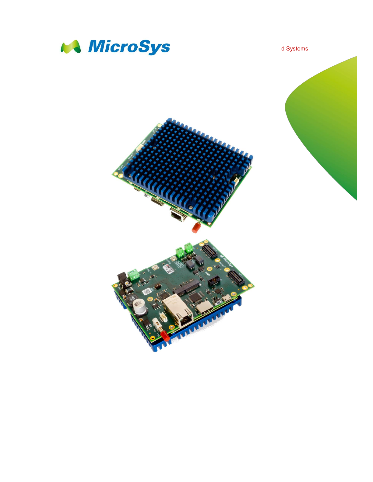
miriac SBC-S32V
User Manual
V 1.1
Page 2

Table of Contents
miriac SBC-S32V User Manual
V 1.1
2/81
© MicroSys Electronics GmbH 2017
Table of Contents
1 General Notes .............................................. 4
1.1 Warranty ........................................................ 4
1.2 Links .............................................................. 4
1.3 Liability .......................................................... 4
1.4 Offer to Provide Source Code of Certain
Software ........................................................ 5
1.5 Symbols, Conventions and Abbreviations ..... 6
1.5.1 Symbols ........................................................ 6
1.5.2 Conventions .................................................. 6
2 Introduction ................................................. 7
2.1 Safety and Handling Precautions .................. 7
2.2 Short Description ........................................... 8
2.3 Shipping List .................................................. 8
3 Quick Start Guide ........................................ 9
3.1 Prerequisites ................................................. 9
3.1.1 Minimum Requirements ................................ 9
3.1.2 Recommended Items .................................... 9
3.2 Board Preparation and Power-Up ............... 10
3.3 Operation .................................................... 12
3.3.1 U-Boot Startup............................................. 12
4 System Description ................................... 13
4.1 Block Diagram CRX-S32V Carrier ............... 13
4.2 Block Diagram MPX-S32V Module.............. 13
4.3 Feature Overview ........................................ 14
4.4 Mechanical Dimensions .............................. 17
4.4.1 MPX-S32V Module ...................................... 17
4.4.2 CRX-S32V Carrier ....................................... 18
4.5 Carrier Board Layout – Module Side ........... 19
4.6 Carrier Board Layout – Non-Module Side ... 20
4.7 Carrier Power Button Side View .................. 21
4.8 Carrier Power Plug Side View ..................... 21
4.9 Carrier Bottom Side View ............................ 21
4.10 Carrier Top Side View ................................. 21
4.11 Module Top Side ......................................... 22
4.12 Module Bottom Side .................................... 22
4.14 System Environment ................................... 23
4.14.1 Temperature Ratings ................................... 23
4.14.2 Power Dissipation ........................................ 25
4.15 Power Supply .............................................. 26
4.15.1 Input Supply Rating ..................................... 26
4.15.2 Input Power Connector ................................ 26
4.15.3 Input Power Switch ...................................... 27
4.15.4 Fuses .......................................................... 28
4.15.5 Power Supply Structure ............................... 28
4.15.6 Power Distribution ....................................... 29
4.15.7 MIPI Power .................................................. 30
4.15.8 Power Up ..................................................... 31
4.16 Reset Structure ............................................ 32
5 System Core, Boot Configuration ............ 33
5.1 Processor NXP S32V234 ............................ 33
5.2 Boot Mode Configuration ............................. 34
5.3 Boot Mode Switch ........................................ 35
5.4 Power Up Configuration............................... 36
5.5 MCU programming Port ............................... 37
5.5.1 MCU Pinout ................................................. 39
6 MPX-Module ............................................... 41
6.1 Mounting/Unmounting ................................. 42
6.2 DRAM .......................................................... 44
6.3 eMMC .......................................................... 45
6.4 Leds ............................................................. 45
6.5 Switches ...................................................... 46
6.6 Module Connector ....................................... 47
6.7 Module/Carrier Connections ........................ 48
7 JTAG Chain ................................................ 55
7.1.1 JTAG Devices .............................................. 55
7.1.2 JTAG Connector .......................................... 55
7.1.3 JTAG Connector Pinout ............................... 56
8 I²C Structure ............................................... 57
8.1.1 Bus Map ...................................................... 57
8.1.2 I²C Devices .................................................. 58
8.1.3 Digital Visual Interface ................................. 58
9 Peripherals ................................................. 59
9.1 HDMI ........................................................... 59
9.1.1 DDC Function .............................................. 59
9.1.2 HDMI Connector .......................................... 60
9.2 LAN Connection .......................................... 61
9.3 PCIe Interface .............................................. 62
9.3.1 Power Connector PWE1 .............................. 62
9.3.2 The Mini-PCIe Slot ...................................... 63
9.4 MIPI CSI Interface ....................................... 64
9.4.1 MIPI Connectors .......................................... 65
9.4.2 MIPIA Connector ......................................... 66
9.4.3 MIPIB Connector ......................................... 67
9.5 MicroSD Card Slot ....................................... 68
9.6 UART ........................................................... 70
9.6.1 UART1 ......................................................... 70
9.6.2 UART2 ......................................................... 70
9.7 CAN ............................................................. 71
Page 3

Table of Contents
miriac SBC-S32V User Manual
V 1.1
3/81
© MicroSys Electronics GmbH 2017
9.7.1 CAN0 ........................................................... 71
9.7.2 CAN1 ........................................................... 71
9.7.3 Termination ................................................. 72
9.8 LEDs ........................................................... 73
9.9 Switches ...................................................... 74
9.10 Jumpers ...................................................... 76
10 Appendix .................................................... 77
10.1 Acronyms ..................................................... 77
10.2 Table of Figures ........................................... 78
10.3 Table of Tables ............................................ 80
11 History ........................................................ 81
Page 4

General Notes 1
miriac SBC-S32V User Manual
V 1.1
4/81
© MicroSys Electronics GmbH 2017
1 General Notes
Copyright MicroSys Electronics GmbH, January 2017
All rights reserved. All rights in any information which appears in this document
belong to MicroSys Electronics GmbH or our licensors. You may copy the
information in this manual for your personal, non-commercial use.
Copyrighted products are not explicitly indicated in this manual. The absence of the
copyright (©) and trademark (TM or ®) symbols does not imply that a product is not
protected. Additionally, registered patents and trademarks are similarly not
expressly indicated in this manual.
1.1 Warranty
To the extent permissible by applicable law all information in this document is
provided without warranty of any kind, whether expressed or implied, including but
not limited to any implied warranty of satisfactory quality or fitness for a particular
purpose, or of non-infringement of any third party’s rights. We try to keep this
document accurate and up-to-date but we do not make any warranty or
representation about such matters. In particular we assume no liability or
responsibility for any errors or omissions in this document.
MicroSys Electronics GmbH neither gives any guarantee nor accepts any liability
whatsoever for consequential damages resulting from the use of this manual or its
associated product.
MicroSys Electronics GmbH further reserves the right to alter the layout and/or
design of the hardware without prior notification and accepts no liability for doing
so.
1.2 Links
We make no warranty about any other sites that are linked to or from this
document, whether we authorize such links or not.
1.3 Liability
To the extent permissible by applicable law, in no circumstance, including (but not
limited to) negligence, shall we be liable for your reliance on any information in this
document, nor shall we be liable for any direct, incidental, special, consequential,
indirect or punitive damages nor any loss of profit that result from the use of, or the
inability to use, this document or any material on any site linked to this document
even if we have been advised of the possibility of such damage. In no event shall
our liability to you for all damages, losses and causes of action whatsoever,
whether in contract, tort (including but not limited to negligence) or otherwise
exceed the amount, if any, paid by you to us for gaining access to this document.
MicroSys Electronics GmbH
Muehlweg 1
D-82054 Sauerlach
Germany
Phone: +49 8104 801-0
Fax: +49 8104 801-110
Page 5

General Notes 1
miriac SBC-S32V User Manual
V 1.1
5/81
© MicroSys Electronics GmbH 2017
1.4 Offer to Provide Source Code of Certain
Software
This product contains copyrighted software that is licensed under the General
Public License (“GPL”) and under the Lesser General Public License Version
(“LGPL”). The GPL and LGPL licensed code in this product is distributed without
any warranty. Copies of these licenses are included in this product.
You may obtain the complete corresponding source code (as defined in the GPL)
for the GPL Software, and/or the complete corresponding source code of the LGPL
Software (with the complete machine-readable “work that uses the Library”) for a
period of three years after our last shipment of the product including the GPL
Software and/or LGPL Software, which will be no earlier than December 1, 2010,
for the cost of reproduction and shipment, which is dependent on the preferred
carrier and the location where you want to have it shipped to, by sending a request
to:
MicroSys Electronics GmbH
Muehlweg 1
D-82054 Sauerlach
Germany
In your request please provide the product name and version for which you wish to
obtain the corresponding source code and your contact details so that we can
coordinate the terms and cost of shipment with you.
The source code will be distributed WITHOUT ANY WARRANTY and licensed
under the same license as the corresponding binary/object code.
This offer is valid to anyone in receipt of this information.
MicroSys Electronics GmbH is eager to duly provide complete source code as
required under various Free Open Source Software licenses. If, however you
encounter any problems in obtaining the full corresponding source code we would
be much obliged if you give us a notification to the email address
gpl@microsys.de, stating the product and describing the problem (please do NOT
send large attachments such as source code archives etc. to this email address)
Page 6

General Notes 1
miriac SBC-S32V User Manual
V 1.1
6/81
© MicroSys Electronics GmbH 2017
1.5 Symbols, Conventions and Abbreviations
1.5.1 Symbols
Throughout this document, the following symbols will be used:
Information marked with this symbol MUST be obeyed to
avoid the risk of severe injury, health danger, or major
destruction of the unit and its environment
Information marked with this symbol MUST be obeyed to
avoid the risk of possible injury, permanent damage or
malfunction of the unit.
Information marked with this symbol gives important hints
upon details of this manual, or in order to get the best use
out of the product and its features.
Table 1 Symbols
1.5.2 Conventions
Symbol
explanation
#
denotes a low active signal
←
denotes the signal flow in the shown direction
→
denotes the signal flow in the shown direction
↔
denotes the signal flow in both directions
→
denotes the signal flow in the shown direction with additional logic /
additional ICs in the signal path
I/O
denotes a bidirectional pin
Input
denotes an input pin
matched
denotes the according signal to be routed impedance controlled and
length matched
Output
denotes an output pin
Pin 1
refers to the numeric pin of a component package
Pin a1
refers to the array position of a pin within a component package
XXX-
denotes the negative signal of a differential pair
XXX+
denotes the positive signal of a differential pair
XXX
denotes an optional not mounted or fitted part
Table 2 Conventions
Page 7
Introduction 2
miriac SBC-S32V User Manual
V 1.1
7/81
© MicroSys Electronics GmbH 2017
2 Introduction
Thank you for choosing the MicroSys SBC-S32V Single Board Computer system.
This manual should help you to get the best performance and details out all of its
features.
2.1 Safety and Handling Precautions
ALWAYS use the correct type and polarity of the power
supply!
DO NOT exceed the rated maximum values for the power
supply! This may result in severe permanent damage to
the unit, as well as possible serious injury.
ALWAYS keep the unit dry, clean and free of foreign
objects. Otherwise, irreparable damage may occur.
Parts of the unit may become hot during operation. Take
care not to touch any parts of the circuitry during
operation to avoid burns, and operate the unit in a wellventilated location. Provide an appropriate cooling
solution as required.
ALWAYS take care of ESD-safe handling!
Many pins on external connectors are directly connected
to the CPU or other ESD sensitive devices.
Make or break ANY connections ONLY while the unit is
switched OFF.
Otherwise, permanent damage to the unit may occur,
which is not covered by warranty.
There is no separate SHIELD connection.
All the metal sheaths of shielded connectors are
connected to GND.
Also, all mounting holes of the carrier board are
connected to GND.
The module’s mounting holes are not connected to GND
Take this into account when handling and mounting the
unit.
Table 3 Safety and Handling Precautions
Page 8

Introduction 2
miriac SBC-S32V User Manual
V 1.1
8/81
© MicroSys Electronics GmbH 2017
2.2 Short Description
The SBC-S32V is a small computer system consisting of
■ the MPX-S32V module, based on NXP’s S32V234 vision processing MPU
■ the CRX-S32V carrier board.
It targets both
■ evaluation of the MPX-S32V SOM
■ direct usage as an industrial ADAS computing solution
This document provides you an overview on the system devices, connectors and
functions, and how to take the first steps on the initial setup.
2.3 Shipping List
The SBC-S32V EvalKit package contains the following items:
■ The SBC-S32V system, mounted with cooling solution
■ Power Supply 12V DC stabilized / 2 A
■ Micro-SD-Card with U-Boot and root file system
Page 9
Quick Start Guide 3
miriac SBC-S32V User Manual
V 1.1
9/81
© MicroSys Electronics GmbH 2017
3 Quick Start Guide
3.1 Prerequisites
Always make sure to handle the SBC-S32V unit ESDsafe! Otherwise, the unit may suffer permanent damage.
However, do not place the unit directly flat on a metal
surface, as this may result in short circuits and damage
to the board.
At first time operation unpack the unit and make sure that is clean and free of visible
damage or foreign objects.
3.1.1 Minimum Requirements
To operate the board, you will at least need the following items:
■ an adequate power supply, delivering 12V DC (stabilized) / 2 A min.
■ an USB cable (type A – micro B) adapted to connector USB
■ a serial terminal, such as a PC with an USB port running a terminal Software
(e.g. TeraTerm, HyperTerminal, putty, Kermit...), or else a hardware serial
console. Choose the following parameters:
(a) 115200 Bd
(b) 8 Data bits
(c) No parity
(d) 1 Stop Bit
3.1.2 Recommended Items
The following items are not absolutely necessary, but strongly recommended for
practical operation and development purposes:
■ Network connection via LAN port (RJ45) to your local network installation
■ TFTP server available for downloading within the network
(Hint: may run on the same PC as the serial Terminal)
■ SD card as mass storage and/or boot media
Page 10
Quick Start Guide 3
miriac SBC-S32V User Manual
V 1.1
10/81
© MicroSys Electronics GmbH 2017
3.2 Board Preparation and Power-Up
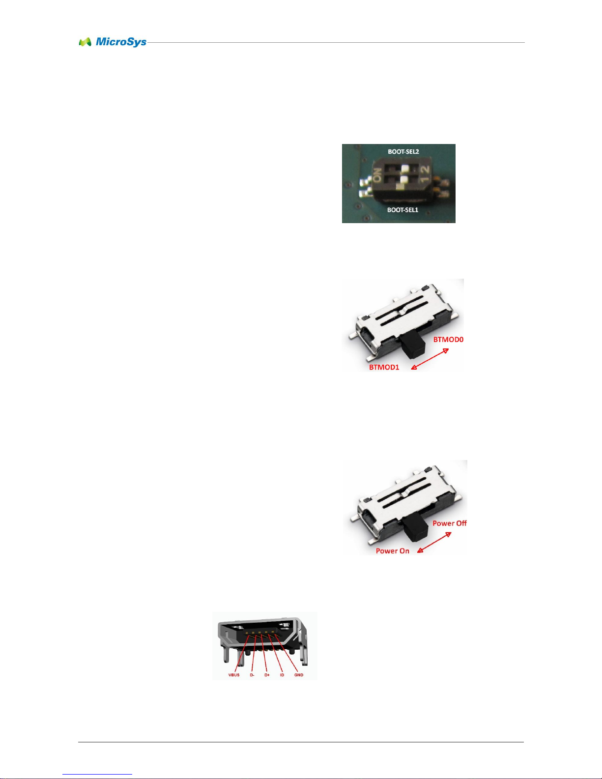
■ Make sure the switch BOOT, located on the CRX-S32V carrier board, is set
properly in order to select the correct boot source and board configuration.
For more details see chapter 5.3 Boot Mode Switch
■ Make sure the switch BMD, located on the MPX-S32V module, is set properly
in order to select the correct boot source.
For more details see chapter 5.2 Boot Mode Configuration
■ Make sure the switch GPU, located on the MPX-S32V module, is set properly
in order to select the correct GPU supply
For more details see chapter 6.5 Switches
■ The board comes preconfigured to boot correctly via SD-Card on arrival.
■ Connect the micro USB cable to USB.
Figure 1 BOOT Switch
Figure 4 USB Connector
Figure 2: BMD Switch
Figure 3: GPU Switch
Page 11
Quick Start Guide 3
miriac SBC-S32V User Manual
V 1.1
11/81
© MicroSys Electronics GmbH 2017
■ Connect other peripherals as far as intended.
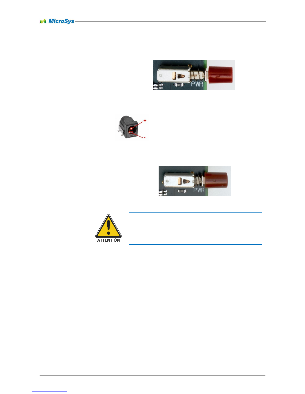
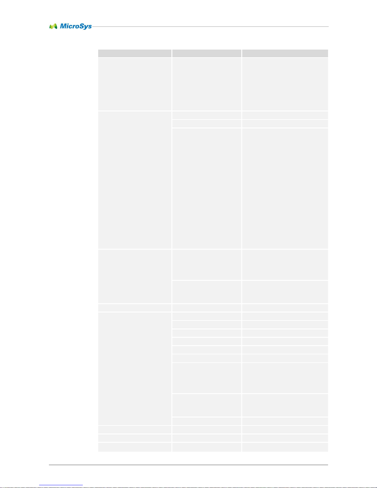
■ Make sure the power switch PWR is in off position (released)
■ Connect the 12V power line to the PWRA connector
■ Switch on the power by switch PWR
After Power-On, the green LED on the carrier should
light up.
IF NOT, DISCONNECT THE UNIT IMMEDIATELY FROM
THE POWER SOURCE AND CHECK FOR FAULTS!
Figure 6 Power Jack
Figure 7 Power Switch ON
Figure 5 Power Switch Off
Page 12

Quick Start Guide 3
miriac SBC-S32V User Manual
V 1.1
12/81
© MicroSys Electronics GmbH 2017
3.3 Operation
3.3.1 U-Boot Startup
When power is supplied the system will start.
On startup, U-Boot will come up similar to the following:
The exact output may vary, depending on U-Boot and MPX-S32V module versions in
use.
U-Boot 2016.01 (Aug 04 2017 - 09:06:53 +0200)
CPU: NXP S32V234 at 1000 MHz
Reset cause: unknown reset
Board: mpxs32v234-R2
I2C: ready
DRAM: 2 GiB
All (4) cores are up.
MMC: FSL_SDHC: 0
In: serial
Out: serial
Err: serial
Net: FEC
=>
Page 13

System Description 4
miriac SBC-S32V User Manual
V 1.1
13/81
© MicroSys Electronics GmbH 2017
4 System Description
This section describes all parts of the SBC-S32V system.
4.1 Block Diagram CRX-S32V Carrier
4.2 Block Diagram MPX-S32V Module
Page 14
System Description 4
miriac SBC-S32V User Manual
V 1.1
14/81
© MicroSys Electronics GmbH 2017
4.3 Feature Overview
Feature
Type
Description
CPU
NXP S32V234
CoreClock 1GHz
Quad-Cortex®-A53
Single-Cortex®-M4
SDRAM
Dual 32-bit DDR3L
interface
2 x up to 1GByte
up to 1066MT/s
Mass Storage
8-bit eMMC
16 GByte
PCI Express
miniPCIe Slot
Rev.2.0
5Gbps
Lane x1
RC/EP
100MHz Clock Source
I2C support
Removable Media
eSDHC-I / (eSDHC-II)
micro SD card holders
4bit support
Ethernet
RGMII
KSZ9031RN Phy
10/100/1000 BaseT
Link/ Activity Leds
Grahics Output
TFP410
HDMI Type A
DDC support
Video Input
MIPI-CSI-A
5V/12V supply
4 Lanes + Clock
27MHz Ref Clock
Mounting Holes
MIPI-CSI-B
5V/12V supply
4 Lanes + Clock
27MHz Ref Clock
Mounting Holes
Serial Interfaces
UART0
USB to serial Converter
USB-powered
micro USB Type B
UART1
LIN 2.1 interface
MC33662BLEF
CAN Interface
CAN-FD-1
TJA1051
120R Termination
CML Filter
ESD Protection
CAN-FD-2
TJA1051
120R Termination
CML Filter
ESD Protection
RTC
Time/Date
PCF85263A
2032 coin cell backup
Board Control
S9KEAZN64A
Voltage supervision
Reset logic
Boot configuration
Status led
Board Switches
Modul Switches
RCON/Serial Select
GPU Power Off
Page 15
System Description 4
miriac SBC-S32V User Manual
V 1.1
15/81
© MicroSys Electronics GmbH 2017
Feature
Type
Description
Carrier Switches
Power On/Off
Reset Button
Boot Mode 1
Boot Mode 2
CAN1 Termination On/Off
CAN2 Termination On/Off
Board Connectors
Modul Connectors
ADC Channel 0-7
MCU Programming Port
Carrier Connectors
12V Power Input
5V/12V Aux Power Out
5V/12V Fan Power Out
314 pin MXM Connector
microSD-A
microSD-B (not mounted)
miniPCIe
microUSB
RJ45 LAN
HDMI Out
MIPI-A
MIPI-B
CAN-A
CAN-B
LIN Interface
JTAG
Indicators
Module Leds
MCU Status
Reset Status
User GPIO1
User GPIO2
Carrier Leds
12V Power Indicator
User Led 1
User Led 2
Debug
JTAG
10 pin Header
Power Management
System On/Off
Pushbutton Switch
Input Voltage
12V DC
Input Current
typical. <1A, no loads
Supply Polarity
Reverse voltage protected
Overvoltage
TVS protected
Input Fuse
3A PPTC type
Module POL regulators
1.0V, max 10A
1.35V, max.6A
1.8V, max 3A
3.3V, max 3A
Carrier POL regulators
1.5V,max.3A
3.3V, max 3A
5.0V, max 3A
RTC Backup
2032 coin cell
Shielding
Connector Shield
connected to Ground
ESD Discharge
connected to Ground
Mechanics
Dimension
93x126mm
Page 16
System Description 4
miriac SBC-S32V User Manual
V 1.1
16/81
© MicroSys Electronics GmbH 2017
Feature
Type
Description
Module Mounting
4 Mountig Holes, 2.5mm Ø
all electrically floating
Carrier Mounting
4 Mountig Spacers, M2.5
2 Holes electrically floating
2 Holes electrically grounded
miniPCIe Mounting
2 Mounting Spacers, M2.5
all electrically grounded
MIPI-A Mounting
2 Mounting Holes, 3.2mm Ø
all electrically grounded
MIPI-B Mounting
2 Mounting Holes, 3.2mm Ø
all electrically grounded
Page 17
System Description 4
miriac SBC-S32V User Manual
V 1.1
17/81
© MicroSys Electronics GmbH 2017
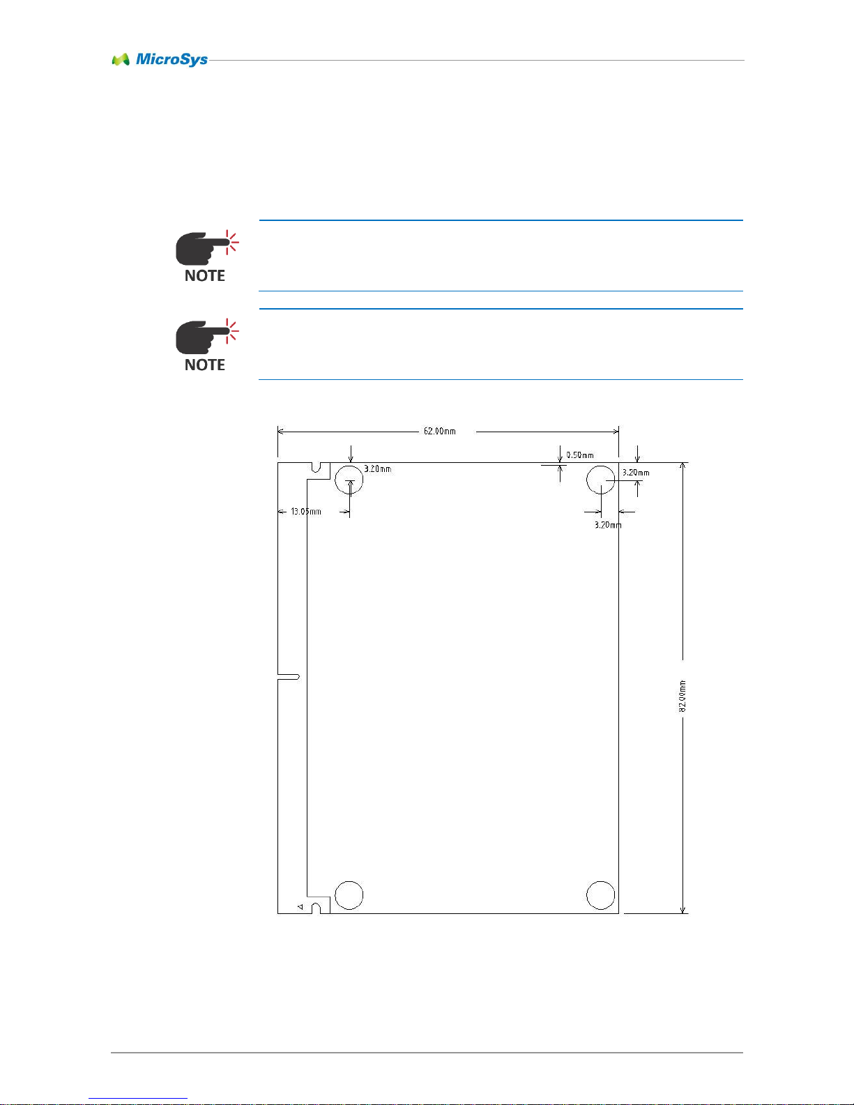
4.4 Mechanical Dimensions
4.4.1 MPX-S32V Module
The following drawing shows the mechanical outline of the MPX-S32V module that
is plugged in the CRX-S32V carrier board.
This drawing is not to scale.
For 3D data files please contact MicroSys.
Figure 8 Mechanical Dimensions
Page 18
System Description 4
miriac SBC-S32V User Manual
V 1.1
18/81
© MicroSys Electronics GmbH 2017
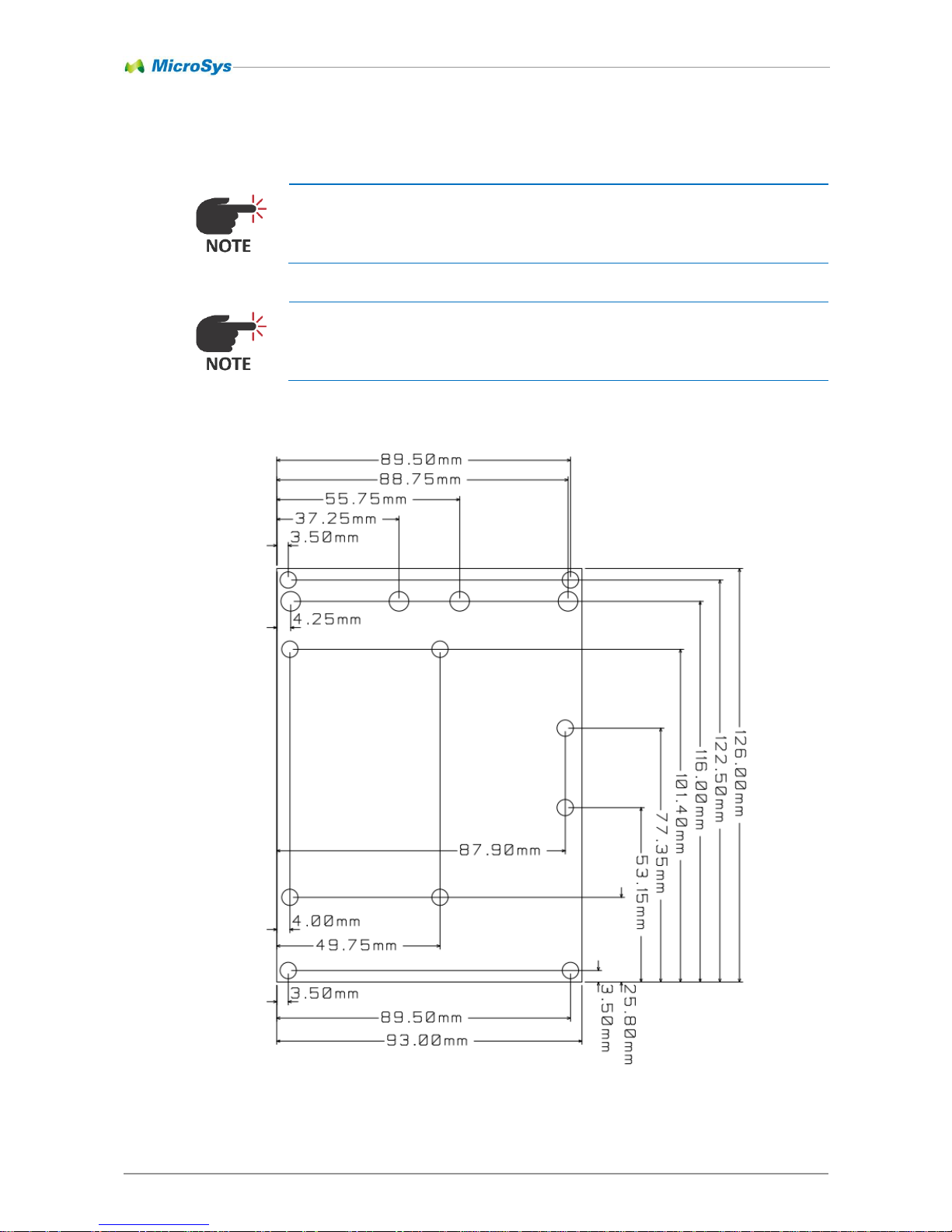
4.4.2 CRX-S32V Carrier
The following drawing shows the mechanical outline of the SBC-S32V assembly.
This drawing is not to scale.
For 3D data files please contact MicroSys.
Page 19
System Description 4
miriac SBC-S32V User Manual
V 1.1
19/81
© MicroSys Electronics GmbH 2017
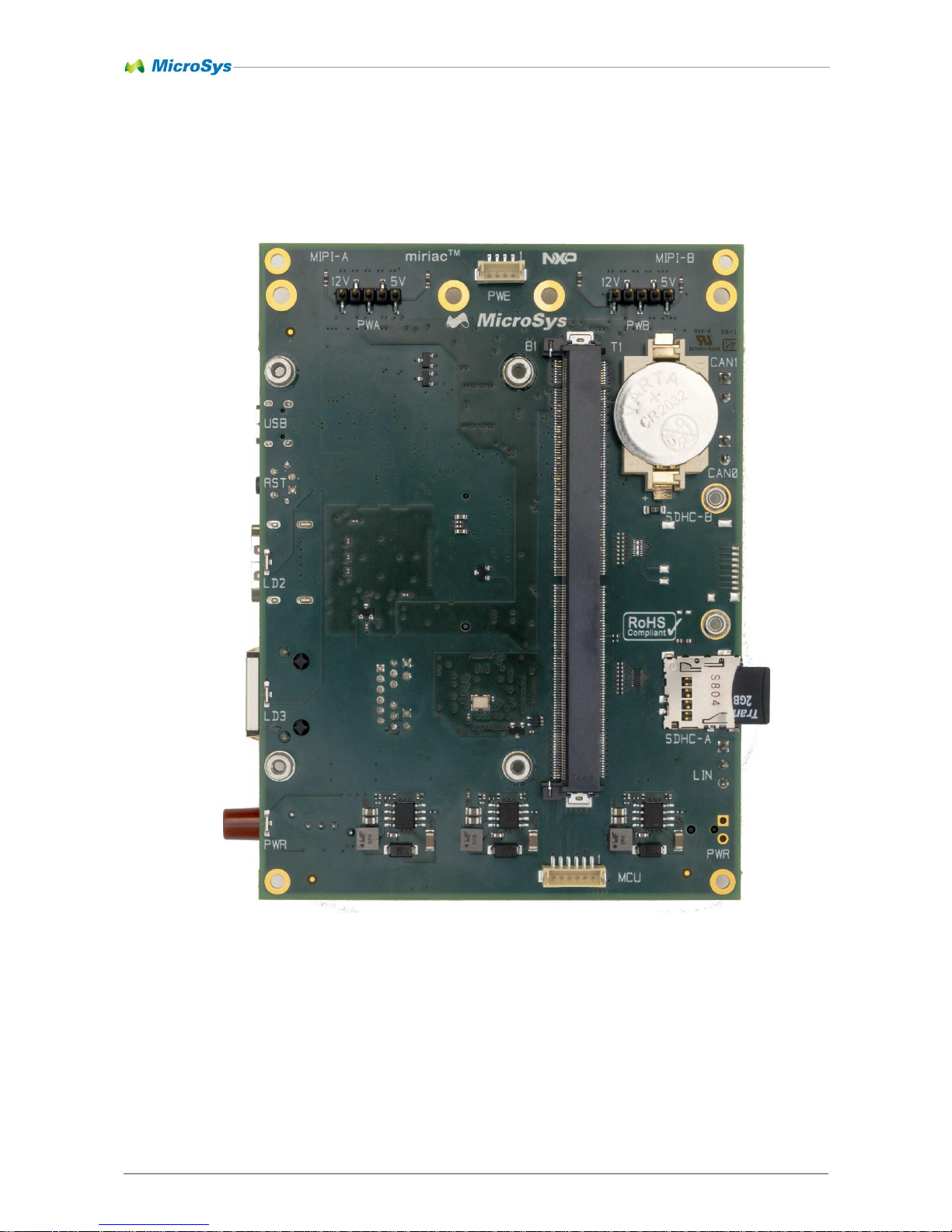
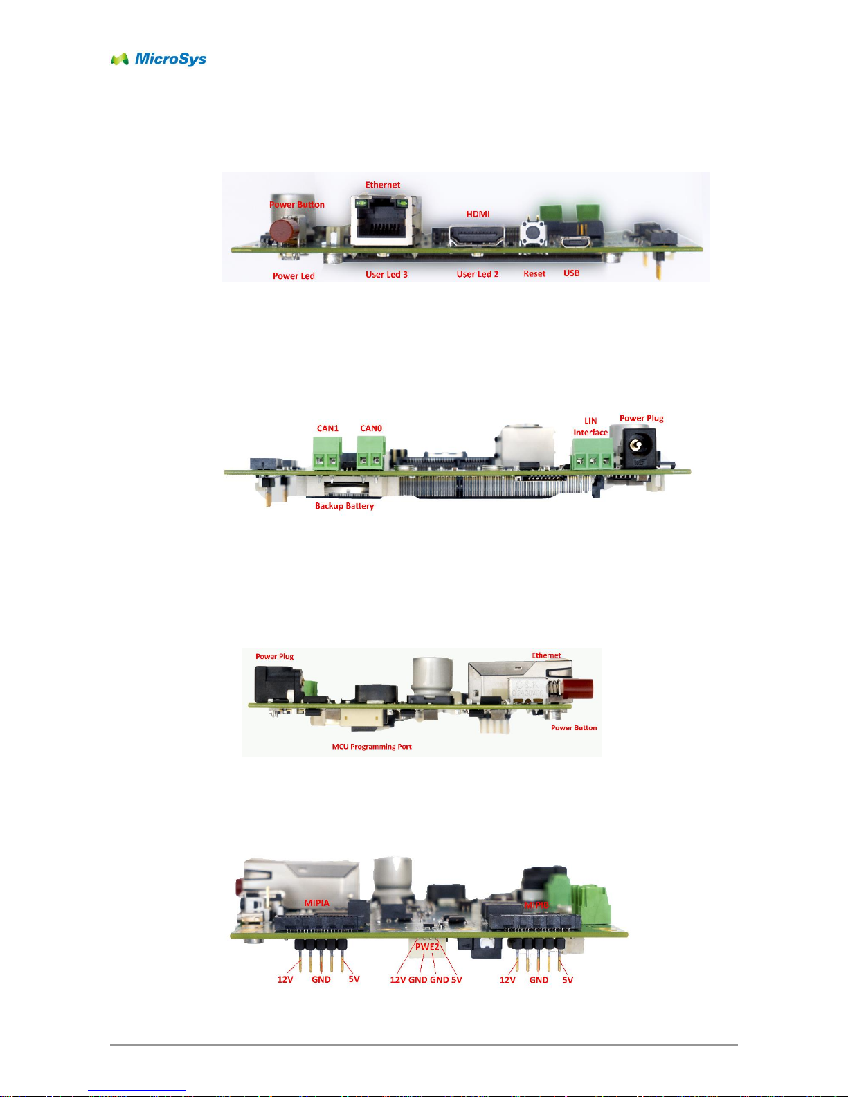
4.5 Carrier Board Layout – Module Side
Figure 9: Module Side connectors (carrier CRX-S32V)
Page 20
System Description 4
miriac SBC-S32V User Manual
V 1.1
20/81
© MicroSys Electronics GmbH 2017
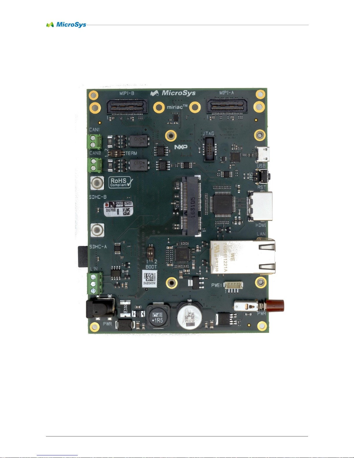
4.6 Carrier Board Layout – Non-Module Side
Figure 10 Non-Module Side connectors (carrier CRX-S32V)
Page 21
System Description 4
miriac SBC-S32V User Manual
V 1.1
21/81
© MicroSys Electronics GmbH 2017
4.7 Carrier Power Button Side View
4.8 Carrier Power Plug Side View
4.9 Carrier Bottom Side View
4.10 Carrier Top Side View
Page 22
System Description 4
miriac SBC-S32V User Manual
V 1.1
22/81
© MicroSys Electronics GmbH 2017
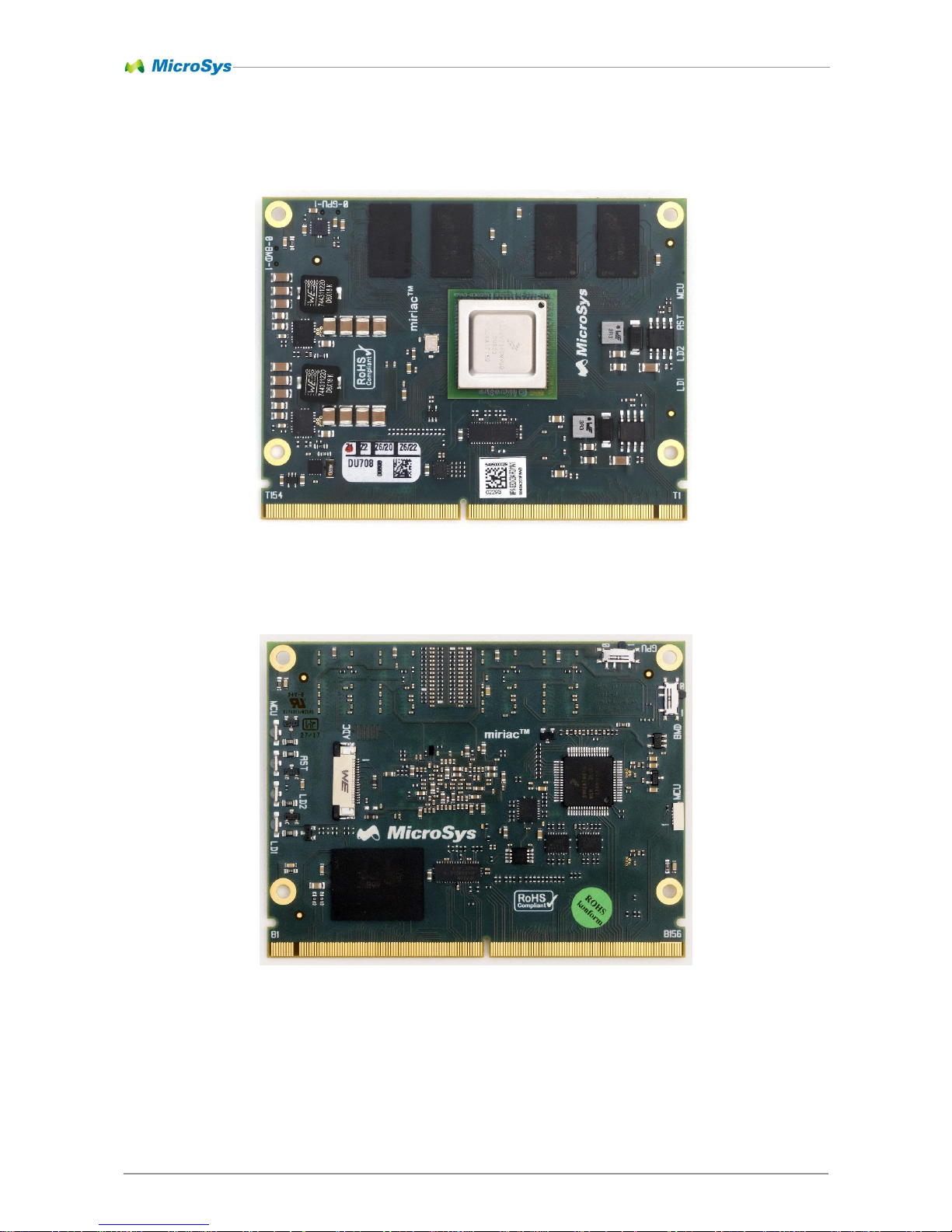
4.11 Module Top Side
4.12 Module Bottom Side
Page 23
System Description 4
miriac SBC-S32V User Manual
V 1.1
23/81
© MicroSys Electronics GmbH 2017
4.14 System Environment
4.14.1 Temperature Ratings
The SBC-S32V contains parts with the following ambient, junction or case
temperature ratings. Due to these limits, the system function is only guaranteed, if
none of them are exceeded at any time. The heatsink of the MPX-S32V requires
an adequate air flow, which can be accomplished by free or forced air convection.
If an active cooling is desired, a fan can be connected to one of the power
connectors PWE1 or PWE2, which provide +5.0V as well as +12V.
Part
Tmin
Tmax
BAT-CR2032MFR-1BL
-30°C
70°C
BAT-HOLDER-79527141
-55°C
85°C
C-0402-NP0-Series
-55°C
125°C
C-0402-X5R-Series
-55°C
85°C
C-0402-X7R-Series
-55°C
125°C
C-0603-226-X5R-Z
-55°C
85°C
C-0603-X7R-Series
-55°C
125°C
C-0805-X7R-Series
-55°C
125°C
C-1206-X7R-Series
-55°C
125°C
C-EEEFK1H331AQ
-55°C
105°C
CML-744-227
-40°C
125°C
CML-744-233-670
-40°C
85°C
D-B320A-13-F
-55°C
150°C
D-BAS70
-65°C
150°C
D-BAT54S
-55°C
125°C
D-SD2114S040S5R0
-55°C
125°C
FB-742-792-XXX
-55°C
125°C
HEADER-2.54-180-M-1X2
-40°C
125°C
HEADER-2.54-180-SM-1X5
-40°C
163°C
IC-BTS462T
-40°C
150°C
IC-DSC1001CI2-027.0000
-40°C
85°C
IC-DSC557-0344FI1
-40°C
85°C
IC-FT232RQ
-40°C
85°C
IC-IR347xMTRPBF
-40°C
125°C
IC-KSZ9031RNXIA
-40°C
85°C
IC-MAX4886ETO
-40°C
85°C
IC-MC33662BLEF
-40°C
125°C
IC-MT41K256M16HA-107-IT
-40°C
95°C
IC-MTFC16GAKAENA-4M-IT
-40°C
85°C
IC-NCV8715SQ50T2G
-40°C
125°C
Page 24
System Description 4
miriac SBC-S32V User Manual
V 1.1
24/81
© MicroSys Electronics GmbH 2017
Part
Tmin
Tmax
IC-PCA9517ADP
-40°C
85°C
IC-PCF85263ATL
-40°C
85°C
IC-PS32V234CMN0VUB
-40°C
125°C
IC-REF3030AIDBZ
-40°C
125°C
IC-S9KEAZN64AMLH
-40°C
85°C
IC-SN74LVC1G04DCK
-40°C
85°C
IC-SN74LVC1G125DCK
-40°C
125°C
IC-SN74LVC244ARGYR
-40°C
125°C
IC-TFP410PAP
0°C
70°C
IC-TJA1051T
-40°C
105°C
IC-TPS22920LYZP
-40°C
85°C
IC-TPS51200DRC
-40°C
85°C
IC-TPS5433xDDAR
-40°C
150°C
IC-TPS70933DBV
-40°C
125°C
L-744-311-220
-55°C
125°C
L-744-383-56033
-40°C
85°C
L-744-383-57068
-40°C
85°C
L-744-771-001
-55°C
125°C
LD-155124xx73200
-40°C
85°C
PCB-ADP-8065-01
-40°C
85°C
PCB-CRX-S32V-01
-40°C
85°C
PCB-MPX-S32V-02
-40°C
85°C
PTC-2920L330/24
-40°C
85°C
R-0402-Serie
-55°C
155°C
R-0603-Serie
-55°C
155°C
R-0805-Serie
-55°C
155°C
R-1206-Serie
-55°C
155°C
R-2010-Serie
-55°C
155°C
RC-IP4252CZ16-8
-40°C
85°C
ST-JAE-MM70-314-310-B1-1
-40°C
85°C
ST-JST-SM06B-XSRS-ETB
-25°C
85°C
ST-SAM-QSE-020-01-F-D
-55°C
125°C
ST-SAM-SHF-105-01-L-D-SM
-55°C
125°C
ST-TYCO-2041119-1-PCIe
-55°C
85°C
ST-WE-629-105-150-521
-40°C
85°C
ST-WE-679-30x-124-022
-25°C
85°C
ST-WE-685-119-134-923
-25°C
85°C
ST-WE-687-118-140-22
-25°C
85°C
ST-WE-691-214-110-00x
-40°C
105°C
ST-WE-694-106-106-102
-40°C
85°C
Page 25
System Description 4
miriac SBC-S32V User Manual
V 1.1
25/81
© MicroSys Electronics GmbH 2017
Part
Tmin
Tmax
ST-WE-749-911-1221A
0°C
70°C
ST-YE-PJS-008-2130-0
-25°C
85°C
SW-CK-G003R
-10°C
60°C
SW-CK-PN12SHSA03QE
-10°C
60°C
SW-WE-416-131-160-802
-40°C
85°C
SW-WE-431-256-038-716
-40°C
85°C
SW-WE-450-404-015-514
-40°C
85°C
T-BSS138LT1
-55°C
150°C
T-FDT434P
-55°C
150°C
T-PDTA114YT
-55°C
150°C
T-PDTC123JT
-65°C
150°C
TVS-1.5SMC15AT3
-65°C
150°C
TVS-ESD7504MUTAG
-55°C
125°C
TVS-PSOT36LC
-55°C
150°C
TVS-USBLC6-2P6
-40°C
125°C
XT-FT13A-xx.00000/8-20-20/48
-40°C
85°C
XT-FT26A-32.7680/12.5-20/48
-40°C
85°C
Y-WE-977-403-0151-M25-3MM00
-55°C
125°C
4.14.2 Power Dissipation
Component
max.Temperature
Power Dissipation
CPU
Tj125° C
7W
DDR
Tc95° C
1.5W
Core Regulator
Tj125° C
1.2W
DDR Regulator
Tj125° C
0.3W
eMMC
Ta85° C
0.5W
LAN
Tj125° C
0.9W
HDMI
Ta70° C
0.9W
(j=junction, c=case, a=ambient)
Page 26

System Description 4
miriac SBC-S32V User Manual
V 1.1
26/81
© MicroSys Electronics GmbH 2017
4.15 Power Supply
4.15.1 Input Supply Rating
The SBC-S32V system is run from a single power supply with the following ratings:
Input Voltage Operating Range:
12V DC +/-5%
Typical Current Consumption
(@12V / room temperature / U-boot prompt):
0,40A
The input of the SBC-S32V system is protected against wrong polarity and over
current
DO NOT exceed the rated maximum values for the power
supply! This may result in severe permanent damage to
the unit, as well as possible serious injury.
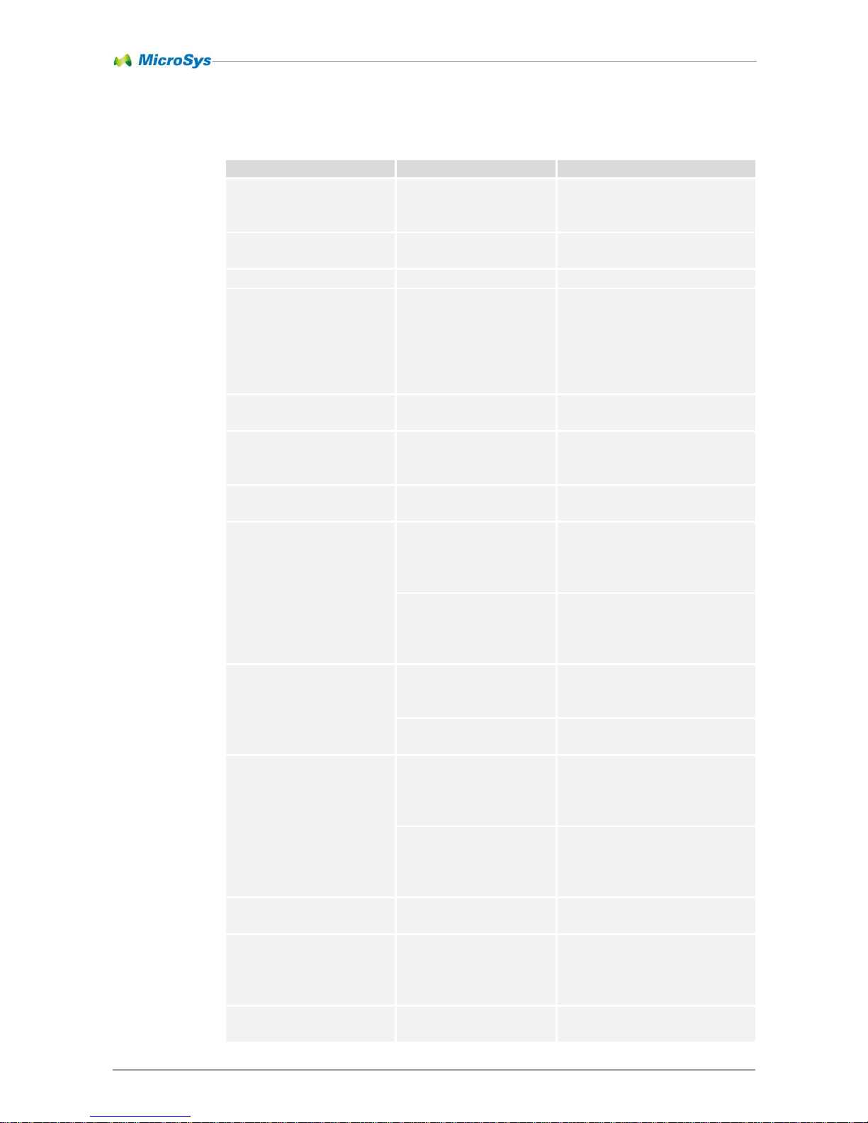
4.15.2 Input Power Connector
Power is fed to the unit via the 2-pin DC power jack PWRA
Manufacturer:
Würth Elektronik
Type:
694-106-106-102
Mates with:
dc power plug 5.5mm x 2.5mm
Figure 4-6 Power Jack
Page 27

System Description 4
miriac SBC-S32V User Manual
V 1.1
27/81
© MicroSys Electronics GmbH 2017
4.15.3 Input Power Switch
The unit can be switch on and off by a push button switch. The switch controls all
on system supply rails via a high side power switch. The silicon switch has a
nominal load current of 3.5A, an on-state resistance of 100mR and it is fully
protected against current and thermal overload.
The push button switch has two alternate positions, i.e. pressed and released. The
position of the switch sets the power state of the SBC-S32V system. It will not be
reset, in case the power cord is disconnected. The switch can be optionally
equipped with various switch caps in form and color
Manufacturer:
C&K-Components
Type:
PN12SHSA03QE
Mates with:
G001/2/3/4-A/G/I/R
Figure 12: G003-
Series
Figure 11:PN12SHSA03QE
Page 28

System Description 4
miriac SBC-S32V User Manual
V 1.1
28/81
© MicroSys Electronics GmbH 2017
4.15.4 Fuses
There is a PPTC fuse on the SBC-S32V.
The part is a self-resettable fuse with a nominal current rating of 3.3A at 20°C
ambient temperature. The current is derated due to the ambient temperature
according to the following table:
-40°C
-20°C
0°C
20°C
40°C
50°C
60°C
70°C
85°C
4,7A
4,2A
3,8A
3,3A
2,9A
2,6A
2,3A
1,9A
1,6A
4.15.5 Power Supply Structure
Figure 4-7 Fuse Derating
Figure 13 Power supply structure
Page 29

System Description 4
miriac SBC-S32V User Manual
V 1.1
29/81
© MicroSys Electronics GmbH 2017
4.15.6 Power Distribution
There are two power connectors available onboard the SBC-S32V. These 4 pin
shrouded header connectors can be used to connect an external fan or for
additional supply voltages required for miniPCIe modules. The current rating is
limited to 1A per pin. The voltages are switched on and off by the main power
switch. The +12V voltage is sourced by the input voltage, which is derated by
maximal 550mV, caused by the input polarity protection diode. An external load
must no feed in any reverse current or voltage during any power state, f.e. an
external inductive load must be equipped with a freewheeling circuit.
Manufacturer:
Würth
Type:
679304124022
mates with:
648004113322
Figure 14: Connector PWE1 & PWE2
Page 30

System Description 4
miriac SBC-S32V User Manual
V 1.1
30/81
© MicroSys Electronics GmbH 2017
4.15.7 MIPI Power
The two MIPI ports of the SBC-S32V system can be either work with 5.0V only or
mixed with +5.0V and +12V. This option is handled by two 5 pin 2.54mm headers.
Manufacturer:
Fischerelektronik
Type:
SL10SMD0525G
mates with:
2.54mm Jumper Link
PWA
Signal
Description
1
+5.0V
Power Rail
2
VCCA
Supply for MIPIA Pin 25 & 27
3
GND
Ground
4
VCCA
Supply for MIPIA Pin 25 & 27
5
+12V
Power Rail
PWB
Signal
Description
1
+5.0V
Power Rail
2
VCCB
Supply for MIPIB Pin 25 & 27
3
GND
Ground
4
VCCB
Supply for MIPIB Pin 25 & 27
5
+12V
Power Rail
In case the pins 25 and 27 should not be powered, no link at all should be installed.
If these pins should be grounded, a link between pin 2 and 3 or 3 and 4 must be
set.
Anyway, only a single link per header must be set at a
time. More than one link installed may cause permanent
damage to the board!
Figure 15: Header PWA & PWB
Page 31

System Description 4
miriac SBC-S32V User Manual
V 1.1
31/81
© MicroSys Electronics GmbH 2017
4.15.8 Power Up
During a power up sequence, the MCU first checks the input voltage to be within
their necessary limits. After that, the POL (Point Of Load) regulators on the module
will be activated as well as the tracking regulators for 5V, 3.3V and 1.5V on the carrier board. If all module voltages are o.k. the reset sequence will be started. If there
is no external reset request, f.e. via RSTIN# from the reset key, the RESET# will be
released after 100ms. A low level on the RSTIN# line extends this time. During normal operation, a falling edge at RSTIN# initiates a reset sequence for the whole
system, which is at least 100ms long. As long the reset key is pressed, the system
will be held in the reset state. If the key is released, the CPU will fetch its power up
configuration and starts up with its BIST and/or boot sequence. The RSTOUT# sig-
nal will directly follow the state of the RESET# signal. As long the RSTOUT# is
active all connected devices must be held in a reset state in order not to block the
power up configuration settings.
+12V
PWEN
V(intern)
RSTIN#
RSTOUT#
PORST#
In case the MCU detects any overvoltage, it will turn off all internal point of load
regulators. The external supply voltage is reverse polarity protected and limited by
a 15V transient voltage suppressor diode to protect the system. The input poly fuse
is rated for a maximum voltage of 24V, i.e. any voltage above that limit will destroy
the input protection of the system.
Page 32

System Description 4
miriac SBC-S32V User Manual
V 1.1
32/81
© MicroSys Electronics GmbH 2017
4.16 Reset Structure
Signal Name
Function
Type
RSTIN#
System Global Reset Input
4K7 Pullup
RSTOUT#
System Global Reset Output
Totem Pole
PORST#
Power-On Reset for CPU
Totem Pole
RESET#
Reset for CPU
Open Drain
FRSTI#
Reset for eMMC device
Totem Pole
M0RST#
Reset for Memory Bank 0
Totem Pole
M1RST#
Reset for Memory Bank 1
Totem Pole
( # denotes an active low signal )
Table 4-3 Reset signal overview
Figure 4-3 Reset Structure
Page 33

System Core, Boot Configuration 5
miriac SBC-S32V User Manual
V 1.1
33/81
© MicroSys Electronics GmbH 2017
5 System Core, Boot Configuration
5.1 Processor NXP S32V234
The S32V234 is a vision processing MPU with four ARM® Cortex®-A53 cores and
a single Cortex-M4 core. The four CPU cores run at a maximum clock speed of
1000MHz.
Figure 4-7 Processor Block diagram
Page 34

System Core, Boot Configuration 5
miriac SBC-S32V User Manual
V 1.1
34/81
© MicroSys Electronics GmbH 2017
5.2 Boot Mode Configuration
The SBC-S32V board offers several different boot modes to choose from. The settings can be done via the sliding switch BMD on the module and the dipswitch
BOOT on the carrier according to following table.
The switch BMD sets the BMODE[0] and BMODE[1] signals of the CPU to low,
while the two configuration resistors BMD0 and BMD1 are used to set a fixed low
value on these lines.
The parts BMD, BMD0 and BMD1 are located on the MPX-S32V module.
green denotes the default configuration
Note 1) BMD0 and BMD1 are soldered resistors (size 0402) and not intended to be
changed by user.
Shown positions set the according BTMOD0/1 line to low. BTMOD0 controls the
CPU configuration port PC9, i.e. BOOTMOD(0), while BTMOD1 is connected to the
CPU configuration port PC10, i.e. BOOTMOD(1).
Boot Mode
BMD-Switch
BMD01)
BMD11)
Serial Download, virgin device
No function
installed
installed
Serial Download, virgin device
Position 0
removed
installed
Serial Download, prog. device
Position 1
removed
installed
RCON Boot, if no fuses
Position 0
installed
removed
Serial Download, prog. device
Position 1
installed
removed
RCON Boot, no fuses
Position 0
removed
removed
Serial Download, prog. device
Position 1
removed
removed
Figure 16: BMD Switch
Figure 18: Position BTM1=low
Figure 17: Position BTM0=low
Page 35

System Core, Boot Configuration 5
miriac SBC-S32V User Manual
V 1.1
35/81
© MicroSys Electronics GmbH 2017
5.3 Boot Mode Switch
The boot mode switch BOOT located on the CRX-S32V, allows the following default boot modes, in case the BMD switch is set to position RCON. If the BMD
switch is set to serial download, the BOOT switch has no function.
Setting
BOOT-SEL1
BOOT-SEL2
Boot Device
OFF
OFF
Cortex A53 via SDHC-A
ON
OFF
Cortex A53 via eMMC
OFF
ON
Cortex M4 via SDHC-A
ON
ON
Cortex M4 via eMMC
green denotes the default configuration
In case, the eMMC or the SDHC-Slot should be used after a boot from the other
device, the Boot Mode Switch 1 must be set to either position and the “MMC
RESCAN” command must be executed within u-boot. The “MMC INFO” command
will then show the new active storage device.
Figure 19: Boot Mode Switch
Page 36

System Core, Boot Configuration 5
miriac SBC-S32V User Manual
V 1.1
36/81
© MicroSys Electronics GmbH 2017
5.4 Power Up Configuration
The S32V234 is configured during power up by the state of 32 I/O signals, which
are controlled by the MCU. Within the MCU, the four most popular RCON boot
configurations are implemented and can be selected via the dip-switch BOOT
placed on the carrier board.
These configurations are only valid, if the Boot Mode Configuration is set to RCON Boot!
Signal
RCON
Port
eSDHC Mode
eMMC Mode
FLXR-TENB
RCON[0]
PA[7] 0 0
FLXR-TXD
RCON[1]
PA[8] 0 0
FLXR-RXD
RCON[2]
PA[9] 0 0
UART0-RXD
RCON[3]
PA[11] 0 0
UART0-TXD
RCON[4]
PA[12] 0 1
UART1-RXD
RCON[5]
PA[13] 0 0
UART1-TXD
RCON[6]
PA[14] 0 1
I2C0-SDA
RCON[7]
PA[15] 1 1
I2C0-SCL
RCON[8]
PB[0] 0 0
I2C1-SDA
RCON[9]
PB[1] 0 0
I2C1-SCL
RCON[10]
PB[2] 0 0
I2C2-SDA
RCON[11]
PB[3] 0 1
SPI0-SCK
RCON[12]
PB[5] 0 0
SPI0-SOUT
RCON[13]
PB[6] 0 0
SPI0-SIN
RCON[14]
PB[7] 0 0
SPI0-CS0#
RCON[15]
PB[8] 0 1
SPI1-SCK
RCON[16]
PB[9] 0 1
SPI1-SOUT
RCON[17]
PB[10] 0 0
SPI1-SIN
RCON[18]
PB[11] 0 0
SPI1-CS0#
RCON[19]
PB[12] 0 0
SPI2-SCK
RCON[20]
PB[13] 0 0
SPI2-SOUT
RCON[21]
PB[14] 1 1
SPI2-SIN
RCON[22]
PB[15] 0 0
SPI2-CS0#
RCON[23]
PC[0] 0 0
SPI3-SCK
RCON[24]
PC[1] 0 0
SPI3-SOUT
RCON[25]
PC[2] 0 0
SPI3-SIN
RCON[26]
PC[3] 0 0
SPI3-CS0#
RCON[27]
PC[4] 0 0
FXT0-CH0
RCON[28]
PC[5] 0 0
FXT0-CH1
RCON[29]
PC[6] 0 0
FXT0-CH2
RCON[30]
PC[7] 0 0
FXT0-CH3
RCON[31]
PC[8] 1 1
Page 37

System Core, Boot Configuration 5
miriac SBC-S32V User Manual
V 1.1
37/81
© MicroSys Electronics GmbH 2017
5.5 MCU programming Port
The MCU, a Kinetis S9KEAZN64AMLH, controls the power on and the reset
sequence. It monitors all module generates supply voltages and drives all
configuration lines of the S32V234 CPU. The controller can be either programmed
via a module connector or a connector on the carrier board, both named MCU. As
the module connector is very tiny and has a pitch of 0.6mm, the carrier located
connector with its 1.5mm pitch should be preferred.
MPX-S32V Connector MCU
Manufacturer:
JST
Type:
SM06B-XSRS-ETB
mates with:
06XSR-36S
Figure 20: Module MCU Connector
Page 38

System Core, Boot Configuration 5
miriac SBC-S32V User Manual
V 1.1
38/81
© MicroSys Electronics GmbH 2017
The module connector is supplied by the direct MCU supply with 3.3V, while the
+3.3V supply of the carrier located connector is derived from a carrier located
supply, which can be disabled by the MCU. If the MCU has configured the board
with PWEN off, no supply is available on the carrier and its connectors. In this case
the module connector must be used for programming or the IO voltage of the
programmer is externally set to 3.3V.
CRX-S32V Connector MCU
Manufacturer:
Würth
Type:
679306124022
mates with:
648006113322
Figure 21: Carrier MCU Connector
Page 39

System Core, Boot Configuration 5
miriac SBC-S32V User Manual
V 1.1
39/81
© MicroSys Electronics GmbH 2017
5.5.1 MCU Pinout
MCU
Board
S32V234
Function
Pin
Port
Dir
Signal
Signal
RCON
1
PTD1
Out
BCFG23
SPI2_CS0#
RCON[23]
Configuration
2
PTD0
Out
BCFG29
FXT0_CH1
RCON[29]
Configuration
3
PTH7
Out
BCFG22
SPI2_SIN
RCON[22]
Configuration
4
PTH6
Out
BCFG6
UART1_TXD
RCON[6]
Configuration
5
PTE7
Out
RSTOUT#
Modul Rest Output
6
PTH2 n.c.
not connected
7 In
+3V3
Supply
8 In
VREFH
+3.0V
9 In
VREFL
Reference Ground
10
GND
Reference Ground
11
PTB7
Out
FRSTI#
eMMC Reset
12
PTB6
Out
PWEN
PSU enable
13
GND
Reference Ground
14
PTH1
In
QSPI-SEL
GPIO[158]
FLASH/SDHC Mux
15
PTH0
IO
TRTC#
Time Stamp RTC
16
PTE6
In
IRTC#
Interrupt RTC
17
PTE5
Out
PORST#
EXT_POR#
PowerOnReset
18
PTB5
Out
RESET#
RESET# Reset
19
PTB4
In
FCCU-F0
FCCU_F0
Failure Check&Correction
20
PTC3
In
LD4
yellow Led
21
PTC2
In
+3V3
ADC Divider 3:4
22
PTD7
Out
NMI
NMI Interrupt
23
PTD6
Out
FCCU-F1
FCCU_F1
Failure Check&Correction
24
PTD5
OUT
BCFGE#
Configuration Enable
25
PTC1
In
+3.3V
ADC Divider 3:4
26
PTC0
In
+1.8V
ADC direct
27
PTF7
In
+1.35V
ADC direct
28
PTF6
In
+1.0V
ADC direct
29
PTF5
In
+VIN
ADC Divider 1:11
30
PTF4
Out
BCFG2
FLXR_RXD
RCON[2]
Configuration
31
PTB3
Out
BCFG0
FLXR_TENB
RCON[0]
Configuration
32
PTB2
Out
BCFG1
FLXR_TXD
RCON[1]
Configuration
33
PTB1
Out
BCFG3
UART0_RXD
RCON[3]
Configuration
34
PTB0
Out
BCFG4
UART0_TXD
RCON[4]
Configuration
35
PTF3
Out
BCFG7
I2C0_SDA
RCON[7]
Configuration
36
PTF2
Out
BCFG8
I2C0_SCL
RCON[8]
Configuration
37
PTA7
Out
BCFG9
I2C1_SDA
RCON[9]
Configuration
38
PTA6
Out
BCFG10
I2C1_SCL
RCON[10]
Configuration
39
PTE4
Out
BCFG14
SPI0_SIN
RCON[14]
Configuration
40
GND
Reference Ground
Page 40

System Core, Boot Configuration 5
miriac SBC-S32V User Manual
V 1.1
40/81
© MicroSys Electronics GmbH 2017
MCU
Board
S32V234
Function
41 In
+3V3
Supply
42
PTF1
Out
BCFG15
SPI0_CS0#
RCON[15]
Configuration
43
PTF0
Out
BCFG12
SPI0_CLK
RCON[12]
Configuration
44
PTD4
Out
BCFG13
SPI0_SOUT
RCON[13]
Configuration
45
PTD3
Out
BCFG24
SPI3_CLK
RCON[24]
Configuration
46
PTD2
Out
BCFG5
UART1_RXD
RCON[5]
Configuration
47
PTA3
Out
BCFG25
SPI3_SOUT
RCON[25]
Configuration
48
PTA2
Out
BCFG18
SPI1_SIN
RCON[18]
Configuration
49
PTA1
Out
BCFG17
SPI1_SOUT
RCON[17]
Configuration
50
PTA0
Out
BCFG31
FXT0_CH3
RCON[31]
Configuration
51
PTC7
Out
BCFG26
SPI3_SIN
RCON[26]
Configuration
52
PTC6
Out
BCFG30
FXT0_CH2
RCON[30]
Configuration
53
PTE3
Out
BCFG11
I2C2_SDA
RCON[11]
Configuration
54
PTE2
Out
BCFG16
SPI1_CLK
RCON[16]
Configuration
55
PTG3
Out
BCFG19
SPI1_CS0#
RCON[19]
Configuration
56
PTG2
Out
BCFG21
SPI2_SOUT
RCON[21]
Configuration
57
PTG1
Out
BCFG28
FXT0_CH0
RCON[28]
Configuration
58
PTG0
Out
BCFG27
SPI3_CS0#
RCON[27]
Configuration
59
PTE1
Out
BCFG20
SPI2_CLK
RCON[20]
Configuration
60
PTE0
In
BOOT-SEL1
Boot Mode
61
PTC5
In
BOOT-SEL2
Boot Mode
62
PTC4
In
MCU-CLK
Programming Interface
63
PTA5
In
RSTIN#
Programming Interface
64
PTA4
IO
MCU-DIO
Programming Interface
Page 41

MPX-Module 6
miriac SBC-S32V User Manual
V 1.1
41/81
© MicroSys Electronics GmbH 2017
6 MPX-Module
The MPX-S32V miriac module fits in the MXM connector of the CRX-S32V carrier
board. It must be mounted with a heatsink and is fixed with 4 Torx screws M2.5x16.
The SBC-S32V is designed to stand in an upright position with the two MIPI
camera connectors on top and the heatsink as vertical support.
The recess at the bottom of the heatsink allows for an access to the MCU
programming port.
In case, an active cooling is desired, the top middle connector PWE2 provides
+5.0V and +12V.
All other connections and controls are located on the left and right vertical side of
the system.
Page 42

MPX-Module 6
miriac SBC-S32V User Manual
V 1.1
42/81
© MicroSys Electronics GmbH 2017
6.1 Mounting/Unmounting
The mounting or unmounting of the module should only be made in a static free
area with full ESD precautions, i.e. as a minimum, a grounded dissipative work
surface of sufficient size and a grounded skin contact wrist strap are necessary.
Make sure, that all parts, the carrier, the module and the heatsink are placed on the
same static free area to avoid any discharges between them during assembly.
To mount the MPX-S32V module, make sure that the carrier is disconnected from
any power or other IO interfaces. Both connector surfaces of the module must be
clean as well as the carrier connector should be checked for bent or dirty contacts.
Check the module and the carrier for foreign or loose parts, which do not belong to
the boards. The screws should have clean threads and be tightened with a
maximum torque of 30Ncm.
Insert or remove the MPX-S32V module always by an angle of about 25° like
shown in the following figure.
The thermal conduction between cooler and CPU is performed via a 1mm thick
thermal pad. Make sure, that this thermal pad is placed over the CPU package
before mounting the heatsink.
Page 43

MPX-Module 6
miriac SBC-S32V User Manual
V 1.1
43/81
© MicroSys Electronics GmbH 2017
After the module has been pressed down, place the heatsink exactly over the
mounting holes without scratching or touching any other parts on the PCB.
Insert the outer screws first and tighten them just a few turns. Then insert the two
inner screws also with a few turns. Now check the gap between carrier and module
for other parts than the CPU touching the heatsink. Check the thermal CPU pad for
correct position. Tighten the four screws with no more than 30Ncm.
For the removal of the module, first unplug all connections to the system. Take off
the inner screws, then the outer ones. The thermal pad may cause the heatsink
sticking to the module, so take care, while pulling apart to avoid collisions with any
part of the module. Lift the module to about 25°and remove it from the connector.
Store the parts on a static free area.
Page 44

MPX-Module 6
miriac SBC-S32V User Manual
V 1.1
44/81
© MicroSys Electronics GmbH 2017
6.2 DRAM
The module is fitted with two individual DDR3L memory blocks, each 32bits wide
and with 1GByte capacity. The used parts are 4GBit devices organized in 256M x
16 bits with 15 row, 10 column and 3 bank addresses. The refresh rate depends on
the operating temperature must be set according to the following table
Case Temperature
Refresh Cycle Time
Tc<85°C
7.8us
85°C<Tc<95°C
3.9us
95°C<Tc<105°C
1.95us
The DDR3L command bus is actively terminated and the routed in a fly by
structure. The following table shows all trace lengths, in case write leveling should
be adjusted. The used layer stack together with the FR4 material causes a signal
run time of 6.8ps/mm.
DRAM
Signal Group
Trace Length
Description
Bank0
Command
J1->J2
54.0mm
CPU->DRAM
Bank0
Command
J2->J3
13.1mm
DRAM->DRAM
Bank0
Byte 0
J1->J2
25.7mm
CPU->DRAM
Bank0
Byte 1
J1->J2
22.7mm
CPU->DRAM
Bank0
Byte 2
J1->J3
23.1mm
CPU->DRAM
Bank0
Byte 3
J1->J3
18.3mm
CPU->DRAM
Bank1
Command
J1->J4
54.5mm
CPU->DRAM
Bank1
Command
J4>J5
13.9mm
DRAM->DRAM
Bank1
Byte 0
J1->J4
25.3mm
CPU->DRAM
Bank1
Byte 1
J1->J4
22.9mm
CPU->DRAM
Bank1
Byte 2
J1->J5
19.0mm
CPU->DRAM
Bank1
Byte 3
J1->J5
17.2mm
CPU->DRAM
Page 45

MPX-Module 6
miriac SBC-S32V User Manual
V 1.1
45/81
© MicroSys Electronics GmbH 2017
6.3 eMMC
The local boot device of the MPX-S32V module is realized as an eMMC. The
MTFC16GAKAENA-4M-IT from Micron uses the 8-bit wide data bus, provided by
the µSDHC module of the S32V234. This interface is shared between the external
storage devices on the carrier board and the local eMMC. The selection can be
either made by the setting of a CPU GPIO pin or via the MCU. Per default, the
multiplexing is done through the MCU by the setting of the boot mode switch.
The reset input of the eMMC device is connected to port PTB7 of the MCU. In case
this port is not configured, the FRSTI# signal is tied to +3.3V by a pullup resistor.
6.4 Leds
There are four LEDs onboard the MPX-S32V module. The user LEDs 1 and 2 can
be controlled by two CPU GPIO pins, led 3 indicates state of the reset line and led
4 is connected to the MCU port PTC3.
Led
Color
ON
OFF
Description
LD1
green
CPU-PG5=high
CPU-PG5=low
LDG1 installed / LDG3 not installed
LD2
green
CPU-PG6=high
CPU-PG6=low
LDG2 installed / LDG4 not installed
LD1
green
CPU-PB1=high
CPU-PB1=low
LDG3 installed / LDG1 not installed
LD2
green
CPU-PB2=high
CPU-PB2=low
LDG4 installed / LDG2 not installed
LD3
red
RESET#=low
RESET#=high
Reset state indicator
LD4
yellow
MCU-PTC3=high
MCU-PTC3=low
MCU status led
Figure 22: MPX-LEDs
Page 46

MPX-Module 6
miriac SBC-S32V User Manual
V 1.1
46/81
© MicroSys Electronics GmbH 2017
6.5 Switches
The sliding switch GPU on the MPX-S32V module is used to disconnect the GPU
power pins to reduce power consumption, in case the GPU is not used. The other
sliding switch BMD is used to select between RCON controlled and serial boot
mode. Both switches are located at the PCB edge on the bottom of the MPX-S32V
module.
Any handling of these switches must be done exclusively using
nonconductive tools to avoid short circuits between carrier
board and module.
Figure 23: GPU switch
Figure 26: BMD Switch
Figure 25: GPU Power On (default)
Figure 24: GPU Power Off
Page 47

MPX-Module 6
miriac SBC-S32V User Manual
V 1.1
47/81
© MicroSys Electronics GmbH 2017
6.6 Module Connector
The carrier board CRX-S32V provides a connector “MXM” which accepts only
compatible CPU modules from the MicroSys MPX-S32V-family.
Manufacturer:
JAE
Type:
MM70-314-310-B1-1-R300
Used with:
MicroSys MPX-S32V module family
Figure 27: MXM-Connector
Page 48

MPX-Module 6
miriac SBC-S32V User Manual
V 1.1
48/81
© MicroSys Electronics GmbH 2017
6.7 Module/Carrier Connections
MPX-S32V
IO
CRX-S32V
Pin
Signal
Voltage
Pin
Signal
B1
IIC1-SDA
3.3V
B1
CSI1-SDA (MIPIB)
T1
GND
T1
GND
B2
GND
B2
GND
T2
CAN-FD0-TX
3.3V
T2
CAN-FD0-TX (CAN0)
B3
IIC1-SCL
3.3V
B3
CSI1-SCL (MIPIB)
T3
CAN-FD0-RX
3.3V
T3
CAN-FD0-RX (CAN0)
B4
JTAG-TCK
3.3V
B4
JTAG-TCK (JTAG)
T4
GND
T4
GND
B5
JTAG-TDI
3.3V
B5
JTAG-TDI (JTAG)
T5
CAN-FD1-TX
3.3V
T5
CAN-FD1-TX (CAN1)
B6
JTAG-TRST#
3.3V
B6
JTAG-TRST# (JTAG)
T6
CAN-FD1-RX
3.3V
T6
CAN-FD1-RX (CAN1)
B7
JTAG-TMS
3.3V
B7
JTAG-TMS (JTAG)
T7
GND
T7
GND
B8
GND
B8
GND
T8
CSI1-DT0+
1.0V
T8
CSI1-DT0+ (MIPIB)
B9
JTAG-TDO
3.3V
B9
JTAG-TDO (JTAG)
T9
CSI1-DT0-
1.0V
T9
CSI1-DT0- (MIPIB)
B10
FLXR-TENB
3.3V
B10
FLXR-TENB (CAN1)
T10
GND
T10
GND
B11
FLXR-TENA
3.3V
B11
FLXR-TENA (CAN0)
T11
CSI1-DT1-
1.0V
T11
CSI1-DT1- (MIPIB)
B12
FLXR-TXD
3.3V
B12
FLXR-TXD (LED2)
T12
CSI1-DT1+
1.0V
T12
CSI1-DT1+ (MIPIB)
B13
FLXR-RXD
3.3V
B13
FLXR-RXD (LED3)
T13
GND
T13
GND
B14
GND
B14
GND
T14
CSI1-DT2+
1.0V
T14
CSI1-DT2+ (MIPIB)
B15
3.3V rail output
B15
+3V3
T15
CSI1-DT2-
1.0V
T15
CSI1-DT2- (MIPIB)
B16
1.8V rail output
B16
+1V8
T16
GND
T16
GND
B17
GND
B17
GND
T17
CSI1-DT3-
1.0V
T17
CSI1-DT3- (MIPIB)
B18
CSI0-CLK+
1.0V
B18
CSI0-CLK+ (MIPIA)
T18
CSI1-DT3+
1.0V
T18
CSI1-DT3+ (MIPIB)
B19
CSI0-CLK-
1.0V
B19
CSI0-CLK- (MIPIA)
T19
GND
T19
GND
B20
GND
B20
GND
Page 49

MPX-Module 6
miriac SBC-S32V User Manual
V 1.1
49/81
© MicroSys Electronics GmbH 2017
T20
CSI0-DT0+
1.0V
T20
CSI0-DT0+ (MIPIA)
B21
CSI1-CLK+
1.0V
B21
CSI1-CLK+ (MIPIB)
T21
CSI0-DT0-
1.0V
T21
CSI0-DT0- (MIPIA)
B22
CSI1-CLK-
1.0V
B22
CSI1-CLK- (MIPIB)
T22
GND
T22
GND
B23
GND
B23
GND
T23
CSI0-DT1-
1.0V
T23
CSI0-DT1- (MIPIA)
B24
CSI0-DT2+
1.0V
B24
CSI0-DT2+ (MIPIA)
T24
CSI0-DT1+
1.0V
T24
CSI0-DT1+ (MIPIA)
B25
CSI0-DT2-
1.0V
B25
CSI0-DT2- (MIPIA)
T25
GND
T25
GND
B26
CSI0-DT3-
1.0V
B26
CSI0-DT3- (MIPIA)
T26
VIU0-D17
3.3V/1.8V
T26 B27
CSI0-DT3+
1.0V
B27
CSI0-DT3+ (MIPIA)
T27
VIU0-D18
3.3V/1.8V
T27 B28
GND
B28
GND
T28
GND
T28
GND
B29
VIU0-D08
3.3V/1.8V
B29 T29
VIU0-D19
3.3V/1.8V
T29 B30
VIU0-D09
3.3V/1.8V
B30 T30
VIU0-D20
3.3V/1.8V
T30 B31
GND
B31
GND
T31
GND
T31
GND
B32
VIU0-D10
3.3V/1.8V
B32 T32
VIU0-D21
3.3V/1.8V
T32 B33
VIU0-D11
3.3V/1.8V
B33 T33
VIU0-D22
3.3V/1.8V
T33 B34
VIU0-D12
3.3V/1.8V
B34 T34
GND
T34
GND
B35
VIU0-D13
3.3V/1.8V
B35 T35
VIU0-D23
3.3V/1.8V
T35 B36
GND
B36
GND
T36
VIU0-PCLK
3.3V/1.8V
T36 B37
VIU0-D14
3.3V/1.8V
B37 T37
GND
T37
GND
B38
VIU0-D15
3.3V/1.8V
B38
T38
VIU0-VSYNC
3.3V/1.8V
T38 B39
VIU0-D16
3.3V/1.8V
B39 T39
VIU0-HSYNC
3.3V/1.8V
T39 B40
VIU1-D08
3.3V/1.8V
B40
VIU1-D08 (SDHC-B)
T40
GND
T40
GND
B41
GND
B41
GND
T41
DCU-B0
1.8V
T41
DCU-B0 (HDMI)
B42
VIU1-D09
3.3V/1.8V
B42
VIU1-D09 (SDHC-B)
T42
DCU-B1
1.8V
T42
DCU-B1 (HDMI)
B43
VIU1-D10
3.3V/1.8V
B43
VIU1-D10 (SDHC-B)
Page 50

MPX-Module 6
miriac SBC-S32V User Manual
V 1.1
50/81
© MicroSys Electronics GmbH 2017
T43
GND
T43
GND
B44
VIU1-D11
3.3V/1.8V
B44
VIU1-D11 (SDHC-B)
T44
DCU-B2
1.8V
T44
DCU-B2 (HDMI)
B45
VIU1-D12
3.3V/1.8V
B45 T45
DCU-B3
1.8V
T45
DCU-B3 (HDMI)
B46
VIU1-D13
3.3V/1.8V
B46 T46
GND
T46
GND
B47
VIU1-D14
3.3V/1.8V
B47 T47
DCU-B4
1.8V
T47
DCU-B4 (HDMI)
B48
VIU1-D15
3.3V/1.8V
B48 T48
DCU-B5
1.8V
T48
DCU-B5 (HDMI)
B49
VIU1-D16
3.3V/1.8V
B49 T49
GND
T49
GND
B50
GND
B50
GND
T50
DCU-B6
1.8V
T50
DCU-B6 (HDMI)
B51
VIU1-D17
3.3V/1.8V
B51 T51
DCU-B7
1.8V
T51
DCU-B7 (HDMI)
B52
VIU1-D18
3.3V/1.8V
B52 T52
GND
T52
GND
B53
VIU1-D19
3.3V/1.8V
B53 T53
DCU-DE
1.8V
T53
DCU-DE (HDMI)
B54
VIU1-D20
3.3V/1.8V
B54 T54
DCU-PCLK
1.8V
T54
DCU-PCLK (HDMI)
B55
GND
B55
GND
T55
GND
T55
GND
B56
VIU1-D21
3.3V/1.8V
B56 T56
DCU-HSYNC
1.8V
T56
DCU-HSYNC (HDMI)
B57
VIU1-D22
3.3V/1.8V
B57 T57
DCU-VSYNC
1.8V
T57
DCU-VSYNC (HDMI)
B58
VIU1-D23
3.3V/1.8V
B58 T58
GND
T58
GND
B59
VIU1-PCLK
3.3V/1.8V
B59
VIU1-PCLK (SDHC-B)
T59
DCU-TAG
1.8V
T59
DCU-TAG (HDMI-EN)
B60
VIU1-HSYNC
3.3V/1.8V
B60
VIU1-HSYNC (SDHC-B)
T60
DCU-G0
1.8V
T60
DCU-G0 (HDMI)
B61
VIU1-VSYNC
3.3V/1.8V
B61
VIU1-VSYNC (SDHC-B)
T61
GND
T61
GND
B62
DCU-R0
1.8V
B62
DCU-R0 (HDMI)
T62
DCU-G1
1.8V
T62
DCU-G1 (HDMI)
B63
DCU-R1
1.8V
B63
DCU-R1 (HDMI)
T63
DCU-G2
1.8V
T63
DCU-G2 (HDMI)
B64
DCU-R2
1.8V
B64
DCU-R2 (HDMI)
T64
GND
T64
GND
B65
DCU-R3
1.8V
B65
DCU-R3 (HDMI)
T65
DCU-G3
1.8V
T65
DCU-G3 (HDMI)
B66
DCU-R4
1.8V
B66
DCU-R4 (HDMI)
Page 51

MPX-Module 6
miriac SBC-S32V User Manual
V 1.1
51/81
© MicroSys Electronics GmbH 2017
T66
DCU-G4
1.8V
T66
DCU-G4 (HDMI)
B67
DCU-R5
1.8V
B67
DCU-R5 (HDMI)
T67
GND
T67
GND
B68
GND
B68
GND
T68
DCU-G5
1.8V
T68
DCU-G5 (HDMI)
B69
DCU-R6
1.8V
B69
DCU-R6 (HDMI)
T69
DCU-G6
1.8V
T69
DCU-G6 (HDMI)
B70
DCU-R7
1.8V
B70
DCU-R7 (HDMI)
T70
GND
T70
GND
B71
SDHC-D7
3.3V
B71 T71
DCU-G7
1.8V
T71
DCU-G7 (HDMI)
B72
SDHC-D6
3.3V
B72 T72
T72 B73
GND
B73
GND
T73
GND
T73
GND
B74
SDHC-D5
3.3V
B74 T74
SDHC-D4
3.3V
T74 B75
SDHC-CMD
3.3V
B75
SDHC-CMD (SDHC-A)
T75
SDHC-D3
3.3V
T75
SDHC-D3 (SDHC-A)
B76
GND
B76
GND
T76
GND
T76
GND
B77
SDHC-CLK
3.3V
B77
SDHC-CLK (SDHC-A)
T77
SDHC-D2
3.3V
T77
SDHC-D2 (SDHC-A)
B78
SDHC-WP
3.3V
B78
SDHC-WP (SDHC-A)
T78
SDHC-D1
3.3V
T78
SDHC-D1 (SDHC-A)
B79
GND
B79
GND
T79
GND
T79
GND
B80
SDHC-RST
3.3V
B80 T80
SDHC-D0
3.3V
T80
SDHC-D0 (SDHC-A)
B81
SDHC-VSEL
3.3V
B81 T81
GND
T81
GND
B82
GND
B82
GND
T82
PCIE-TX-
1.0V
T82
PCIE-TX- (mPCIe)
B83
UART1-TXD
1.8V
B83
UART1-TXD (LIN)
T83
PCIE-TX+
1.0V
T83
PCIE-TX+ (mPCIe)
B84
UART1-RXD
1.8V
B84
UART1-RXD (LIN)
T84
GND
T84
GND
B85
GND
B85
GND
T85
PCIE-RX-
1.0V
T85
PCIE-RX- (mPCIe)
B86
UART0-TXD
3.3V
B86
UART0-TXD (USB)
T86
PCIE-RX+
1.0V
T86
PCIE-RX+ (mPCIe)
B87
UART0-RXD
3.3V
B87
UART0-RXD (USB)
T87
GND
T87
GND
B88
GND
B88
GND
T88
PCIE-CLK+
1.0V
T88
PCIE-CLK+ (mPCIe)
B89
I2C2-SDA
1.8V
B89
I2C2-SDA (mPCIe,HDMI)
Page 52

MPX-Module 6
miriac SBC-S32V User Manual
V 1.1
52/81
© MicroSys Electronics GmbH 2017
T89
PCIE-CLK-
1.0V
T89
PCIE-CLK- (mPCIe)
B90
I2C2-SCL
1.8V
B90
I2C2-SCL (mPCIe,HDMI)
T90
GND
T90
GND
B91
SPI3-CS0#
1.8V
B91 T91
LFAST-TX-
1.6V
T91 B92
SPI3-SCK
1.8V
B92 T92
LFAST-TX+
1.6V
T92 B93
SPI3-SIN
1.8V
B93 T93
GND
T93
GND
B94
SPI3-SOUT
1.8V
B94 T94
LFAST-RX-
1.6V
T94 B95
SPI0-CS0#
1.8V
B95 T95
LFAST-RX+
1.6V
T95 B96
SPI0-SCK
1.8V
B96 T96
GND
T96
GND
B97
SPI0-SIN
1.8V
B97 T97
EMI-MDC
1.8V
T97
EMI-MDC (LAN)
B98
SPI0-SOUT
1.8V
B98 T98
EMI-MDIO
1.8V
T98
EMI-MDIO (LAN)
B99
SPI1-SIN
1.8V
B99
CSI0-SYN (MIPIA)
T99
GND
T99
GND
B100
SPI1-SOUT
1.8V
B100
CSI1-SYN (MIPIB)
T100
EC-COL
1.8V
T100
EC-COL (LAN)
B101
GND
B101
GND
T101
EC-TXCK
1.8V
T101
EC-TXCK (LAN)
B102
SPI1-SCK
1.8V
B102
T102
GND
T102
GND
B103
SPI1-CS0#
1.8V
B103
T103
EC-TXD3
1.8V
T103
EC-TXD3 (LAN)
B104
FXT0-CH0
1.8V
B104
T104
EC-RXDV
1.8V
T104
EC-RXDV (LAN)
B105
FXT0-CH1
1.8V
B105
CSI0-RST# (MIPIA)
T105
GND
T105
GND
B106
FXT0-CH2
1.8V
B106
T106
EC-RXD1
1.8V
T106
EC-RXD1 (LAN)
B107
GND
B107
GND
T107
EC-TXD2
1.8V
T107
EC-TXD2 (LAN)
B108
FXT0-CH3
1.8V
B108
T108
GND
T108
GND
B109
FXT1-CH0
1.8V
B109
FXT1-CH0 (MIPIA/B)
T109
EC-RXD0
1.8V
T109
EC-RXD0 (LAN)
B110
FXT1-CH1
1.8V
B110
FXT1-CH1 (MIPIA/B)
T110
EC-CRS
1.8V
T110
EC-CRS (LAN)
B111
SPI2-SOUT
1.8V
B111
T111
GND
T111
GND
B112
GND
B112
GND
Page 53

MPX-Module 6
miriac SBC-S32V User Manual
V 1.1
53/81
© MicroSys Electronics GmbH 2017
T112
EC-RXER
1.8V
T112 B113
SPI2-SCK
1.8V
B113
T113
EC-TXER
1.8V
T113 B114
SPI2-SIN
1.8V
B114
CSI1-RST# (MIPIB)
T114
GND
T114
GND
B115
GND
B115
GND
T115
EC-RXD3
1.8V
T115
EC-RXD3 (LAN)
B116
SPI2-CS0#
1.8V
B116
T116
EC-TXEN
1.8V
T116
EC-TXEN (LAN)
B117
ENET-T0
1.8V
B117
CSI0-SDA (MIPIA)
T117
GND
T117
GND
B118
ENET-T1
1.8V
B118
CSI0-SCL (MIPIA)
T118
EC-RXD2
1.8V
T118
EC-RXD2 (LAN)
B119
ENET-T2
3.3V
B119
T119
EC-TXD0
1.8V
T119
EC-TXD0 (LAN)
B120
TRACE-D00
1.8V
B120
T120
GND
T120
GND
B121
TRACE-D02
1.8V
B121
T121
EC-RXCK
1.8V
T121
EC-RXCK (LAN)
B122
TRACE-D04
1.8V
B122
T122
EC-TXD1
1.8V
T122
EC-TXD1 (LAN)
B123
TRACE-D06
1.8V
B123
T123
GND
T123
GND
B124
GND
B124
GND
T124
TRACE-CLK
1.8V
T124 B125
TRACE-D08
1.8V
B125
T125
TRACE-D01
1.8V
T125 B126
TRACE-D10
1.8V
B126
T126
GND
T126
GND
B127
TRACE-D12
1.8V
B127
T127
TRACE-D03
1.8V
T127 B128
TRACE-D14
1.8V
B128
T128
TRACE-D05
1.8V
T128 B129
GND
B129
GND
T129
GND
T129
GND
B130
BOOT-SEL1
3.3V
B130
BOOT-SEL1 (MCU)
T130
TRACE-D07
1.8V
T130 B131
BOOT-SEL2
3.3V
B131
BOOT-SEL2 (MCU)
T131
TRACE-D09
1.8V
T131 B132
RSTIN#
3.3V
B132
RSTIN# (MCU)
T132
GND
T132
GND
B133
VRTC
3.3V
B133
VRTC (RTC)
T133
TRACE-D11
1.8V
T133
B134
GND
B134
GND
T134
TRACE-D13
1.8V
T134 B135
I2C0-SCL
3.3V
B135
Page 54

MPX-Module 6
miriac SBC-S32V User Manual
V 1.1
54/81
© MicroSys Electronics GmbH 2017
T135
TRACE-D15
1.8V
T135 B136
I2C0-SDA
3.3V
B136
T136
RSTOUT#
3.3V
T136
RSTOUT# (MCU)
B137
MCU-DIO
3.3V
B137
MCU-DIO (MCU)
T137
GND
T137
GND
B138
MCU-CLK
3.3V
B138
MCU-CLK (MCU)
T138
GND
T138
GND
B139
GND
B139
GND
T139
GND
T139
GND
B140
GND
B140
GND
T140
GND
T140
GND
B141
GND
B141
GND
T141
GND
T141
GND
B142
GND
B142
GND
T142
GND
T142
GND
B143
GND
B143
GND
T143
GND
T143
GND
B144
GND
B144
GND
T144
GND
T144
GND
B145
GND
B145
GND
T145
GND
T145
GND
B146
GND
B146
GND
T146
+VIN
T146
+12V
B147
GND
B147
GND
T147
+VIN
T147
+12V
B148
+VIN
B148
+12V
T148
+VIN
T148
+12V
B149
+VIN
B149
+12V
T149
+VIN
T149
+12V
B150
+VIN
B150
+12V
T150
+VIN
T150
+12V
B151
+VIN
B151
+12V
T151
+VIN
T151
+12V
B152
+VIN
B152
+12V
T152
+VIN
T152
+12V
B153
+VIN
B153
+12V
T153
+VIN
T153
+12V
B154
+VIN
B154
+12V
T154
+VIN
T154
+12V
B155
+VIN
B155
+12V
B156
+VIN
B156
+12V
Table 4: MXM Connector
Page 55

JTAG Chain 7
miriac SBC-S32V User Manual
V 1.1
55/81
© MicroSys Electronics GmbH 2017
7 JTAG Chain
7.1.1 JTAG Devices
The JTAG chain of the SBC-S32V includes the S32V234 processor only. The
JTAG port is directly connected to the connector “JTAG”.
7.1.2 JTAG Connector
The JTAG connector provides all standard JTAG signals for an ARM interface on a
2x5 pin header. Pin 7 of this header usually connects the return clock RTCK and is
not used on the CRX-S32V. For boundary scan purposes, it can be used to control
the TRST# signal. As this feature is not standard due to the 10 pin ARM interface,
it can be disconnected by the header JRS. The header JRS is located directly behind the reset push button.
Table 5 JTAG Header
Manufacturer:
SAMTEC
Type:
2x5 Pin Header, 1.27mm Pitch
Mates with:
SAMTEC FFSD-05-01-N
Figure 28: JTAG Connector
Figure 29: TRST Connect
Page 56

JTAG Chain 7
miriac SBC-S32V User Manual
V 1.1
56/81
© MicroSys Electronics GmbH 2017
7.1.3 JTAG Connector Pinout
JTAG
S32V234
I/O
Level
Description
Pin
Signal
Pin
Name
Direction
Function
Termination
1
+3,3V Output
Reference voltage
2
TMS
→
D9
TMS
LVTTL
Input
Test mode select
4k7 pullup to +3,3V
3
GND
LVTTL Ground
4
TCK
→
B9
TCK
LVTTL
Input
Clock
4k7 pullup to +3,3V
5
GND
LVTTL Ground
6
TDO
←
E10
TDO
LVTTL
Output
Data out
4k7 pullup to +3,3V
7
Option
→
C9
TRST#
LVTTL
Input
Test Reset
4k7 pullup to +3,3V
8
TDI
→
A18
TDI LVTTL
Input
Data in
4k7 pullup to +3,3V
9
GND
LVTTL Ground
10
RSTIN#
→ LVTTL
Input
System Reset
4k7 pullup to +3,3V
Page 57

I²C Structure 8
miriac SBC-S32V User Manual
V 1.1
57/81
© MicroSys Electronics GmbH 2017
8 I²C Structure
The SBC-S32V operates on three different I²C busses.
I²C Bus 0 is only connected to the MIPI-CSI port A, while I²C Bus 1 covers the
MIPI-CSI port B.
I²C Bus 2 controls all other devices on the module and carrier as well as the
miniPCIe slot and the HDMI connected devices.
Due to the unpredictable access address of HDMI and miniPCIe slot devices, care
must be taken to avoid double addressing with the other I²C devices on this bus.
8.1.1 Bus Map
I²C Bus 0:
Address
Reference
Device
Function
0x00-0x7F
---
MIPIA
External devices
Table 6 I²C0 bus map
I²C Bus 1:
Address
Reference
Device
Function
0x00-0x7F
---
MIPIB
External devices
Table 7 I²C1 bus map
I²C Bus 2:
Address
Reference
Device
Function
0x51
J25 [module]
PCF85263A
Real Time Clock
0x3F
J6 [carrier]
TFP410P
HDMI Transmitter
0x00-0x7F
HDMI-A [carrier]
HDMI Connector
DDC
0x00-0x7F
PCIE-A [carrier]
miniPCIe Slot
External devices
Table 8 I²C2 bus map
Page 58

I²C Structure 8
miriac SBC-S32V User Manual
V 1.1
58/81
© MicroSys Electronics GmbH 2017
8.1.2 I²C Devices
8.1.2.1 RTC
The RTC PCF85263A provides year, month, day, weekday, hours, minutes,
seconds and 100th seconds. It can be protected against data loss by the backup
batterie located on the CRX-S32V carrier.
It is accessible via I²C Bus 2 at the 7bit address 0x51. It offers a time stamp input
and an interrupt output, which are both connected to the MCU.
8.1.2.2 RTC Backup Battery
The battery holder is designed for CR2032 batteries. The battery type should have
a nominal voltage of 3.0V. The backup battery is necessary to keep time and date
of the real-time clock on the MPX-S32V module.
Manufacturer:
Würth
Type:
79527141
Used with:
CR2032 batteries, 3V
8.1.3 Digital Visual Interface
The CRX-S32V uses a TFP410PAP as a digital display driver for its HDMI
interface. The device is accessible via I²C bus 2 at the 7bit address 0x3F. The
HDMI port contains a DDC interface which is also connected to the I²C bus 2. This
DDC interface is disabled after RESET and must be enabled by a low output state
of the CPU port PH11, i.e. GPIO[123] or DCU_TAG. Care must be taken due to the
fact, that access addresses of unknown external devices may collide with other
devices located on the I²C bus 2
Figure 30: Battery Holder & Battery
Page 59

Peripherals 9
miriac SBC-S32V User Manual
V 1.1
59/81
© MicroSys Electronics GmbH 2017
9 Peripherals
9.1 HDMI
The video output of the SBC-S32V is realized with a TFP410 DVI/HDMI interface.
It can be used with a standard type A plug and supports DDC via the I²C bus 2.
The DDC function can be enabled or disabled via the state of port pin PH11 of the
S32V234. Therefore the port PH11 must be configured as general-purpose output.
The hot plug detect feature of the HDMI interface is supported by the TFP410
transmitter through its I²C CTL_2_MODE register. The TFP410 responds on the
I²C bus 2 at the address 0x3F.
The CEC feature on pin 13 of the HDMI connector is not supported.
Care must be taken to avoid collisions with other I²C devices on bus 2!
9.1.1 DDC Function
PH11/GPIO[123]/DCU-TAG
Pin State
Function
Output
low
DDC enabled
Output
high
DDC disabled
Input
high
DDC disabled
Reset
high
DDC disabled
Table 9 DDC Function
Page 60

Peripherals 9
miriac SBC-S32V User Manual
V 1.1
60/81
© MicroSys Electronics GmbH 2017
9.1.2 HDMI Connector
Manufacturer:
Würth Elektronik
Type:
685119134923
Mates with:
HDMI Type A
Pin
Signal
Description
1
TMDS D2+
Data Pair 2
2
TMDS Shield
Data Pair 2 Shield
3
TMDS D2-
Data Pair 2
4
TMDS D1+
Data Pair 1
5
TMDS Shield
Data Pair 1 Shield
6
TMDS D1-
Data Pair 1
7
TMDS D0+
Data Pair 0
8
TMDS Shield
Data Pair 0 Shield
9
TMDS D0-
Data Pair 0
10
TMDS Clock+
Clock Pair
11
TMDS Shield
Clock Pair Shield
12
TMDS Clock-
Clock Pair
13
CEC
not connected
14
reserved.
not connected
15
DDC-SCL
Display Data Channel Clock
16
DDC-SDA
Display Data Channel Data
17
GND
Reference Ground
18
+5V
Supply for external DDC
19
HPLG
Hot Plug Detect
Figure 31: HDMI Type A
Page 61

Peripherals 9
miriac SBC-S32V User Manual
V 1.1
61/81
© MicroSys Electronics GmbH 2017
9.2 LAN Connection
The SBC-S32V system contains a Gigabit LAN interface with 10/100/1000BaseT
capability based on the KSZ9031RNX netphy. It works with a RGMII connection
and responds on the management address 0x01. The LAN jack contains two LEDs
to indicated the actual link and transmit status.
The following picture shows the front view of the connector and its LEDs.
Manufacturer:
Würth Elektronik
Type:
749 911 1221A
Mates with:
RJ45 patch cable, category depending on speed
Led
Activity
Led1
Transmit / Receive
Led2
Link
Figure 32: LAN-Jack
Page 62

Peripherals 9
miriac SBC-S32V User Manual
V 1.1
62/81
© MicroSys Electronics GmbH 2017
9.3 PCIe Interface
The SBC-S32V system offers a single lanes x1 miniPCIe slot. The slot is supplied
with +3.3V and +1.5V. Additional voltages, like +5.0V or +12V,
are accessible by the power connector PWE1 located between power switch and
LAN connector. The power rating for this connector is max.1A per pin.
9.3.1 Power Connector PWE1
Manufacturer:
Würth
Type:
679304124022
mates with:
648004113322
Figure 34: mini PCIe Slot
Figure 35:Power Connector PWE1
Figure 33: miniPCIe Slot
Page 63

Peripherals 9
miriac SBC-S32V User Manual
V 1.1
63/81
© MicroSys Electronics GmbH 2017
9.3.2 The Mini-PCIe Slot
Manufacturer:
Tyco
Type:
2041119-1
Used with:
Full size mini PCIe cards
Pin:
Pin:
1
WAKE#
+3.3V
2 3 COEX1
GND
4 5 COEX2
+1.5V
6 7 CLKREQ#
UIM-PWR
8 9 GND
UIM-DAT
10
11
REFCLK-
UIM-CLK
12
13
REFCLK+
UIM-RST
14
15
GND
UIM-VPP
16
MECHANICAL KEY
17
Reserved
GND
18
19
Reserved
WDIS#
20
21
GND
PERST#
22
23
PER0+
+3.3V
24
25
PER0-
GND
26
27
GND
+1.5V
28
29
GND
I²C2-SCL
30
31
PET0+
I²C2-DAT
32
33
PET0-
GND
34
35
GND
USB-D-
36
37
GND
USB-D+
38
39
+3.3V
GND
40
41
+3.3V
LED-WWAN#
42
43
GND
LED_WLAN#
44
45
Reserved
LED_WPAN#
46
47
Reserved
+1.5V
48
49
Reserved
GND
50
51
Reserved
+3.3V
52
Table 10 miniPCIe Slot pinout
Figure 36: mini PCI-E 4H Type I G/F
Page 64

Peripherals 9
miriac SBC-S32V User Manual
V 1.1
64/81
© MicroSys Electronics GmbH 2017
9.4 MIPI CSI Interface
The SBC-S32V offers two serial camera interfaces via the connectors MIPIA and
MIPIB (Samtec QSE-020-01-F-D). Each connector contains a four-lane physical
layer, compliant with the MIPI Alliance Standard and a clock lane.
It also supports multiple cameras using Maxim deserializers.
Both interfaces are supplied with 5.0V and can be configured also for a 12V supply
via the two headers PWA and PWB. For more information about the power setting
for MIPIA and MIPIB please refer to 4.15.7 MIPI Power.
Only a single link per header must be set at a time. More
than one link installed may cause permanent damage to
the board!
MIPIA is controlled by I²C Bus 0 while MIPIB is handled by I²C Bus 1.
Each slot can be controlled by several digital IO lines according to following
diagram.
Figure 37: MIPI Configuration
Page 65

Peripherals 9
miriac SBC-S32V User Manual
V 1.1
65/81
© MicroSys Electronics GmbH 2017
9.4.1 MIPI Connectors
Manufacturer:
Samtec
Type:
QSE-020-01-F-D
mates with:
QTE-020-01-F-D
Page 66

Peripherals 9
miriac SBC-S32V User Manual
V 1.1
66/81
© MicroSys Electronics GmbH 2017
9.4.2 MIPIA Connector
MIPIA
IO
Description
S32V234
Pin
Signal
Voltage Port
1
+5.0V Supply
2 n.c.
3 +5.0V Supply
4 n.c.
5 GND
Reference Ground
6 GND
Reference Ground
7 CSI0-CLK
1.0V
27MHz Clock
8
CSI0-DT2+
1.0V
MIPI Lane 2
9 GND
Reference Ground
10
CSI0-DT2-
1.0V
MIPI Lane 2
11
CSI0-SDA
1.8V
I²C Bus 0
PG3
12
GND
Reference Ground
13
CSI0-SCL
1.8V
I²C Bus 0
PG4
14
CSI0-DT0+
1.0V
MIPI Lane 0
15
n.c.
16
CSI0-DT0-
1.0V
MIPI Lane 0
17
n.c.
18
GND
Reference Ground
19
n.c.
20
CSI0-CLK+
1.0V
MIPI Clock
21
CSI0-RST#
1.8V
Reset Line
PC6
22
CSI0-CLK-
1.0V
MIPI Clock
23
GND
Reference Ground
24
GND
Reference Ground
25
+5V/+12V
Supply via PWA
26
CSI0-DT1+
1.0V
MIPI Lane 1
27
+5V/+12V
Supply via PWA
28
CSI0-DT1-
1.0V
MIPI Lane 1
29
GND
Reference Ground
30
GND
Reference Ground
31
n.c.
32
CSI0-DT3+
1.0V
MIPI Lane 3
33
n.c.
34
CSI0-DT3-
1.0V
MIPI Lane 3
35
CSI0-SYN
1.8V
Sync Line
PB10
36
n.c.
37
FXT1-CH0
1.8V
t.b.d.
PC9
38
n.c.
39
FXT1-CH1
1.8V
t.b.d.
PC10
40
n.c.
Page 67
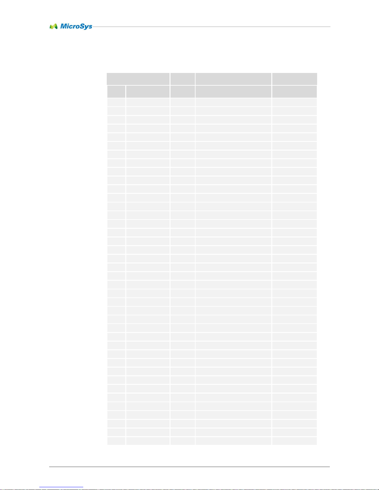
Peripherals 9
miriac SBC-S32V User Manual
V 1.1
67/81
© MicroSys Electronics GmbH 2017
9.4.3 MIPIB Connector
MIPIB
IO
Description
S32V234
Pin
Signal
Voltage Port
1
+5.0V Supply
2 n.c.
3 +5.0V Supply
4 n.c.
5 GND
Reference Ground
6 GND
Reference Ground
7
CSI1-CLK
1.0V
27MHz Clock
8
CSI1-DT2+
1.0V
MIPI Lane 2
9 GND
Reference Ground
10
CSI1-DT2-
1.0V
MIPI Lane 2
11
CSI1-SDA
1.8V
I²C Bus 1
PG5
12
GND
Reference Ground
13
CSI1-SCL
1.8V
I²C Bus 1
PG6
14
CSI1-DT0+
1.0V
MIPI Lane 0
15
n.c.
16
CSI1-DT0-
1.0V
MIPI Lane 0
17
n.c.
18
GND
Reference Ground
19
n.c.
20
CSI1-CLK+
1.0V
MIPI Clock
21
CSI1-RST#
1.8V
Reset Line
PB15
22
CSI1-CLK-
1.0V
MIPI Clock
23
GND
Reference Ground
24
GND
Reference Ground
25
+5V/+12V
Supply via PWB
26
CSI1-DT1+
1.0V
MIPI Lane 1
27
+5V/+12V
Supply via PWB
28
CSI1-DT1-
1.0V
MIPI Lane 1
29
GND
Reference Ground
30
GND
Reference Ground
31
n.c.
32
CSI1-DT3+
1.0V
MIPI Lane 3
33
n.c.
34
CSI1-DT3-
1.0V
MIPI Lane 3
35
CSI1-SYN
1.8V
Sync Line
PB11
36
n.c.
37
FXT1-CH0
1.8V
t.b.d.
PC9
38
n.c.
39
FXT1-CH1
1.8V
t.b.d.
PC10
40
n.c.
Page 68

Peripherals 9
miriac SBC-S32V User Manual
V 1.1
68/81
© MicroSys Electronics GmbH 2017
9.5 MicroSD Card Slot
The SBC-S32V system offers two microSD Card interfaces. The microSD card A
can also be configured as a boot device. Both SD cards work with 3.3V operation
voltage. SD card slot B is a mounting option and not installed in the standard
version.
Manufacturer:
Yamaichi
Type:
PJS-008-2130-0
Used with:
microSD cards
microSD card slot A interconnection:
I/O
Range
SDHCA S32V234
Pin
Name
Pin
Signal
Port
LVTTL 1 DAT2
↔
V21
SD_DAT2
PK10
LVTTL 2 CD/DAT3
↔
V22
SD_DAT3
PK11
LVTTL 3 CMD
←
U22
SD_CMD
PK7
4 Vdd
LVTTL 5 CLK
←
V25
SD_CLK
PK6
6 Vss
LVTTL 7 DAT0
↔
V23
SD_DAT0
PK8
LVTTL 8 DAT1
↔
U23
SD_DAT1
PK9
LVTTL 9 SW1
→
U25
SD_WP
PK5
Table 11 microSD card slot pin assignment
Figure 38: micro SD-Card A
Page 69

Peripherals 9
miriac SBC-S32V User Manual
V 1.1
69/81
© MicroSys Electronics GmbH 2017
microSD card slot B interconnection:
I/O
Range
SDHCA S32V234
Pin
Name
Pin
Signal
Port
LVTTL 1 DAT2
↔
N20
SD_DAT2
PF5
LVTTL
2
CD/DAT3
↔
N25
SD_DAT3
PF6
LVTTL 3 CMD
←
P22
SD_CMD
PF2
4 Vdd
LVTTL 5 CLK
←
P21
SD_CLK
PF1
6 Vss
LVTTL 7 DAT0
↔
M20
SD_DAT0
PF3
LVTTL 8 DAT1
↔
N23
SD_DAT1
PF4
LVTTL 9 SW1
→
P23
SD_WP
PF0
Table 12 microSD card slot pin assignment
Figure 39: not fitted SDHC-B connector
Page 70
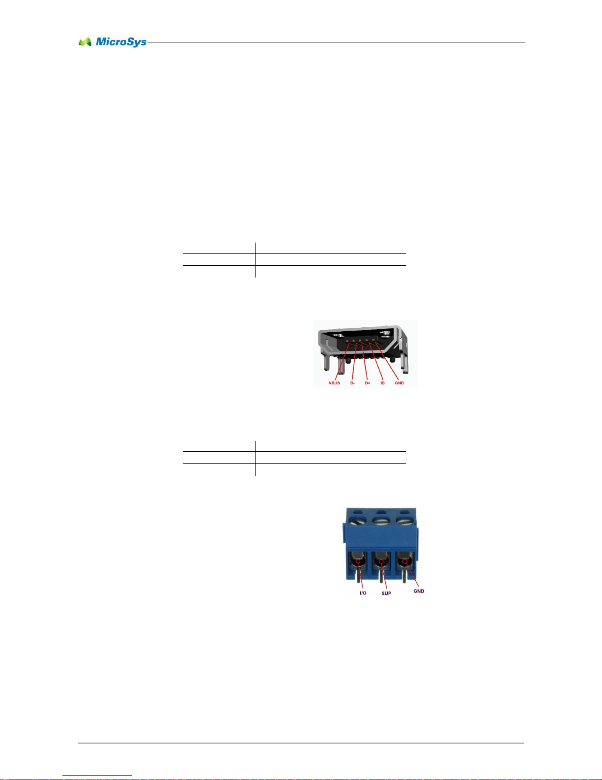
Peripherals 9
miriac SBC-S32V User Manual
V 1.1
70/81
© MicroSys Electronics GmbH 2017
9.6 UART
The SBC-S32V system is provided with two serial UART interfaces.
UART1 is converted to USB 2.0 for easy console port connection with a PC.
UART2 is converted to the LIN 2.1 standard and available on a three-terminal wire
connector.
9.6.1 UART1
Manufacturer:
Würth Elektronik
Type:
629 105 150 521
Mates with:
Standard Micro USB plug
9.6.2 UART2
Manufacturer:
Würth Elektronik
Type:
691 214 110 003
Mates with:
0.2-1.5mm² wire
Figure 40 micro USB
Figure 41 LIN Connector
Page 71

Peripherals 9
miriac SBC-S32V User Manual
V 1.1
71/81
© MicroSys Electronics GmbH 2017
9.7 CAN
The SBC-S32V system offers two CAN-FD interfaces. CAN0 and CAN1 are
accessible via two 2-terminal wire connectors. The necessary 120 ohms end-point
termination can be activated by two dip switches
9.7.1 CAN0
Manufacturer:
Würth Elektronik
Type:
691 214 110 002
Mates with:
0.2-1.5mm² wire
9.7.2 CAN1
Manufacturer:
Würth Elektronik
Type:
691 214 110 002
Mates with:
0.2-1.5mm² wire
Figure 42: CAN0 Terminal Block
Figure 43:CAN1 Terminal Block
Page 72

Peripherals 9
miriac SBC-S32V User Manual
V 1.1
72/81
© MicroSys Electronics GmbH 2017
9.7.3 Termination
The termination is located in the middle behind the terminal blocks. It is activated if
the according dip switch is set to ON.
Manufacturer:
Würth Elektronik
Type:
416131160802
Setting
TERM-1
TERM-2
CAN0
CAN1
OFF
OFF
no termination
no termination
ON
OFF
120R termination
no termination
OFF
ON
no termination
120R termination
ON
ON
120R termination
120R termination
Figure 44: CAN Termination Switch
Page 73

Peripherals 9
miriac SBC-S32V User Manual
V 1.1
73/81
© MicroSys Electronics GmbH 2017
9.8 LEDs
The CRX-S32V carrier contains 5 LEDs. There is one power led, two user LEDs
and two ethernet traffic indicators. The green power led located underneath the
power switch indicates the supply of +12V. The yellow user led, located under the
HDMI connector, is connected to the CPU port PA8 and the red user led directly
under the LAN jack uses CPU port PA9. The ethernet LEDs are integrated into the
RJ45 jack and indicate link status and traffic.
Led
Color
ON
OFF
Description
LD1
green
Power Switch On
Power Switch Off
+12V applied
LD2
yellow
CPU-PA8=high
CPU-PA8=low
Uses FLXR-TXD signal
LD3
red
CPU-PA9=high
CPU-PA9=low
Uses FLXR-RXD signal
LAN-B
yellow
Receive / Transmit
no traffic
KSZ9031 LED1 Control
LAN-C
yellow
Link active
no link
KSZ9031 LED2 Control
Figure 45: Carrier LEDs
Page 74

Peripherals 9
miriac SBC-S32V User Manual
V 1.1
74/81
© MicroSys Electronics GmbH 2017
9.9 Switches
The SBC-S32V contains five switches, three of them are located on the carrier and
two on the module. The main power switch PWR, the boot mode switches BOOT
and BMD, the CAN termination switch TERM and the GPU power enable switch.
The power switch is an alternate action pushbutton switch to enable or disable
power on all power rails for the whole system. For more information refer to 4.15.3
Input Power Switch.
The boot mode switch is used to select between 4 possible boot configurations,
implemented in the MCU. For more information refer to 5.3 Boot Mode Switch and
5.2 Power Up Configuration
Page 75

Peripherals 9
miriac SBC-S32V User Manual
V 1.1
75/81
© MicroSys Electronics GmbH 2017
The CAN termination switch is used to enable or disable a 120R termination
resistor for each CAN line. For more information refer to 9.7.3 Termination
The GPU power enable switch is used to reduce power consumption, in case the
GPU is not used. For more information refer to chapter 6.5 Switches
Page 76

Peripherals 9
miriac SBC-S32V User Manual
V 1.1
76/81
© MicroSys Electronics GmbH 2017
9.10 Jumpers
There are three jumper blocks onboard the SBC-S32V.
Two 5 pin headers for MIPI power selection
Anyway, only a single link per header must be set at a
time. More than one link installed may cause permanent
damage to the board!
One 2 pin header for the JTAG configuration
Figure 46: MIPI-A Power Selection
Figure 48: JRS Link
Figure 47: MIPI-B Power Selection
Page 77

Appendix 10
miriac SBC-S32V User Manual
V 1.1
77/81
© MicroSys Electronics GmbH 2017
10 Appendix
10.1 Acronyms
These acronyms are being used within the document; note that this list does not
claim to be complete or exhaustive:
ADAS ........................................................................Advanced Driver Assistance Systems
ARM ............................................................................................ Advanced RISC Machine
BaseT .................................................................... Ethernet over twisted pair technologies
BIST .......................................................................................................... Built In Self-Test
CAN-FD ...................................................... Controller Area Network with flexible Data rate
CEC ..................................................................................... Consumer Electronics Control
Cortex-M4 ...................................................................................... ARMv7E-M architecture
CPU ............................................................................................... Central Processing Unit
CR2032 ......................................................................................... IEC standard button cell
CSI ................................................................................................ Camera Serial Interface
DDC .................................................................................................. Display Data Channel
eMMC ...................................................................................... embedded Multimedia Card
ESD ................................................................................................ Electrostatic Discharge
FR4 ........................................................................................................... flame retardant 4
GND ........................................................................................................................ Ground
GPIO ................................................................................................... General Purpose IO
GPL ................................................................................................ General Public License
GPU .............................................................................................. Graphic Processing Unit
HDMI .......................................................................... High-Definition Multimedia Interface
I²C .................................................................................................... Inter-Integrated Circuit
JTAG .............................................................................................. Joint Test Action Group
Kinetis ............................................................................................ ARM® Cortex-M0+ core
LAN ...................................................................................................... Local Area Network
LED ..................................................................................................... Light Emitting Diode
LIN ............................................................................................ Local Interconnect Network
MCU ..................................................................................................... Microcontroller Unit
MIPI ........................................................................... Mobile Industry Processor Interface
MPX ............................................................................................... MicroSys miriac Module
MXM ........................................................................................ Mobile PCI Express Module
POL ............................................................................................................. Point Of Load
PPTC ............................................................. Polymeric Positive Temperature Coefficient
RCON .................................................................................................. Reset Configuration
RJ45 ..................................................................................................... Registered Jack 45
RTC ........................................................................................................... Real Time Clock
SBC ................................................................................................ Single Board Computer
SOM ......................................................................................................System On Module
TFTP ...................................................................................... Trivial File Transfer Protocol
TVS ...................................................................................... Transient Voltage Suppressor
UART .......................................................... Universal Asynchronous Receiver Transmitter
U-Boot ...................................................................................... The Universal Boot Loader
USB ..................................................................................................... Universal Serial Bus
Page 78

Appendix 10
miriac SBC-S32V User Manual
V 1.1
78/81
© MicroSys Electronics GmbH 2017
10.2 Table of Figures
Figure 1 Boot Switch ............................................................................................................ 10
Figure 2: BMD Switch .......................................................................................................... 10
Figure 3: GPU Switch ........................................................................................................... 10
Figure 4 USB Connector ...................................................................................................... 10
Figure 5 Power Switch Off.................................................................................................... 11
Figure 6 Power Jack ............................................................................................................ 11
Figure 7 Power Switch ON ................................................................................................... 11
Figure 8 Mechanical Dimensions ......................................................................................... 17
Figure 9: Module Side connectors (carrier CRX-S32V) ........................................................ 19
Figure 10 Non-Module Side connectors (carrier CRX-S32V) ............................................... 20
Figure 11:PN12SHSA03QE ................................................................................................. 27
Figure 12: G003-Series ........................................................................................................ 27
Figure 13 Power supply structure ......................................................................................... 28
Figure 14: Connector PWE1 & PWE2 .................................................................................. 29
Figure 15: Header PWA & PWB ........................................................................................... 30
Figure 16: BMD Switch ........................................................................................................ 34
Figure 17: Position BTM0=low ............................................................................................. 34
Figure 18: Position BTM1=low ............................................................................................. 34
Figure 19: Boot Mode Switch ............................................................................................... 35
Figure 20: Module MCU Connector ...................................................................................... 37
Figure 21: Carrier MCU Connector ...................................................................................... 38
Figure 22: MPX-Leds ........................................................................................................... 45
Figure 23: GPU switch ......................................................................................................... 46
Figure 24: GPU Power Off ................................................................................................... 46
Figure 25: GPU Power On ................................................................................................... 46
Figure 26: BMD Switch ........................................................................................................ 46
Figure 27: MXM-Connector .................................................................................................. 47
Figure 28: JTAG Connector ................................................................................................ 55
Figure 29: TRST Connect .................................................................................................... 55
Figure 30: Battery Holder & Battery ..................................................................................... 58
Figure 31: HDMI Type A ...................................................................................................... 60
Figure 32: LAN-Jack ............................................................................................................ 61
Figure 33: miniPCIe Slot ...................................................................................................... 62
Figure 34: mini PCIe Slot ..................................................................................................... 62
Figure 35:Power Conector PWE1 ........................................................................................ 62
Figure 36: mini PCI-E 4H Type I G/F ................................................................................... 63
Figure 37: MIPI Configuration .............................................................................................. 64
Figure 38: micro SD-Card A ................................................................................................. 68
Figure 39: not fitted SDHC-B connector ............................................................................... 69
Figure 40 micro USB ............................................................................................................ 70
Figure 41 LIN Connector ...................................................................................................... 70
Figure 42: CAN0 Terminal Block .......................................................................................... 71
Figure 43:CAN1 Terminal Block ........................................................................................... 71
Figure 44: CAN Termination Switch ..................................................................................... 72
Page 79

Appendix 10
miriac SBC-S32V User Manual
V 1.1
79/81
© MicroSys Electronics GmbH 2017
Figure 45: Carrier Leds ........................................................................................................ 73
Figure 46: MIPI-A Power Selection ...................................................................................... 76
Figure 47: MIPI-B Power Selection ...................................................................................... 76
Figure 48: JRS Link .............................................................................................................. 76
Page 80

Appendix 10
miriac SBC-S32V User Manual
V 1.1
80/81
© MicroSys Electronics GmbH 2017
10.3 Table of Tables
Table 1 Symbols .................................................................................................................... 6
Table 2 Conventions .............................................................................................................. 6
Table 3 Safety and Handling Precautions .............................................................................. 7
Table 4: MXM Connector ..................................................................................................... 54
Table 5 JTAG Header .......................................................................................................... 55
Table 6 I²C0 bus map ........................................................................................................... 57
Table 7 I²C1 bus map ........................................................................................................... 57
Table 8 I²C2 bus map ........................................................................................................... 57
Table 9 DDC Function .......................................................................................................... 59
Table 10 miniPCIe Slot pinout .............................................................................................. 63
Table 11 microSD card slot pin assignment ......................................................................... 68
Table 12 microSD card slot pin assignment ......................................................................... 69
Table 13 Document history .................................................................................................. 81
Page 81

History 11
miriac SBC-S32V User Manual
V 1.1
81/81
© MicroSys Electronics GmbH 2017
11 History
Date
Version
Change Description
2017-07-26
1.0
Initial Release Version (preliminary)
2017-08-01
1.01
MIPI Chapter and Rev, 2 photos added
2017-09-01
1.1
Some review inputs implemented. Typos corrected.
Default setting for switches marked.
Preliminary watermark removed.
Table 13 Document history
Page 82

Mouser Electronics
Authorized Distributor
Click to View Pricing, Inventory, Delivery & Lifecycle Information:
NXP:
SBC-S32V234
 Loading...