

MicroSys miriac SBC-T1024, miriac SBC-LS1088A, miriac SBC-T104, miriac SBC-LS1046A User Manual
miriac SBC-T1024
User Manual (CRX05 Revision 2 + Revision 3)
V 2.3

Table of Contents
miriac SBC-T1024 User Manual
V 2.3
2/70
© MicroSys Electronics GmbH 2017
Table of Contents
1 General Notes .............................................. 4
1.1 Warranty ........................................................ 4
1.2 Links .............................................................. 4
1.3 Liability .......................................................... 4
1.4 Offer to Provide Source Code of Certain
Software ........................................................ 5
1.5 Symbols, Conventions and Abbreviations ..... 6
1.5.1 Symbols ........................................................ 6
1.5.2 Conventions .................................................. 6
2 Introduction ................................................. 7
2.1 Safety and Handling Precautions .................. 7
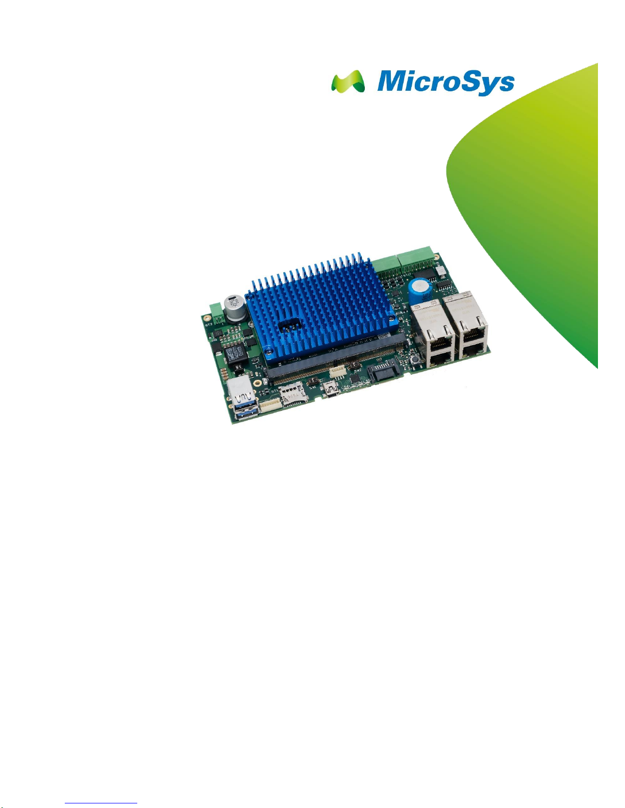
2.2 Short Description ........................................... 8
2.3 Shipping List .................................................. 8
2.4 Feature Changelist for HW Revisions ........... 8
2.4.1 Changes from revision 2 to revision 3 ........... 8
2.4.2 Feature Changelist for HW Revision 2 .......... 9
2.5 Functional Coverage ................................... 10
3 Quick Start Guide ...................................... 11
3.1 Prerequisites ............................................... 11
3.1.1 Minimum Requirements .............................. 11
3.1.2 Recommended Items .................................. 11
3.2 Board Preparation and Power-Up ............... 12
3.3 Operation .................................................... 13
3.3.1 U-Boot Startup............................................. 13
3.3.2 Linux ............................................................ 14
4 System Description ................................... 15
4.1 Block Diagram ............................................. 15
4.2 Feature Overview ........................................ 15
4.3 Mechanical Dimensions .............................. 17
4.3.1 MPX-T1024 ................................................. 17
4.3.2 SBC-T1024 ................................................. 18
4.4 Connector Layout – Top .............................. 19
4.5 Connector Layout – Bottom ......................... 20
4.6 Power Supply .............................................. 21
4.6.1 Input Supply Rating ..................................... 21
4.6.2 Input Power Connector ................................ 21
4.6.3 Power Supply Structure ............................... 21
4.6.4 RTC Backup Battery .................................... 22
4.6.5 Current Measurement ................................. 23
4.6.6 Fuses .......................................................... 23
5 System Core, Boot Configuration and
On-Board Memory ..................................... 24
5.1 Processor NXP T1024 ................................. 24
5.2 JTAG Chain ................................................. 24
5.3 Reset Structure ........................................... 24
5.4 Clock Distribution ......................................... 26
5.5 Boot Configuration ....................................... 28
5.6 NAND Flash ................................................. 29
5.7 SPI Flash ..................................................... 30
5.8 I²C Bus......................................................... 31
5.8.1 I2C-1 ............................................................ 31
5.8.2 I2C-2 ............................................................ 32
6 Peripherals ................................................. 34
6.1 Connector References ................................. 34
6.2 Module Connector ....................................... 35
6.3 LAN Connections ......................................... 35
6.3.1 Port 1 / 2 / 3 ................................................. 36
6.3.2 Port 4 ........................................................... 36
6.4 PCIe Connections ........................................ 38
6.4.1 Mini-PCIe Slot .............................................. 38
6.4.2 Mini-PCIe Slot / mSATA Slot ....................... 40
6.4.3 PCIe Extension Connector 1 ....................... 42
6.4.4 PCIe Extension Connector 2 ....................... 43
6.4.5 PCIe with external clock .............................. 44
6.5 SATA ........................................................... 45
6.6 MicroSD Card Slot ....................................... 46
6.7 USB ............................................................. 47
6.7.1 USB1 ........................................................... 47
6.7.2 USB2 ........................................................... 48
6.7.3 USB3 ........................................................... 49
6.8 UART ........................................................... 50
6.9 MCU Connector ........................................... 51
6.10 JTAG Connector .......................................... 52
6.10.1 JTAG on Revision R3 .................................. 52
6.10.2 JTAG on Revision R2 .................................. 53
6.11 Aurora Connectors (optional) ....................... 54
6.12 General Purpose Inputs / Outputs ............... 55
6.13 Fan Connector ............................................. 57
6.14 Smart Card Connector ................................. 58
6.15 emBRICK Connector ................................... 59
7 Switches, Buttons and Jumpers .............. 60
7.1 Boot Device Switch ...................................... 60
7.2 Board Configuration Switch ......................... 61
7.3 PCIe selection: root complex / endpoint ...... 61
7.4 Reset Button ................................................ 62
8 LEDs ........................................................... 63
8.1 RJ45 LEDs .................................................. 63
8.2 Power And Reset LEDs ............................... 64
8.3 RGB LEDs ................................................... 65

Table of Contents
miriac SBC-T1024 User Manual
V 2.3
3/70
© MicroSys Electronics GmbH 2017
9 Software ..................................................... 66
9.1 U-Boot ......................................................... 66
9.2 Operating System Support .......................... 66
9.3 Flash Layout ................................................ 66
9.3.1 NAND Flash ................................................ 66
9.3.2 SD Card ...................................................... 66
9.3.3 SPI Flash ..................................................... 66
10 Appendix .................................................... 67
10.1 Acronyms ..................................................... 67
10.2 Table of Figures ........................................... 68
10.3 Table of Tables ............................................ 68
11 History ........................................................ 70

General Notes 1
miriac SBC-T1024 User Manual
V 2.3
4/70
© MicroSys Electronics GmbH 2017
1 General Notes
Copyright MicroSys Electronics GmbH, January 2017
All rights reserved. All rights in any information which appears in this document
belong to MicroSys Electronics GmbH or our licensors. You may copy the
information in this manual for your personal, non-commercial use.
Copyrighted products are not explicitly indicated in this manual. The absence of the
copyright (©) and trademark (TM or ®) symbols does not imply that a product is not
protected. Additionally, registered patents and trademarks are similarly not
expressly indicated in this manual.
1.1 Warranty
To the extent permissible by applicable law all information in this document is
provided without warranty of any kind, whether expressed or implied, including but
not limited to any implied warranty of satisfactory quality or fitness for a particular
purpose, or of non-infringement of any third party’s rights. We try to keep this
document accurate and up-to-date but we do not make any warranty or
representation about such matters. In particular we assume no liability or
responsibility for any errors or omissions in this document.
MicroSys Electronics GmbH neither gives any guarantee nor accepts any liability
whatsoever for consequential damages resulting from the use of this manual or its
associated product.
MicroSys Electronics GmbH further reserves the right to alter the layout and/or
design of the hardware without prior notification and accepts no liability for doing
so.
1.2 Links
We make no warranty about any other sites that are linked to or from this
document, whether we authorise such links or not.
1.3 Liability
To the extent permissible by applicable law, in no circumstance, including (but not
limited to) negligence, shall we be liable for your reliance on any information in this
document, nor shall we be liable for any direct, incidental, special, consequential,
indirect or punitive damages nor any loss of profit that result from the use of, or the
inability to use, this document or any material on any site linked to this document
even if we have been advised of the possibility of such damage. In no event shall
our liability to you for all damages, losses and causes of action whatsoever,
whether in contract, tort (including but not limited to negligence) or otherwise
exceed the amount, if any, paid by you to us for gaining access to this document.
MicroSys Electronics GmbH
Muehlweg 1
D-82054 Sauerlach
Germany
Phone: +49 8104 801-0
Fax: +49 8104 801-110

General Notes 1
miriac SBC-T1024 User Manual
V 2.3
5/70
© MicroSys Electronics GmbH 2017
1.4 Offer to Provide Source Code of Certain
Software
This product contains copyrighted software that is licensed under the General
Public License (“GPL”) and under the Lesser General Public License Version
(“LGPL”). The GPL and LGPL licensed code in this product is distributed without
any warranty. Copies of these licenses are included in this product.
You may obtain the complete corresponding source code (as defined in the GPL)
for the GPL Software, and/or the complete corresponding source code of the LGPL
Software (with the complete machine-readable “work that uses the Library”) for a
period of three years after our last shipment of the product including the GPL
Software and/or LGPL Software, which will be no earlier than December 1, 2010,
for the cost of reproduction and shipment, which is dependent on the preferred
carrier and the location where you want to have it shipped to, by sending a request
to:
MicroSys Electronics GmbH
Muehlweg 1
D-82054 Sauerlach
Germany
In your request please provide the product name and version for which you wish to
obtain the corresponding source code and your contact details so that we can
coordinate the terms and cost of shipment with you.
The source code will be distributed WITHOUT ANY WARRANTY and licensed
under the same license as the corresponding binary/object code.
This offer is valid to anyone in receipt of this information.
MicroSys Electronics GmbH is eager to duly provide complete source code as
required under various Free Open Source Software licenses. If however you
encounter any problems in obtaining the full corresponding source code we would
be much obliged if you give us a notification to the email address
gpl@microsys.de, stating the product and describing the problem (please do NOT
send large attachments such as source code archives etc to this email address)
General Notes 1
miriac SBC-T1024 User Manual
V 2.3
6/70
© MicroSys Electronics GmbH 2017
1.5 Symbols, Conventions and Abbreviations
1.5.1 Symbols
Throughout this document, the following symbols will be used:
Information marked with this symbol MUST be
obeyed to avoid the risk of severe injury, health
danger, or major destruction of the unit and its
environment
Information marked with this symbol MUST be
obeyed to avoid the risk of possible injury,
permanent damage or malfunction of the unit.
Information marked with this symbol gives important
hints upon details of this manual, or in order to get
the best use out of the product and its features.
Table 1-1 Symbols
1.5.2 Conventions
Symbol
explanation
#
denotes a low active signal
←
denotes the signal flow in the shown direction
→
denotes the signal flow in the shown direction
↔
denotes the signal flow in both directions
→
denotes the signal flow in the shown direction with additional logic /
additional ICs in the signal path
I/O
denotes a bidirectional pin
Input
denotes an input pin
matched
denotes the according signal to be routed impedance controlled and
length matched
Output
denotes an output pin
Pin 1
refers to the numeric pin of a component package
Pin a1
refers to the array position of a pin within a component package
XXX-
denotes the negative signal of a differential pair
XXX+
denotes the positive signal of a differential pair
XXX
denotes an optional not mounted or fitted part
Table 1-2 Conventions

Introduction 2
miriac SBC-T1024 User Manual
V 2.3
7/70
© MicroSys Electronics GmbH 2017
2 Introduction
Thank you for choosing the MicroSys SBC-T1024 Single Board Computer system.
This manual should help you to get the best performance and details out all of its
features.
2.1 Safety and Handling Precautions
ALWAYS use the correct type and polarity of the power supply!
DO NOT exceed the rated maximum values for the power
supply! This may result in severe permanent damage to the
unit, as well as possible serious injury.
ALWAYS keep the unit dry, clean and free of foreign objects.
Otherwise, irreparable damage may occur.
Parts of the unit may become hot during operation. Take care
not to touch any parts of the circuitry during operation to avoid
burns, and operate the unit in a well-ventilated location.
Provide an appropriate cooling solution as required.
ALWAYS take care of ESD-safe handling!
Many pins on external connectors are directly connected to the
CPU or other ESD sensitive devices.
Make or break ANY connections ONLY while the unit is
switched OFF.
Otherwise, permanent damage to the unit may occur, which is
not covered by warranty.
There is no separate SHIELD connection.
All the metal sheaths of shielded connectors are connected to
GND.
Also, all mounting holes of the carrier board are connected to
GND.
The module’s mounting holes are not connected to GND
Take this into account when handling and mounting the unit.
Table 2-1 Safety and Handling Precautions

Introduction 2
miriac SBC-T1024 User Manual
V 2.3
8/70
© MicroSys Electronics GmbH 2017
2.2 Short Description
The SBC-T1024 is a small computer system consisting of
■ the MPX-T1024 module, based on NXP’s T1024 Multicore Communications
Processors
■ and the CRX05 carrier board.
It targets both
■ evaluation of the respective MPX-T1024 SOM
■ direct usage as an industrial computing solution
This document gives you an overview on the board's connectors and how to take the
first steps on the initial setup.
2.3 Shipping List
The SBC-T1024 EvalKit package contains the following items:
■ The SBC-T1024 system, mounted with cooling solution
■ Power Supply 12V DC stabilized / 2 A
■ Cable adapter for the power supply
■ USB cable type A – mini B
■ Micro-SD-Card with U-Boot and root file system
2.4 Feature Changelist for HW Revisions
2.4.1 Changes from revision 2 to revision 3
The revision 3 of the carrier board provides following changes:
■ Added SW4 to switch between root complex and endpoint
■ Added 2 header for GND interconnection (JP1, JP2)
■ Addes buffer to SPI-CLK
■ Added possibility to modify board to run with external PCIe-clock, requires
hardwaremodification (default assembled to use internal clock)
■ Type of “JTG-connector” changed to JST-BM14B-SRSS-TB

Introduction 2
miriac SBC-T1024 User Manual
V 2.3
9/70
© MicroSys Electronics GmbH 2017
2.4.2 Feature Changelist for HW Revision 2
The revision 2 of the carrier board provides new features:
■ Added LED driver with 4x RGB LEDs
■ Added 12 GPIOs (6x in / 6x out) addressable via I²C
o Output voltage level maximum 24V (according to the input voltage
of the carrier board)
o Input voltage range 24V maximum
■ Added SuperCap for RTC backup battery (CR2032 coin cell as assembly
option still available)
■ Added prerequisites for support of emBRICK devices
■ Added current shunt for current measurements
■ Added optional (by assembly option) support for onboard current
measurements of the CPU module consumption via I²C current sense
amplifier
■ Added LAN interrupt support
■ Added SMART CARD connector
■ Added optional (by assembly option) extension connector (for example for
additional GPIOs or graphic support if provided by the CPU)
■ Added mounting holes for the carrierboard
■ Added a fan connector
■ Added connector labeling (silkscreen) on the PCB
Some features were changed:
■ SerDes 6 and SerDes 7 lanes were swapped in order to achieve a wider
functional coverage within the MPX2 module family
o SerDes 6 is now connected to the SATA connector (ST10)
o SerDes 7 is now connected to the mPCIe / mSATA slot (ST7)
■ Improved power input section with filters
■ Improved mechanical mounting of the CPU module and mPCIe/ mSATA
cards
■ Replaced PCIe x1 edge card connector with second PCIe extension
connector
Introduction 2
miriac SBC-T1024 User Manual
V 2.3
10/70
© MicroSys Electronics GmbH 2017
2.5 Functional Coverage
The following table shows the coverage achieved by the SBC-T1024 compared to
the features which are available on the carrierboard:
Interfaces provided by CRX05 carrierboard
Interfaces available with the SBC-
T1024
SerDes 0
PCIe
-
SerDes 1
SGMII
-
SerDes 2
SGMII
-
SerDes 3
SGMII
-
SerDes 4
mPCIe / Aurora
✓ (mPCIe)
SerDes 5
PCIe
✓
SerDes 6
SATA
-
SerDes 7
mPCIe / mSATA
✓ (mSATA)
RGMII 1
PHY
✓
USB 1
2.0 / 3.0
✓ (2.0)
USB 2
2.0 / 3.0
✓ (2.0)
SD-Card
1bit / 4 bit & boot device
✓
UART 1
UART to USB
(debug console)
✓
UART 2
TTL only
✓
I²C 1
Multiple devices
✓
I²C 2
Multiple devices
✓
JTAG
Signals on non-standard
connector
✓
Watchdog
Hardware watchdog with
trigger signal from module
✓
RTC backup
Supercap
✓
Manual Reset
Button
✓
Reset LEDs
2x red
✓
Power LED
1x green
✓
Table 2-2 Functional coverage

Quick Start Guide 3
miriac SBC-T1024 User Manual
V 2.3
11/70
© MicroSys Electronics GmbH 2017
3 Quick Start Guide
3.1 Prerequisites
Always make sure to handle the SBC-T1024 unit ESD-safe!
Otherwise, the unit may suffer permanent damage.
However, do not place the unit directly flat on a metal surface,
as this may result in short circuits and damage to the board.
At first time operation unpack the unit and make sure that is clean and free of visible
damage or foreign objects.
3.1.1 Minimum Requirements
To operate the board, you will at least need the following items:
■ an adequate power supply, delivering 12V DC (stabilized) / 2A minimum.
■ an USB cable (type A – mini B) adapted to connector ST5
■ a serial terminal, such as a PC with an USB port running a terminal Software
(e.g. TeraTerm, HyperTerminal, putty, ckermit...), or else a hardware serial
console. Choose the following parameters:
(a) 115200 Bd
(b) 8 Data bits
(c) No parity
(d) 1 Stop Bit
3.1.2 Recommended Items
The following items are not absolutely necessary, but strongly recommended for
practical operation and development purposes:
■ Network connection via Port4 to your local network installation
■ TFTP server available for downloading within the network (Hint: may run on the
same PC as the serial Terminal)
■ SATA HDD/SSD and/or SD card as mass storage and/or boot media
Quick Start Guide 3
miriac SBC-T1024 User Manual
V 2.3
12/70
© MicroSys Electronics GmbH 2017
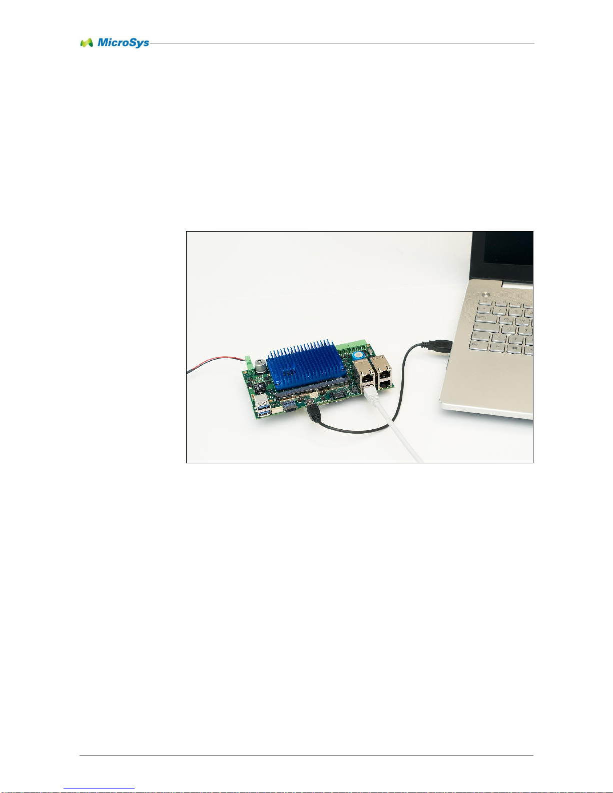
3.2 Board Preparation and Power-Up
■ Make sure the switches SW1 and SW2 are set properly in order to select the
correct boot source and board configuration
■ The board comes preconfigured to boot correctly on arrival.
■ Connect the mini USB cable to ST5.
■ Connect other peripherals (USB, LAN, SATA, ...) as far as intended.
■ Connect the power line to the ST3 connector, while the power supply is still
switched off.
■ Switch on the power.
Figure 3-1 System setup example (LAN port 4)
Quick Start Guide 3
miriac SBC-T1024 User Manual
V 2.3
13/70
© MicroSys Electronics GmbH 2017
3.3 Operation
After Power-up, the green LED on the module should light up
and any red LED should be off.
IF NOT, DISCONNECT THE UNIT FROM POWER AND CHECK
FOR FAULTS!
3.3.1 U-Boot Startup
When power is supplied the system will start.
On startup, U-Boot will come up similar to the following:
The exact output may vary, depending on U-Boot and MPX-T1024 module versions in
use.
U-Boot 2016.09 (Oct 20 2016 - 15:19:01 +0200)
CPU0: T1024, Version: 1.0, (0x85400010)
Core: e5500, Version: 2.1, (0x80241021)
Clock Configuration:
CPU0:1400 MHz, CPU1:1400 MHz,
CCB:400 MHz,
DDR:800 MHz (1600 MT/s data rate) (Asynchronous),
IFC:100 MHz
FMAN1: 700 MHz
QMAN: 400 MHz
L1: D-cache 32 KiB enabled
I-cache 32 KiB enabled
Reset Configuration Word (RCW):
00000000: 0810000e 00000000 00000000 00000000
00000010: 2d000001 00000002 68040000 21002000
00000020: 00000000 00000000 00000000 00036700
00000030: 00000000 076e0a00 00000000 00000006
Board: MPXT1024
I2C: ready
SPI: ready
DRAM: Detected UDIMM Fixed DDR4 on board
2 GiB (DDR4, 64-bit, CL=12, ECC on)
L2: 256 KiB enabled
Corenet Platform Cache: 256 KiB enabled
Using SERDES1 Protocol: 90 (0x5a)
NAND: 512 MiB
MMC: FSL_SDHC: 0
*** Warning - bad CRC, using default environment
Quick Start Guide 3
miriac SBC-T1024 User Manual
V 2.3
14/70
© MicroSys Electronics GmbH 2017
PCIe1: Root Complex, no link, regs @ 0xfe240000
PCIe1: Bus 00 - 00
PCIe2: disabled
PCIe3: Root Complex, no link, regs @ 0xfe260000
PCIe3: Bus 01 - 01
In: serial
Out: serial
Err: serial
USB: 100MHz SYSCLK
Net: Initializing Fman
MMC read: dev # 0, block # 2080, count 128 ...
Fman1: Uploading microcode version 107.4.2
FM1@DTSEC4 [PRIME]
Hit any key to stop autoboot: 0
=>
3.3.2 Linux
For detailed setup instructions, refer to the text document “linux-4.1.8-mpx1024.txt”
delivered in the "Linux" directory along with the unit!
The text document mentioned here may refer to an older version.
System Description 4
miriac SBC-T1024 User Manual
V 2.3
15/70
© MicroSys Electronics GmbH 2017
4 System Description
This section describes all parts of the SBC-T1024 system.
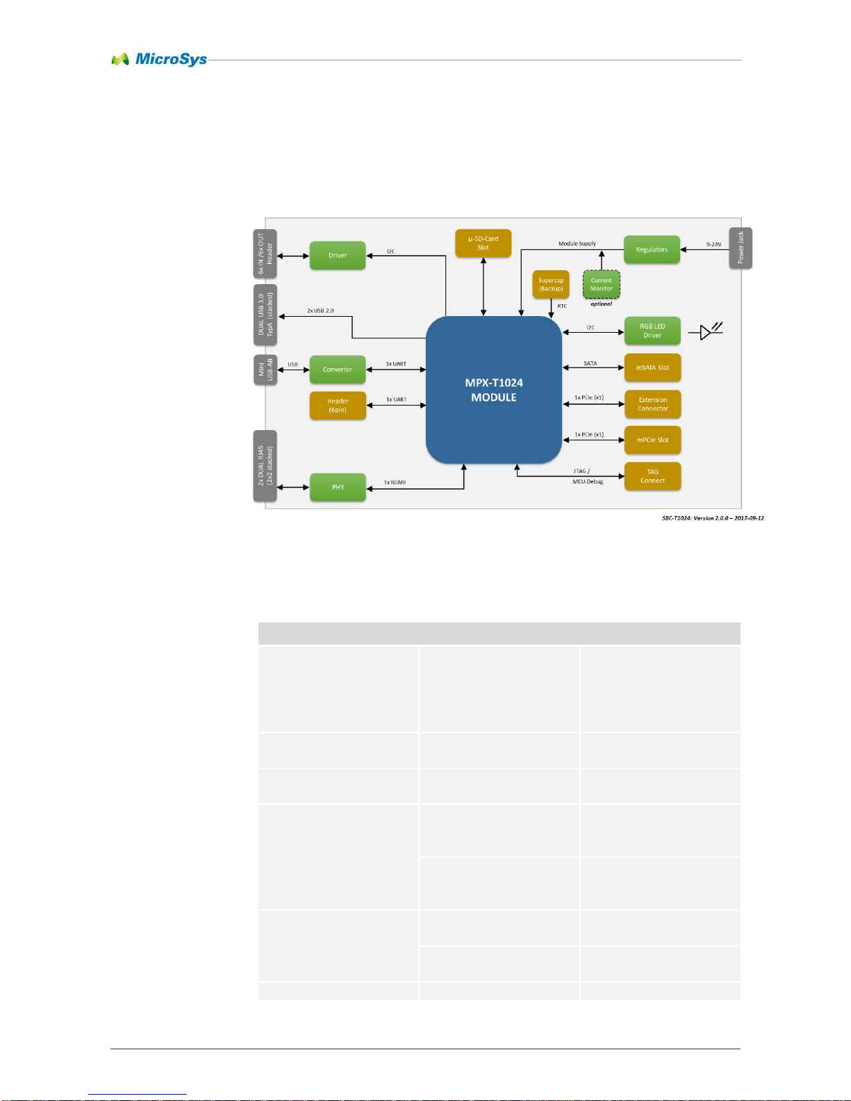
4.1 Block Diagram
4.2 Feature Overview
The SBC-T1024 offers the following features:
QorIQ e5500 cores 2xCPU Processor
SDRAM
64-bit DDR4 interface
Default: 2GByte
up to 8GByte
up to 1600MT/s
4 x DDR4 (x16)
single bank
Synchronous Memory
8-bit NAND Flash
Default: 512 MB
up to 2 GByte
Hard Disk Drives
Interface
SATA 2.0
mSATA slot
PCI Express port
2.0 / 5Gbps
Lane x1
Root complex operations
1x PCIe extension
connector
2.0 / 5Gbps
Lane x1
Root complex operations
1x Mini PCIe Slot
USB
USB 2.0 Phy
USB connector type A
USB 2.0 Phy
USB connector type A
Expansion Cards
MMC/SD/SDIO
micro SD card holder
Figure 4-1 Block Diagram (MPX-T1024 Revision 4 on carrier CRX05 Revision 2)
System Description 4
miriac SBC-T1024 User Manual
V 2.3
16/70
© MicroSys Electronics GmbH 2017
QorIQ e5500 cores 2xCPU Processor
Serial Interfaces
UART1
Converted to USB
(FT232),
Available on USB
connector type mini B
UART2
4-wire
Extension Port
LVTTL
I2C
I2C-1
400 kbps
Connected Devices:
LM95245
Temperature Sensor
AT24C128C
EEPROM
BR24G128NUX-3
EEPROM
RX-8803
RTC
IDT6V49205B
Clock Generator
TLC59116
RGB LED Driver
MAX7325
GPIO Port Expander
I2C-2
400 kbps
Connected Devices:
SC18IS602BIPW
I2C-to-SPI Bridge
MAX9611AUB
Current monitor
TCA9544APWR
I²C Multiplexer
Gigabit Ethernet
Controller
RGMII
10/100/1000 Mbps
System JTAG
Controller
JTAG
Different connector on
CRX05-R2 and R3
Power Management
Primary Supply
LM25116MH
Input:
9-30V DC
Output:
5V DC / peak 8A
Backup Supply
(RTC backup)
Supercap
Table 4-1 Feature Overview
System Description 4
miriac SBC-T1024 User Manual
V 2.3
17/70
© MicroSys Electronics GmbH 2017
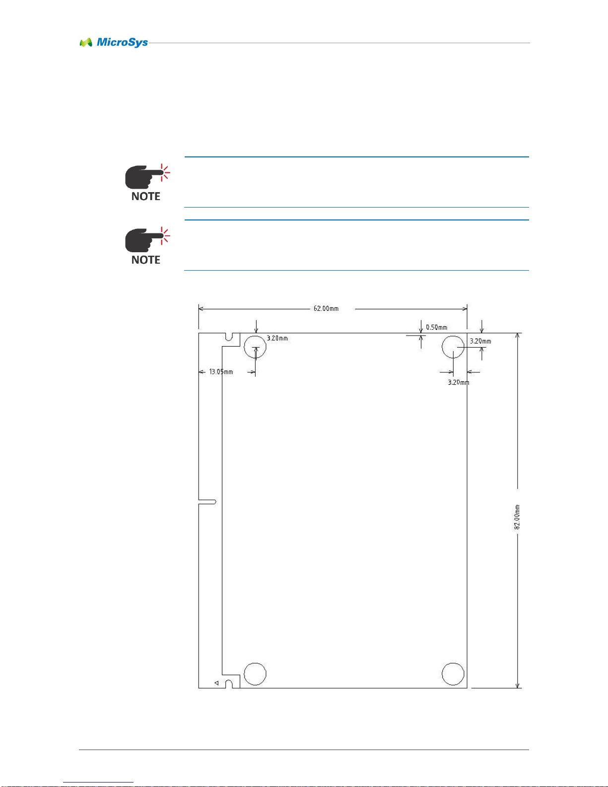
4.3 Mechanical Dimensions
4.3.1 MPX-T1024
The following drawing shows the mechanical outline of the MPX-T1024 module
that is plugged in the CRX05 carrier board.
This drawing is not to scale.
For 3D data files please contact MicroSys.
Figure 4-2 Mechanical Dimensions Modul
System Description 4
miriac SBC-T1024 User Manual
V 2.3
18/70
© MicroSys Electronics GmbH 2017
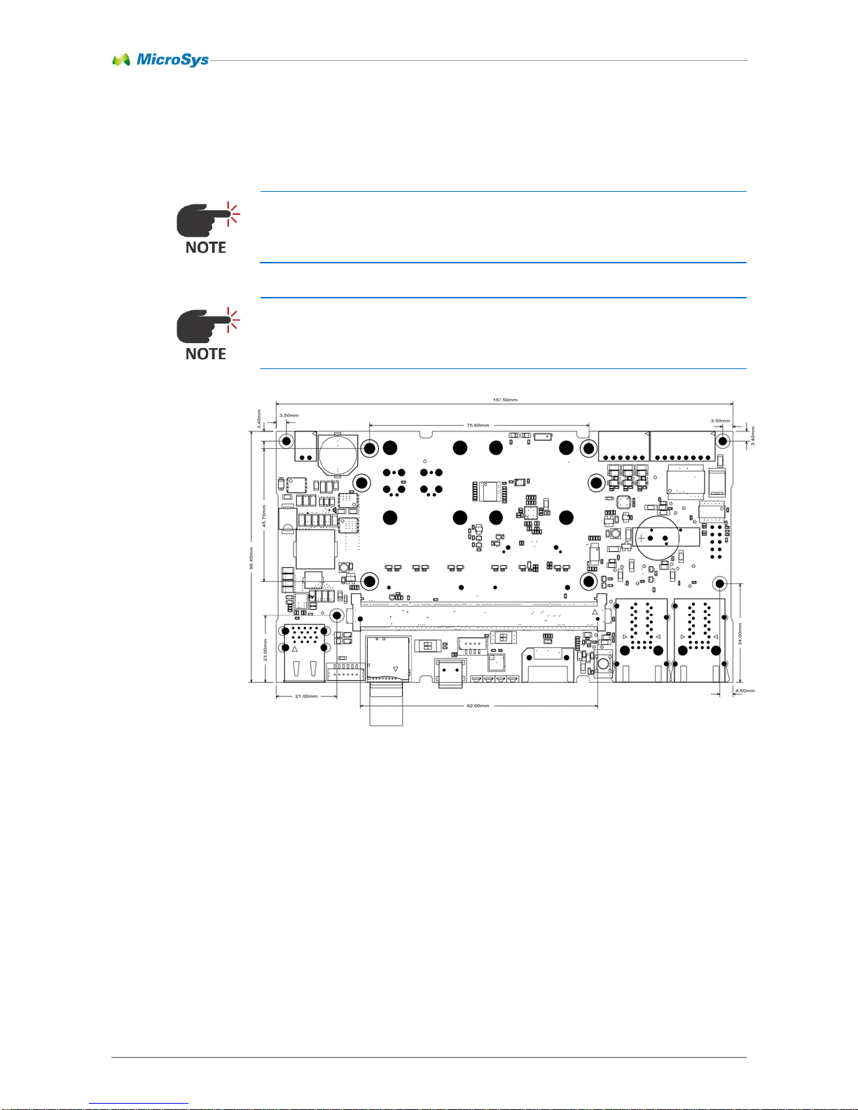
4.3.2 SBC-T1024
The following drawing shows the mechanical outline of the SBC-T1024 assembly.
This drawing is not to scale.
For 3D data files please contact MicroSys.
Figure 4-3 SBC-T1024 Mechanical Dimensions

System Description 4
miriac SBC-T1024 User Manual
V 2.3
19/70
© MicroSys Electronics GmbH 2017
4.4 Connector Layout – Top
Figure 4-4 Top connectors
System Description 4
miriac SBC-T1024 User Manual
V 2.3
20/70
© MicroSys Electronics GmbH 2017
4.5 Connector Layout – Bottom
Figure 4-5 Bottom connectors
System Description 4
miriac SBC-T1024 User Manual
V 2.3
21/70
© MicroSys Electronics GmbH 2017
4.6 Power Supply
4.6.1 Input Supply Rating
The SBC-T1024 system is run from a single DC power supply with the following
ratings:
Maximum Input Voltage Operating Range:
9V - 30V DC
Nominal Input Supply Voltage:
12V DC
Typical Current Consumption
(@12V / room temperature / U-boot prompt):
~0,6A
ALWAYS use the correct type and polarity of the power supply!
DO NOT exceed the rated maximum values for the power
supply! This may result in severe permanent damage to the
unit, as well as possible serious injury.
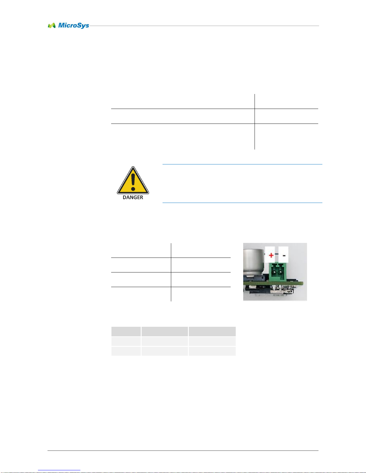
4.6.2 Input Power Connector
Part Reference
ST3
Manufacturer:
Würth Elektronik
Type:
691 382 010 002
Mates with:
691 381 000 002
(included in delivery)
Pin-out:
Pin
Name
Function
1
„+“
+VIN (= typ. 12V)
2
„-“
GND
Table 4-1 Pinout ST3
4.6.3 Power Supply Structure
■ Input Power from ST3 connector is fed to the primary step-down converter.
■ The primary step-down converter produces 5V DC / max. 8A peak from the
input supply which supplies both the T1024 module and peripheral devices on
the carrierboard CRX05.

System Description 4
miriac SBC-T1024 User Manual
V 2.3
22/70
© MicroSys Electronics GmbH 2017
■ The 5V DC are fed to a secondary step-down converter, which produces 3.3V
DC / max. 4A peak.
■ Two NCP1529 produce 1.8V and 1.5V from 3.3V, which are used for both
PCIe and onboard devices.
The following diagram shows the Power Supply structure:
4.6.4 RTC Backup Battery
The RTC on the module is supplied from a 470mF supercap that is loaded by the
5V power source on the carrier board.
Alternatively, there’s another version of the carrier board available that has a
backup battery holder for CR2032 batteries. Please contact MicroSys for more
information.
Part Reference:
BAT1
Manufacturer:
Renata Batteries
Type:
VBH2032-1
Used with:
CR2032 batteries
Figure 4-6 Power supply structure

System Description 4
miriac SBC-T1024 User Manual
V 2.3
23/70
© MicroSys Electronics GmbH 2017
4.6.5 Current Measurement
For current measurements the carrierboard provides a 10mΩ shunt resistor in the
5V path supplying the CPU module.
For automated measurements there’s a carrierboard version available that already
provides an I²C current sense amplifier.
The current sense amplifier is not populated by default.
For more information please contact MicroSys.
4.6.6 Fuses
There are no fuses on the SBC-T1024.

System Core, Boot Configuration and On-Board Memory 5
miriac SBC-T1024 User Manual
V 2.3
24/70
© MicroSys Electronics GmbH 2017
5 System Core, Boot Configuration
and On-Board Memory
5.1 Processor NXP T1024
The T1024 Processor by NXP is a QorIQ Power Architecture CPU with two CPU
cores. It exposes a wide variety of external interfaces, which are explained in detail
in the following chapters. Each core has a private 256KB L2 cache. Furthermore,
256KB shared L3 CoreNet platform cache is offered.
The two CPU cores run at a maximum clock speed of 1400 MHz, 1200 MHz or
1000 MHz respectively, depending on the ordered type. The CPU frequency can
be clocked down if necessary.
5.2 JTAG Chain
The JTAG chain of the SBC-T1024 includes the T1024 processor only. The JTAG
port is directly connected to the connector “JTG0”.
The JTAG connector footprint provides JTAG signals. For interfacing standard debugger pinouts an additional intermediate adapter is necessary.
Please see chapter Fehler! Verweisquelle konnte nicht gefunden werden. for a d
escription of the JTAG connector.
5.3 Reset Structure
Figure 5-1 Reset Structure (carrier CRX05 Revision 2)

System Core, Boot Configuration and On-Board Memory 5
miriac SBC-T1024 User Manual
V 2.3
25/70
© MicroSys Electronics GmbH 2017
Pin
Number
on ST4
Signal Name
Signal
Direction
Function
T136
RST-IN#
Input to the
module
Active low module reset:
while active the module is held in reset state
T135
RST-OUT#
Output from
the module
Active low peripheral reset:
while active peripheral devices shall be held in
reset state
B118
WDOG-TRIG#
Output from
the module
Watchdog service signal from the module
which has to be triggered periodically. When
the watchdog is active and the service stops
the module will be reset.
B111
MCU-HRST#
Bi-directional
Please contact MicroSys
B110
COP-PRST#
Input to the
module
Please contact MicroSys
B106
COP-TRST#
Input to the
module
Please contact MicroSys
Table 5-1 Reset signal overview
The default state for RST-IN# is active. Consequently the module is always in a reset
state when the RST-IN# signal is not actively driven high by the carrierboard.
The RST-IN# is an input to the module. It signals that the voltage supplies on the
carrierboard are within their limits and no manual reset is triggered. When active
(signal is low) the microcontroller unit on the module initiates the reset sequence in
order to keep the CPU in a defined reset state. No further interaction from the carrierboard is necessary. In case the module reset is active, the module triggers the
RST-OUT# signal which is intended to control the reset of peripheral devices on
the carrierboard i.e. Ethernet PHYs, PCIe slots and devices.
The RST-IN# signal can be triggered by either a powerfault situation, a manual reset button press (SW3) or a missing watchdog trigger signal WDOG-TRIG# from
the CPU in case the watchdog has been manually enabled beforehand via SW2.
MCU-HRST#, COP-PRST# and COP-TRST# are for JTAG and debugging purposes only.
The watchdog is off by default.
The watchdog is implemented on the carrier board.
The following voltages on the carrier board are monitored by a Maxim
MAX6751KA29 chip:
Voltage
Monitoring
Voltage Limit
3,3V
Undervoltage
Typ. 2,925V [2,867V-2,984V]
1,8V
Undervoltage
Typ. 1,72V [1,69V-1,75V]

System Core, Boot Configuration and On-Board Memory 5
miriac SBC-T1024 User Manual
V 2.3
26/70
© MicroSys Electronics GmbH 2017
Table 5-2 Voltage monitoring limits (carrier)
5.4 Clock Distribution
The following diagram shows the clock distribution of the SBC-T1024 system
T1024
ST4
ST1
Pin
Name
Signal
Pin
Signal
Pin
K1
SDHC_CL
K
→
10R
→
SDC-
CLK
B100 → →
→
SDC-CLK-
EMI
5
W1
IIC1_SCL
→ → →
I2C1-
SCL
B78 → → → See chapter 5.8.1
V3
IIC2_SCL
→ → →
I2C2-
SCL
B75 → → → See chapter 5.8.2
JTG0
E18
TCK
→ → →
JTCK
B105
→
10R → JTCK
6
J14
AF3
EC1_TX_
CLK
→
10R
→
MII1-
TXCK
T94 → → → TX_CLK
53
AD1
EC1_RX_
CLK
←
10R
←
MII1-
RXCK
T86 ← 10R ← RX_CLK
46
AG3
EC1_GTX
_CLK125
←
10R
←
MII1-
CRS
T83 ← ← ← CLK125
9
ST15
M4
DIU_CLK_
OUT
→
10R
→
DIUCLK
B54 → → → DIU-CLK
26
N1
SPI_CLK
→
10R
→
SPICLK
B69 → → → SPI-CLK
11
System Core, Boot Configuration and On-Board Memory 5
miriac SBC-T1024 User Manual
V 2.3
27/70
© MicroSys Electronics GmbH 2017
IDT6V49205B
T1024
Pin
Name
Name
Pin
23
PCIeT_LR0
→
SD-
REFCLK
1
AB14
24
PCIeC_LR0
→
SD-
REFCLK
1#
AA14
26
PCIeT_LR1
→
SPI-CLK
AB18
25
PCIeC_LR1
→
I2C1-
SCL
AA18
ST4
J6
Signal
Pin Signal
Pin
30
PCIeT_LR2
→
SRD-
CLK1+
T50 → SRC
19
29
PCIeC_LR2
→
SRD-
CLK1-
T51
→
SRC#
20
32
PCIeT_LR3
→
SRD-
CLK2+
T53
31
PCIeC_LR3
→
SRD-
CLK2-
T54
ST7
OUT0
2
→
PCIE-
CLKD+
13
OUT0#
3
→
PCIE-
CLKD-
11
ST8
OUT1
5
→
PCIE-
CLKB+
13
OUT1#
6
→
PCIE-
CLKB-
11
ST11
OUT2
12
→
PCIE-
CLKC+
A13
OUT2#
11
→
PCIE-
CLKC-
A14
ST9
OUT3
15
→
PCIE-
CLKA+
7
OUT3#
14
→
PCIE-
CLKA-
6
Table 5-3 Clock distribution and explanation

System Core, Boot Configuration and On-Board Memory 5
miriac SBC-T1024 User Manual
V 2.3
28/70
© MicroSys Electronics GmbH 2017
5.5 Boot Configuration
The SBC-T1024 board offers three possible boot devices to choose from. The settings can be done via SW1 (see chapter 7 for details).
SW1 configures two signals “BOOT-SEL1” and “BOOT-SEL2” which have a default
high state (10k pullups are on the module) when no connection is made or SW1 is
off. When the switch is on, the respective pin is grounded.
The BOOT-SELx pins are decoded to the following configuration (1= high, 0=low):
T1024
BOOT-SEL2 | BOOT-SEL1 =
Signal
Pin
SDHC
=[10]
SPI
=[11]
NAND
=[01]
IFC_AD08
B9 0 0
1
IFC_AD09
A9 0 0 0 IFC_AD10
A10 1 1 0 IFC_AD11
B11 0 0
0
IFC_AD12
A11 0 0 0 IFC_AD13
B12 0 0 0 IFC_AD14
A12 0 1 1 IFC_AD15
A13 0 0 1 IFC_CLE
F16 0 1
1
Table 5-4 Hard wired boot signals

System Core, Boot Configuration and On-Board Memory 5
miriac SBC-T1024 User Manual
V 2.3
29/70
© MicroSys Electronics GmbH 2017
5.6 NAND Flash
The SBC-T1024 system is equipped with 2GB of NAND Flash by default. Different
sizes may be available on request/order. The following table shows the
connections and signal levels for the NAND Flash.
I/O
Range
NAND Flash
SBC-
T1024
T1024
Description
Pin
Name
Signal
Pin
Name
1,8V
G5
LOCK Lock
1,8V
C8
RY/BY
→
NAND-
RB#
→
B15 /
A15
IFC_RB0# /
IFC_RB1#
ready/busy,
10K pullup
1,8V
D4
RE#
←
IFC-OE#
←
D15
IFC_OE#
read enable
1,8V
C6
CE#
←
NAND-
CS#
←
C13 /
E15
NANDF_CS0
chip select
1,8V
D3,G4,H8,
J6
VCC +1.8V
C5,F7,K3,
K8
GND GND
1,8V
D5
CLE
←
IFC-CLE
←
F16
IFC_CLE
command
latch enable
1,8V
C4
ALE
←
IFC-AVD
←
D17
IFC_AVD
address latch
enable
1,8V
C7
WE#
←
IFC-WE#
←
D13
IFC_WE0#
write enable
1,8V
C3
WP#
←
IFC-WP#
←
F17
IFC_WP0#
write protect
1,8V
H4
D0 ↔ IFC-AD7
↔
A4
IFC_AD0
data line
1,8V
J4
D1 ↔ IFC-AD6
↔
B5
IFC_AD1
data line
1,8V
K4
D2 ↔ IFC-AD5
↔
A5
IFC_AD2
data line
1,8V
K5
D3 ↔ IFC-AD4
↔
B6
IFC_AD3
data line
1,8V
K6
D4 ↔ IFC-AD3
↔
A6
IFC_AD4
data line
1,8V
J7
D5 ↔ IFC-AD2
↔
A7
IFC_AD5
data line
1,8V
K7
D6 ↔ IFC-AD1
↔
B8
IFC_AD6
data line
1,8V
J8
D7 ↔ IFC-AD0
↔
A8
IFC_AD7
data line
G3
n.c. Not connect
G8
n.c. Not connect
Table 5-5 NAND Flash pin assignments
The MPX-T1024 module as part of the SBC-T1024 system provides two chip selects
for the parallel IFC bus. They are routed to the extension connector on the MPX-T1024
module and to the NAND flash. As only CS0# is available as boot chip select, CS0#
and CS1# are multiplexed depending on the boot device selected by the BOOT-SELx
pins (see chapter 5.5 and 7)

System Core, Boot Configuration and On-Board Memory 5
miriac SBC-T1024 User Manual
V 2.3
30/70
© MicroSys Electronics GmbH 2017
5.7 SPI Flash
The SBC-T1024 system is equipped with 4MB of SPI Flash on the T1024’s SPI
port. Up to 16 MB are available on request/order.
The SPI Flash uses chip select SPI_CS0# (CPU pin M1).
Due to the T1024’s pin multiplexing 8 bit SDIO interface and SPI interface are mutually
exclusive.
The SBC-T1024 provides a SPI Flash (on the CPU module) and 4 bit SDIO interface
implemented as microSD slot (on the carrier board).
The following table shows the internal connections:
I/O
Range
SPI Flash
S25FL032P
Module
T1024
Pin
Name
Pin
Name
LVTTL 1 CS
←
FLASH-
SPI_CS0#
←
M1
SPI_CS0#
LVTTL 2 DO → SPI-MISO
→
P1
SPI_MISO
LVTTL 3 WP → +3.3 4 GND ← GND LVTTL 5 DI ← SPI-MOSI
←
P2
SPI_MOSI
LVTTL 6 CLK ← SPI-CLK
←
N1
SPI_CLK
LVTTL
7
HOLD ← +3.3
8 VCC ← +3.3
Table 5-6 SPI Flash pin assignment

System Core, Boot Configuration and On-Board Memory 5
miriac SBC-T1024 User Manual
V 2.3
31/70
© MicroSys Electronics GmbH 2017
5.8 I²C Bus
The SBC-T1024 offers two independent I²C busses.
The following tables show the I²C addresses as 7 Bit addresses. The R/W bit is not
displayed.
5.8.1 I2C-1
I²C Bus 1 (7-Bit address):
Address
Device
Function
0x32
RX-8803LC
RTC
0x4C
LM95245CIMM-NOPB
Temperature sensor
0x50
AT24C128C-SSHM
EEPROM (on module)
0x57 / (0x55)
Selectable via SW2 (see 7.2)
BR24G128NUX-3
EEPROM (on carrier)
0x58
MAX7325ATG
Port Expander GP output address
0x68
Port Expander GP input address
0x60
TLC59116IRHBR
RGB LED Driver Slave Address
0x68
All Call Address
(must be disabled!)
0x6B
Software Reset Address
0x69
IDT6V49205BNLGI
Clock Generator
Table 5-7 I²C1 bus map
I²C address 0x68 is existing twice on I2C-1 bus.
Therefore, the so-called “All Call I2C address” of the TLC59116IRHBR RGB LED
driver has to be disabled before GP input pins of the MAX7325 port expander can be
read correctly. This can be achieved by setting the default value 1 of Bit 0 in MODE1
register to 0.

System Core, Boot Configuration and On-Board Memory 5
miriac SBC-T1024 User Manual
V 2.3
32/70
© MicroSys Electronics GmbH 2017
The I²C Bus 1 has the following layout:
I/O Range: LVTTL
Device
SCL
(Signal Name)
Pin
SDA
(Signal Name)
Pin
T1024
IIC1_SCL
W1
IIC1_SDA
V1
↓ ↕
LM95245
SCK 7 SDA
8
↓ ↕
AT24C128C
SCL 6 SDA
5
↓ ↕
RX-8803LC
SCL 5 SDA
8
↓ ↕
IDT6V49205B
SCLK
46
SDATA
47
↓ ↕
Module Connector
I2C1_SCL
B78
I2C1_SDA
B77
↓ ↕
MAX7325
SCL
19
SDA
20
↓ ↕
BR24G128NUX-3
SCL 6 SDA
5
↓ ↕
TLC59116IRHBR
SCL
25
SDA
26
Table 5-8 I²C-1 pin assignment
5.8.2 I2C-2
I²C Bus 2 (7-Bit address):
Address
Device
Function
0x28
SC18IS602BIPW
I2C to SPI Bridge
0x70
TCA9544APWR
I²C Multiplexer
(for I²C ports on PCIe slots)
0x73
MAX9611AUB
(not populated by default)
Current Monitor for module consumption
Table 5-9 I²C2 bus map

System Core, Boot Configuration and On-Board Memory 5
miriac SBC-T1024 User Manual
V 2.3
33/70
© MicroSys Electronics GmbH 2017
The following graphic shows the I²C multiplexer’s channels:
The I²C bus 2 has the following layout:
I/O Range: LVTTL
Device
SCL
(Signal Name)
Pin
SDA
(Signal Name)
Pin
T1024
IIC2_SCL
V3
IIC2_SDA
Y3
↓ ↕
Module Connector
I2C2_SCL
B75
I2C2_SDA
B74
↓ ↕
TCA9544APWR
SCK 7 SDA
8
↓ ↕
SC18IS602BIPW
SCL 8 SDA
7
↓ ↕
MAX9611AUB
SCL 6 SDA
7
Table 5-10 I²C-2 pin assignment

Peripherals 6
miriac SBC-T1024 User Manual
V 2.3
34/70
© MicroSys Electronics GmbH 2017
6 Peripherals
6.1 Connector References
Reference
Function
Populated?
Top / Bottom
ST1
Micro SD slot
✓
Top
ST2
Smart Card connector
✓
Bottom
ST3
Power connector
✓
Top
ST4
CPU Module Connector
✓
Top
ST5
USB to serial connector
✓
Top
ST6
Dual USB connector
✓
Top
ST7
mPCIe / mSATA slot
✓
Bottom
ST8
mPCIe slot
✓
Bottom
ST9
PCIe extension connector
✓
Bottom
ST10
SATA connector
✓
Top
ST11
PCIe extension connector
✓
Bottom
ST12
UART2 connector
✓
Top
ST13
Aurora connector 1
-
Bottom
ST14
Aurora connector 2
-
Bottom
ST15
Extension connector
-
Bottom
ST16
GPIN connector
✓
Top
ST17
GPOUT connector
✓
Top
ST18
emBRICK connector
✓
Bottom
PWE
Fan connector
✓
Top
LAN1
RJ45 connector
✓
Top
LAN2
RJ45 connector
✓
Top
MCU
Microcontroller
TAG connect
Bottom R2 only
JTG0
JTAG connector
TAG connect
JST-BM14-SRSS
Bottom (R2)
Top (R3)
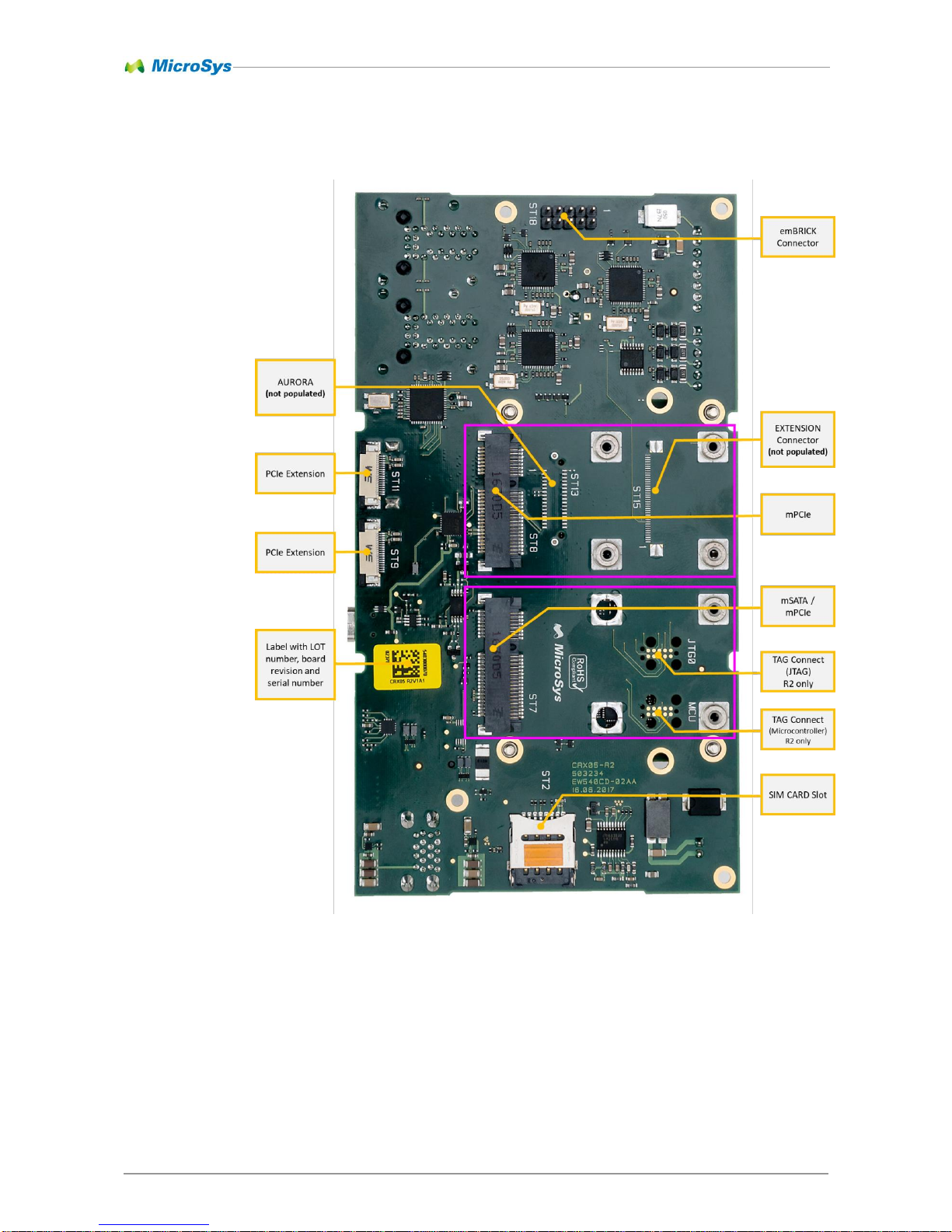
Table 6-1 Connector reference overview

Peripherals 6
miriac SBC-T1024 User Manual
V 2.3
35/70
© MicroSys Electronics GmbH 2017
6.2 Module Connector
The carrierboard CRX05 provides a connector “ST4” which accepts compatible
CPU modules from the MicroSys MPX2-family.
Manufacturer:
JAE
Type:
MM70-314-310-B1-1-R300
Used with:
MicroSys MPX2 module family
6.3 LAN Connections
The SBC-T1024 system offers four independent Gigabit LAN connections. These
four ports are distributed over two connectors named “LAN1” and “LAN2”. The connectors have integrated magnetics.
The following picture shows the front view of the two connectors as placed on the
CRX05 baseboard. For further information on the LEDs please see chapter 8
Part Reference:
LAN1, LAN2
Manufacturer:
Würth Elektronik
Type:
749 915 1120
Mates with:
RJ45 patch ca-
ble, category
depending on
speed
Port
T1024
connection
Serdes Lane
on ST4
RGMII
on ST4
PHY address
1
---
---
---
0000
2
---
---
---
0001 3 ---
---
---
0010
4
„DTSEC4“
---
RGMII1
0011
Table 6-2 LAN / DTSEC / SerDes / RGMII assignment

Peripherals 6
miriac SBC-T1024 User Manual
V 2.3
36/70
© MicroSys Electronics GmbH 2017
The LAN Sockets have a standard layout for GBit Ethernet, i.e. the pairs are 1-2, 36, 4-5 and 7-8.
Pin
Pair 1 D-A+ 2 D-A- 3 D-B+ 4 D-C+ 5 D-C- 6 D-B- 7 D-D+ 8 D-D-
Table 6-3 LAN Gigabit Ethernet connector pairs
6.3.1 Port 1 / 2 / 3
Port 1, 2 and 3 are SGMII ports which are not supported by the evaluation board
SBC-T1024.
6.3.2 Port 4
Port 4 is connected to a standard RJ-45 socket “LAN2”. It uses the Ethernet
controller EC1 as RGMII port provided by the T1024 CPU. The RGMII lanes
connect to a Marvell PHY 88E1512P which uses a copy of the reference voltage on
pin T80 of the module connector ST4 as I/O voltage (1.8V).
The following table shows the internal connections for Port 4.
I/O
Range
88E1512P
ST4 T1024
Pull-
up
Pull-
down
Pin
Name
Pin
Signal
Pin
Name
1.8V 46
RX_CLK
→
T86
MII1-
RXCK
→
AD1
MII_RX_CLK
1.8V 43
RX_CTRL
→
T95
MII1-
RXDV
→
AG2
MII_RX_DV
1.8V 44
RXD0
→
T88
MII1-
RXD0
→
AF2
MII_RXD0
1.8V
4k7 45
RXD1
→
T89
MII1-
RXD1
→
AF1
MII_RXD1
1.8V 47
RXD2
→
T91
MII1-
RXD2
→
AE1
MII_RXD2
1.8V 48
RXD3
→
T92
MII1-
RXD3
→
AD2
MII_RXD3
1.8V 53
TX_CLK
←
T94
MII1-
TXCK
←
AF3
MII_TX_CLK
1.8V 50
TXD0
←
T97
MII1-
TXD0
←
AE3
MII_TXD0
1.8V 51
TXD1
←
T98
MII1-
TXD1
←
AE4
MII_TXD1
1.8V 54
TXD2
←
T100
MII1-
TXD2
←
AD3
MII_TXD2
1.8V 55
TXD3
←
T101
MII1-
TXD3
←
AC3
MII_TXD3

Peripherals 6
miriac SBC-T1024 User Manual
V 2.3
37/70
© MicroSys Electronics GmbH 2017
I/O
Range
88E1512P
ST4 T1024
Pull-
up
Pull-
down
Pin
Name
Pin
Signal
Pin
Name
1.8V
4k7 56
TX_CTRL
←
T103
MII1-
TXEN
←
AF4
MII_TXEN
1.8V
5k0
8
MDIO
↔
B87
MII1-
MDIO
↔
AH4
EMI1_MDIO
1.8V
10k0
7
MDC
←
B86
MII1MDC
←
AH3
EMI1_MDC
1.8V 9
CLK125
→
T83
MII1-
CRS
→
AG3
EC1_GTX_CLK125
Table 6-4 Port4 pin assignment

Peripherals 6
miriac SBC-T1024 User Manual
V 2.3
38/70
© MicroSys Electronics GmbH 2017
6.4 PCIe Connections
The SBC-T1024 offers two x1 lanes on the following connectors.
Table 6-5 PCIe SerDes assignment
Basically, the carrierboard offers four x1 lanes on different connectors which may
be available in combination with other MPX2 modules.
6.4.1 Mini-PCIe Slot
There are two mini PCIe slot on the carrierboard.
The first one can hold mPCIe cards only, mSATA is not supported.
Part Reference:
ST8
Manufacturer:
Tyco
Type:
2041119-1
Used with:
Half size mini PCIe
cards are preferred
Broaching nuts for both half and full
size cards are placed on the carrier
board. When full size cards are
used care has to be taken to
choose cards that do not have parts
on the bottom side accidentally
shorting signals.
MicroSys recommends to use half
size cards with this slot only!
Serdes
ST7
(Mini-PCIe /
mSATA Slot)
ST8
(Mini PCIe Slot)
ST9
(PCIe Extension
Connector)
ST11
(PCIe Extension
Connector)
Lane 0
Not available with
the SBC-T1024
Lane 4
✓
Lane 5
✓
Lane 7
Not available with
the SBC-T1024

Peripherals 6
miriac SBC-T1024 User Manual
V 2.3
39/70
© MicroSys Electronics GmbH 2017
Pin:
Pin:
1
WAKE#
+3.3Vaux
2
3
COEX1
GND
4 5 COEX2
+1.5V
6 7 CLKREQ#
UIM-PWR
8 9 GND
UIM-DAT
10
11
REFCLK-
UIM-CLK
12
13
REFCLK+
UIM-RST
14
15
GND
UIM-VPP
16
MECHANICAL KEY
17
Reserved
GND
18
19
Reserved
WDIS#
20
21
GND
PERST#
22
23
PER0-
+3.3Vaux
24
25
PER0+
GND
26
27
GND
+1.5V
28
29
GND
SMB-CLK
30
31
PET0-
SMB-DAT
32
33
PET0+
GND
34
35
GND
USB-D-
36
37
GND
USB-D+
38
39
+3.3Vaux
GND
40
41
+3.3Vaux
LED-WWAN#
42
43
GND
LED_WLAN#
44
45
Reserved
LED_WPAN#
46
47
Reserved
+1.5V
48
49
Reserved
GND
50
51
Reserved
+3.3Vaux
52
Table 6-6 mPCIe Slot pinout
The following table shows the internal connections:
ST8 ST4 T1024
Pin
Name
Pin
Signal
Pin
Name
33
PET4+
←
T23
SRD-TX4+
←
AD11
SD-TX4
31
PET4-
←
T24
SRD-TX4-
←
AE11
SD-TX4#
25
PER4+
→
T20
SRD-RX4+
→
AH11
SD-RX4
23
PER4-
→
T21
SRD-RX4-
→
AG11
SD-RX4#
Table 6-7 mPCIe Slot SerDes 4 assignment

Peripherals 6
miriac SBC-T1024 User Manual
V 2.3
40/70
© MicroSys Electronics GmbH 2017
6.4.2 Mini-PCIe Slot / mSATA Slot
The mPCIe / mSATA slot is not connected on the SBC-T1024 and therefore can not be
used.
Basically, the second slot can hold both mSATA cards and mPCIe cards.
It may be available in combination with other MPX2 modules.
Part Reference:
ST7
Manufacturer:
Tyco
Type:
2041119-1
Used with:
Full size or half size
mini PCIe or
mSATA cards
Four holes for broaching nuts are
designed to allow for half and full
size cards to be used with this slot.
The broaching nuts for half size
cards are not populated as
standard to allow cards without
height restrictions.
Revision 3 has NO connector JTG0
and MCU in this area!

Peripherals 6
miriac SBC-T1024 User Manual
V 2.3
41/70
© MicroSys Electronics GmbH 2017
Pin:
Pin:
1
WAKE#
+3.3Vaux
2 3 COEX1
GND
4 5 COEX2
+1.5V
6
7
CLKREQ#
UIM-PWR
8 9 GND
UIM-DAT
10
11
REFCLK-
UIM-CLK
12
13
REFCLK+
UIM-RST
14
15
GND
UIM-VPP
16
MECHANICAL KEY
17
Reserved
GND
18
19
Reserved
WDIS#
20
21
GND
PERST#
22
23
PER0+
+3.3Vaux
24
25
PER0-
GND
26
27
GND
+1.5V
28
29
GND
SMB-CLK
30
31
PET0-
SMB-DAT
32
33
PET0+
GND
34
35
GND
USB-D-
36
37
GND
USB-D+
38
39
+3.3Vaux
GND
40
41
+3.3Vaux
LED-WWAN#
42
43
GND
LED_WLAN#
44
45
Reserved
LED_WPAN#
46
47
Reserved
+1.5V
48
49
Reserved
GND
50
51
Reserved
+3.3Vaux
52
Table 6-8 mPCIe / mSATA Slot pinout
The following table shows the internal connections:
ST7 ST4 T1024
Pin
Name
Pin
Signal
Pin
Name
33
PET0+
←
T5
SRD-TX7+
← - -
31
PET0-
←
T6
SRD-TX7-
← - -
23
PER0-
→
T2
SRD-RX7+
→ - -
25
PER0+
→
T3
SRD-RX7-
→ - -
Table 6-9 mPCIe Slot SerDes 7 assignment (not connected)

Peripherals 6
miriac SBC-T1024 User Manual
V 2.3
42/70
© MicroSys Electronics GmbH 2017
6.4.3 PCIe Extension Connector 1
ST9 is not connected on the SBC-T1024 and therefore can not be used.
Part Reference:
ST9
Manufacturer:
Würth Elektronik
Type:
687 118 140 22
Mates with:
FFC cable, 18pins,
pitch 0.5mm
Pin:
1
+3.3V
2
+3.3V
3
+3.3V
4
+1.5V
5
GND
6
REFCLK-
7
REFCLK+
8
GND
9
PER0-
10
PER0+
11
GND
12
PET0-
13
PET0+
14
GND
15
I2C2D-SCL
16
I2C2D-SDA
17
GND
18
PERST#
Table 6-10 PCIe Extension connector pinout (ST9)
The following table shows the internal connections:
ST9 ST4 T1024
Pin
Name
Pin
Signal
Pin
Name
13
PET0+
←
T47
SRD-TX0+
← - -
12
PET0-
←
T48
SRD-TX0-
← - -
10
PER0+
→
T44
SRD-RX0+
→ - -
9
PER0-
→
T45
SRD-RX0-
→ - -
Table 6-11 PCIe Edge Card connector SerDes 0 assignment

Peripherals 6
miriac SBC-T1024 User Manual
V 2.3
43/70
© MicroSys Electronics GmbH 2017
6.4.4 PCIe Extension Connector 2
The PCIe Extension Connectors “ST9” and “ST11” provide basic PCIe signals.
They have identical pinouts providing power, data, clock, reset and I²C signals.
Depending on the module and software configuration the data signals can also be
used for other interfaces according to the SerDes configuration of the respective
module.
The extension connectors interface the CRX05 carrier board with any specially
developed adapter. No standard pinout is used.
Part Reference:
ST11
Manufacturer:
Würth Elektronik
Type:
687 118 140 22
Mates with:
FFC cable, 18pins,
pitch 0.5mm
The I2C port is accessible via I2C Bus 2 and the I2C multiplexer TCA9544A (address
0x70). See chapter 5.8.2 for more information.
Devices connected to ST9 and ST11 share channel 3.
Pin:
1
+3.3V
2
+3.3V
3
+3.3V
4
+1.5V
5
GND
6
REFCLK-
7
REFCLK+
8
GND
9
PER0-
10
PER0+
11
GND
12
PET0-
13
PET0+
14
GND
15
I2C2D-SCL
16
I2C2D-SDA
17
GND
18
PERST#
Table 6-12 PCIe Extension connector pinout (ST11)

Peripherals 6
miriac SBC-T1024 User Manual
V 2.3
44/70
© MicroSys Electronics GmbH 2017
The following table shows the internal connections:
ST11 ST4 T1024
Pin
Name
Pin
Signal
Pin
Name
13
PET0+
←
T17
SRD-TX5+
←
AD17
SD-TX5
12
PET0-
←
T18
SRD-TX5-
←
AE17
SD-TX5#
10
PER0+
→
T14
SRD-RX5+
→
AH17
SD-RX5
9
PER0-
→
T15
SRD-RX5-
→
AG17
SD-RX5#
Table 6-13 PCIe Edge Card connector SerDes 5 assignment
6.4.5 PCIe with external clock
To run board with external PCIe clock board has to be modified on assembly level.
Please contact MicroSys if required.

Peripherals 6
miriac SBC-T1024 User Manual
V 2.3
45/70
© MicroSys Electronics GmbH 2017
6.5 SATA
The SATA port is not available with the SBC-T1024 system.
Part Reference:
ST10
Manufacturer:
3M
Type:
5607-4200-SH
Used with:
SATA cable (7pin)
The following table shows the internal connections:
ST10 ST4 T1024
Pin
Name
Pin
Signal
Pin
Name
1 GND 2
A+
←
T11
SRD-TX6+
← - - 3
A-
←
T12
SRD-TX6-
← - - 4
GND 5
B- → T9
SRD-RX6-
→ - - 6
B+ → T8
SRD-RX6+
→ - -
7
GND
Table 6-14 SATA connector pin assignment (not connected)

Peripherals 6
miriac SBC-T1024 User Manual
V 2.3
46/70
© MicroSys Electronics GmbH 2017
6.6 MicroSD Card Slot
The SBC-T1024 system offers a microSD Card slot.
The microSD card can also be configured as a boot device.
Part Reference:
ST1
Manufacturer:
Yamaichi
Type:
PJS-008-2130-0
Used with:
microSD cards
The following table shows the connections of the microSD card slot:
I/O
Range
ST1 ST4 T1024
Pin
Name
Pin
Signal
Pin
Name
LVTTL 1 DAT2
↔
B96
SDC-D2
↔
L3
SDHC_DAT2
LVTTL
2
CD/DAT3
↔
B95
SDC-D3
↔
L1
SDHC_DAT3
LVTTL 3 CMD
↔
B99
SDC-CMD
↔
K3
SDHC_CMD
4 Vdd
LVTTL 5 CLK
←
B100
SDC-CLK
←
K1
SDHC_CLK
6 Vss
LVTTL 7 DAT0
↔
B98
SDC-D0
↔
L2
SDHC_DAT0
LVTTL 8 DAT1
↔
B97
SDC-D1
↔
K4
SDHC_DAT1
LVTTL 9 SW1
→
B90
SDC-CD#
→
L5
SDHC_CD#
LVTTL
10
SW2
→
B89
SDC-WP
→
M5
SDHC_WP
Table 6-15 microSD card slot pin assignment
The microSD card slot uses a copy of the reference voltage on pin B81 of the module
connector ST4 as I/O voltage (3.3V).
This voltage is generated on the carrierboard.

Peripherals 6
miriac SBC-T1024 User Manual
V 2.3
47/70
© MicroSys Electronics GmbH 2017
6.7 USB
The SBC-T1024 system features a stacked USB connector for two ports.
The SBC-T1024 module does not support USB3.0 (super speed)
Part Reference:
ST6
Manufacturer:
Würth Elektronik
Type:
692 141 030 100
Mates with:
USB Type A
cables
6.7.1 USB1
The following table shows the internal connections:
ST6 (Bottom)
ST4 T1024
Pin
Signal Pin
Signal
Pin
Name
1
Vbus+
→
B133
USB1-VBUS
→
E4
USB1_VBUSCLMP
2
D- ↔ T131
USB1-D-
↔
F2
USB1_UDM
3
D+ ↔ T130
USB1-D+
↔
F1
USB1_UDP
4
GND
5
SSRX-
→
T118
USB1-SSRX+
--
6
SSRX+
→
T119
USB1-SSRX-
--
7
GND
8
SSTX-
←
T122
USB1-SSTX-
--
9
SSTX+
←
T121
USB1-SSTX+
--
J4
Pin
Signal
4
ENABLE
←
B132
USB1-EN
←
F6
USB1_DRVVBUS
3
FAULT#
→
B131
USB1-OC
→
F5
USB1_PWRFAULT
→
B130
USB1-UID
→
F4
USB1_UID
Table 6-16 USB Host-Only Port 1 pin assignment
USB port 1 can be individually enabled and has a separate overcurrent signal.
USB1_PWRFAULT is a high-active signal. A logic high level signals the port is in an
overcurrent situation
USB2
USB1

Peripherals 6
miriac SBC-T1024 User Manual
V 2.3
48/70
© MicroSys Electronics GmbH 2017
6.7.2 USB2
The following table shows the internal connections:
ST6 (Top) ST4 T1024
Pin
Signal Pin
Signal
Pin
Name
1
Vbus+
→
B128
USB2-VBUS
→
J4
USB2_VBUSCLMP
2
D- ↔ T128
USB2-D-
↔
H2
USB2_UDM
3
D+ ↔ T127
USB2-D+
↔
H1
USB2_UDP
4
GND
5
SSRX-
→
T112
USB2-SSRX+
--
6
SSRX+
→
T113
USB2-SSRX-
--
7
GND
8
SSTX-
←
T116
USB2-SSTX-
--
9
SSTX+
←
T115
USB2-SSTX+
--
J5
Pin
Signal
4
ENABLE
←
B127
USB2-EN
←
J5
USB2_DRVVBUS
3
FAULT#
→
B126
USB2-OC
→
H5
USB2_PWRFAULT
→
B125
USB2-UID
→
H4
USB2_UID
Table 6-17 USB Host-Only Port 2 pin assignment
USB port 2 can be individually enabled and has a separate overcurrent signal.
USB2_PWRFAULT is a high-active signal. A logic high level signals the port is in an
overcurrent situation

Peripherals 6
miriac SBC-T1024 User Manual
V 2.3
49/70
© MicroSys Electronics GmbH 2017
6.7.3 USB3
USB port 3 is not a native USB port of the CPU but converted from UART1 by
means of a FT232RQ chip.
USB3 is available on an USB mini connector type B.
The port is used as the debug port of the T1024.
Part Reference:
ST5
Manufacturer:
Würth Elektronik
Type:
651 005 161 21
Used with:
Mini USB type B
cables
The following table shows the internal connections:
ST5 ST4 T1024
Pin
Signal Pin
Signal
Pin
Name
1
Vbus+ B37
UART1-RXD
→
AA1
UART1_SIN
2
D-
J1
B38
UART1-TXD
←
AA2
UART1_SOUT
3
D+
B39
UART1-CTS#
→
Y2
UART1_CTS#
4
ID B40
UART1-RTS#
←
Y1
UART1_RTS#
5
GND
Table 6-18 USB Host-Only Port 3 pin assignment

Peripherals 6
miriac SBC-T1024 User Manual
V 2.3
50/70
© MicroSys Electronics GmbH 2017
6.8 UART
The SBC-T1024 system is provided with one serial port (UART).
UART1 is converted to USB. See chapter 6.7.3 for details.
UART2 is available on the following extension connector including hardware
handshaking with RTS/CTS. The I/O range is LVTTL.
For RS232 or RS485 additional transceivers are necessary.
They are not implemented on the SBC-T1024 system.
Part Reference:
ST12
Manufacturer:
Würth Elektronik
Type:
648 106 131 822
Mates with:
648 006 113 322
ST12 ST4 T1024
Pin
Signal
Pin
Signal
Pin
Name
1
+3.3V
2
UART2-RXD
→
B32
UART2-RXD
→
W4
UART2_SIN
3
UART2-TXD
←
B33
UART2-TXD
←
AA4
UART2_SOUT
4
UART2-RTS#
←
B35
UART2-RTS#
←
V4
UART2_RTS#
5
UART2-CTS#
→
B34
UART2-CTS#
→
Y4
UART2_CTS#
6
GND
Table 6-19 UART2 pin assignment

Peripherals 6
miriac SBC-T1024 User Manual
V 2.3
51/70
© MicroSys Electronics GmbH 2017
6.9 MCU Connector
The connector “MCU” is for production test R2 only. Not available on CRX05R3.
Part Reference:
MCU
Manufacturer:
Tag-Connect
Type:
TC2050-IDC-FP
MCU
Pin
Signal
1
Please
contact
MicroSys
2 3 4
5
6 7 8
9
10
Table 6-20 MCU Connector Pinout
Pin1
Pin5
Pin6
Pin10

Peripherals 6
miriac SBC-T1024 User Manual
V 2.3
52/70
© MicroSys Electronics GmbH 2017
6.10 JTAG Connector
6.10.1 JTAG on Revision R3
The JTAG signals are available on JST-BM14B-SRSS-TB connector.
Part Reference:
JTG0
Manufacturer:
JST
Type:
BM14B-SrSS-TB
JTG0 ST4 LS1046A
Pin
Signal
Pin
Signal
Pin
Signal
1
JTDO
←
B104
JTDO ← E20
TDO
2
GND 3 JTDI
→
B103
JTDI → G17
TDI
4
TRST#
→
B106
TRST#
→
E19
TRST#
5
+1,8V 6 -
7
JTCK
→
B105
JTCK → E18
TCK
8
HRST#
↔
B111
HRST# ↔ F8
HRESET#
9
JTMS
→
B102
JTMS → G18
TMS
10
GND
11
PRST#
→
B110
PRST# → F9
PORESET#
12
GND
13
MCU-
UART-RDD
→
B114
MCU-
UART-RDD
→
46
J11
MK02FN64VLH10
14
MCU-
UART-TXD
←
B113
MCU-
UART-TXD
←
49
J11
MK02FN64VLH10
Table 6-21 JTAG Connector Pinout R3
Pin1

Peripherals 6
miriac SBC-T1024 User Manual
V 2.3
53/70
© MicroSys Electronics GmbH 2017
6.10.2 JTAG on Revision R2
The JTAG signals are available on a TAG connect footprint.
Part Reference:
JTG0
Manufacturer:
Tag-Connect
Type:
TC2050-IDC-FP
JTG0 ST4 T1024
Pin
Signal
Pin
Signal Pin
Signal
1
JTMS
→
B102
JTMS → B18
TMS
2
HRST#
↔
B111
HRST# ↔ E8
HRESET#
3
+1,8V
4
TRST#
→
B106
TRST#
→
D19
TRST#
5
JTDO
←
B104
JTDO ← C18
TDO
6
JTCK
→
B105
JTCK → E18
TCK
7
GND
8
PRST#
→
B110
PRST#
→
F13
PORESET#
9
JTDI
→
B103
JTDI → A18
TDI
10
n.c.
Table 6-22 JTAG Connector Pinout
Pin1
Pin5
Pin6
Pin10

Peripherals 6
miriac SBC-T1024 User Manual
V 2.3
54/70
© MicroSys Electronics GmbH 2017
6.11 Aurora Connectors (optional)
In order to use the Aurora interface hardware modifications are required.
The Aurora connectors are not populated by default.
Part Reference:
ST13
Manufacturer:
Samtec
Type:
ASP-137973-01
Pin:
Pin:
1
TX0+
VREF (1,8V)
2 3 TX0-
TCK
4 5 GND
TMS
6 7 TX1+
TDI
8
9
TX1-
TDO
10
11
GND
TRST#
12
13
TX2+
HALT#
14
15
TX2-
EVTI#
16
17
GND
EVTO#
18
19
TX3+
GEN_IO3
20
21
TX3-
RST#
22
23
GND
GND
24
25
TX4+
CLK+
26
27
TX4-
CLK-
28
29
GND
GND
30
31
TX5+
RDY#
32
33
TX5-
HRST#
34
Table 6-23 Aurora Connector Pinout
The module standard connector pinout (ST4) does not provide all signals which are
necessary for the Aurora interface. Additional signals are available on the following
connector “ST14”. For more information please contact MicroSys.
Part Reference:
ST14
Manufacturer:
JST
Type:
SM06B-XSRS-ETB
Mates with:
06XSR-36S
Pin
Signal
1
HALT#
2
EVTI#
3
EVTO# 4 - 5 - 6 -
Table 6-24 Aurora Connector (ST14) Pinout
Peripherals 6
miriac SBC-T1024 User Manual
V 2.3
55/70
© MicroSys Electronics GmbH 2017
6.12 General Purpose Inputs / Outputs
The functional scope of the carrierboard has been extended by GPIOs which
support a maximum of 24V at the input. The maximum output level depends on the
input voltage which is limited to 24V. For lower input voltages an external voltage
up to 24V can alternatively be supplied. In that case a hardware modification is
necessary.
Inputs and outputs are controlled by a MAX7325ATG I²C GPIO Expander. The
output pins are level shifted to either the input voltage or to the level of an
externally supplied voltage. The output driver can be separately enabled and
disabled. Additionally a fault pin exists that signals a chip thermal shutdown or an
overcurrent condition on any channel.
MAX7325ATG
Description
P6 (Pin7)
FAULT input: Logic low signals fault event
O14 (Pin16)
A logic high enables the GPOUT driver
GPINs:
Part Reference:
ST16
Manufacturer:
Würth Elektronik
Type:
691 382 010 006
Mates with:
691 381 000 006
Pin:
Description
MAX7325ATG
1
IN0
P0 (Pin1)
2
IN1
P1 (Pin2)
3
IN2
P2 (Pin3)
4
IN3
P3 (Pin4)
5
IN4
P4 (Pin5)
6
IN5
P5 (Pin6)
Table 6-25 GPIN connector pinout (ST16)

Peripherals 6
miriac SBC-T1024 User Manual
V 2.3
56/70
© MicroSys Electronics GmbH 2017
GPOUTs:
Part Reference:
ST17
Manufacturer:
Würth Elektronik
Type:
691 382 010 008
Mates with:
691 381 000 008
Pin:
Description
MAX7325ATG
1
+VIN / +VEXT
-
2
OUT6
Maximum output
current on all ports
together: 350mA
O13 (Pin15)
3
OUT5
O12 (Pin14)
4
OUT4
O11 (Pin13)
5
OUT3
O10 (Pin12)
6
OUT2
O9 (Pin11)
7
OUT1
O8 (Pin10)
8
GND
-
Table 6-26 GPOUT connector pinout (ST17)
Pin 1 of connector ST17 is connected to the carrierboard input voltage via R154.
In order to supply the GPOUT section with input voltages different from the input
voltage R154 has to be removed. V_EXT on pin1 supports input voltages from 5V to
24V.

Peripherals 6
miriac SBC-T1024 User Manual
V 2.3
57/70
© MicroSys Electronics GmbH 2017
6.13 Fan Connector
The SBC-T1024 provides a fan connector marked with „PWE“.
In case a fan is necessary MicroSys recommends to use a 5V rated fan.
Part Reference:
PWE
Manufacturer:
Würth Elektronik
Type:
679 304 124 022
Mates with:
648 004 113 322
Pin:
Description
1
+5V 2 GND
3
GND
4
+VIN
Table 6-27 FAN connector pinout (PWE)

Peripherals 6
miriac SBC-T1024 User Manual
V 2.3
58/70
© MicroSys Electronics GmbH 2017
6.14 Smart Card Connector
THE SMART CARD INTERFACE IS CURRENTLY NOT SUPPORTED
Part Reference:
ST2
Manufacturer:
Würth Elektronik
Type:
693 022 010 811
Mates with:
t.b.d.
Connection von CRX05-R3, not available on CPU
ST2 ST4
T1024
Pin
Signal
Name
Pin
Description
Pin
Signal
Name
1
+3,3V - 2 RST
←
B121
10k PU
←
-
-
3
CLK
←
B122
10k PU
←
-
-
4 - -
5
GND - 6 - - 7 I/O
↔
B123
10k PU
↔
- - 8 - -
Table 6-28 Smart Card connector pinout (ST2) for CRX05-R3
Connection von CRX05-R2:
ST2 ST4
T1024
Pin
Signal
Name
Pin
Description
Pin
Signal
Name
1
+3,3V - 2 RST
←
Pin B67
10k PU
←
U2
GPIO4_10
3
CLK
←
Pin B66
10k PU
←
U1
GPIO4_11
4
n.c. -
5
GND - 6 n.c. - 7 I/O
↔
Pin B65
10k PU
↔
T1
GPIO4_12
8
n.c. -
Table 6-29 Smart Card connector pinout (ST2) for CRX05-R2

Peripherals 6
miriac SBC-T1024 User Manual
V 2.3
59/70
© MicroSys Electronics GmbH 2017
6.15 emBRICK Connector
THE emBRICK INTERFACE IS CURRENTLY NOT SUPPORTED
Part Reference:
ST18
Manufacturer:
Würth Elektronik
Type:
613 005 211 21
Mates with:
Standard 2.54mm
dual row socket
Pin
Signal Name
Connection
1
SEL_OUT
MAX7325ATG
O15 (Pin17)
2
MOSI#
SC18IS602BIPW
MOSI (Pin6)
3
MISO#
SC18IS602BIPW
MISO (Pin5)
4
CLK#
SC18IS602BIPW
SPICLK (Pin11)
5
+3,3V
6
GND
7
GND
8
GND
9
+VIN
10
+VIN
Table 6-30 emBRICK connector pinout (ST18)

Switches, Buttons and Jumpers 7
miriac SBC-T1024 User Manual
V 2.3
60/70
© MicroSys Electronics GmbH 2017
7 Switches, Buttons and Jumpers
7.1 Boot Device Switch
The boot device can be selected by the switch “SW1”.
The boot device switches implement a maximum of four possible boot devices. The
following boot devices are supported by the T1024:
SW1 inverts the logic levels of the BOOT-SELx pins. By setting the switch to ON the
corresponding pin is actually pulled low (grounded).
The following table shows the internal connections of the BOOT-SEL pins:
SW1 ST4
Microcontroller
Switch
Signal
Pin
Signal
Pin
Name
1-1
BOOT-SEL1
→
T134
BOOT-SEL1
→
19
PTA17
1-2
BOOT-SEL2
→
T133
BOOT-SEL2
→
20
PTA18
Table 7-2 BOOT-SELx pin assignment
Setting
SW 1-1
SW 1-2
Boot
device
Features
Boot
location
OFF
OFF
SPI
Flash
NAND flash is connected to CS1#
module
OFF
ON
NAND
Flash
NAND flash is connected to CS0#
module
ON
OFF
microSD
Card
SD/MMC interface: 8 bit
board
ON
ON
microSD
Card
SD/MMC interface: 4 bit
board
Table 7-1 Boot device settings
Figure 7-1 Boot Device Switch

Switches, Buttons and Jumpers 7
miriac SBC-T1024 User Manual
V 2.3
61/70
© MicroSys Electronics GmbH 2017
7.2 Board Configuration Switch
The board configuration switch influences the behavior of the watchdog and the I²C
address of the EEPROM on I²C Bus1:
Setting
SW 2-1
SW 2-2
Description
OFF - Watchdog disabled
ON - Watchdog active
-
OFF
EEPROM J25: address 0x57
-
ON
EEPROM J25: address 0x55
Table 7-3 Configuration switch settings
7.3 PCIe selection: root complex / endpoint
The PCIe configuration switch influences the behavior of root complex or endpoint.
Figure 7-2 Board Configuration Switch
Figure 7-3 PCIe selection Switch
Switches, Buttons and Jumpers 7
miriac SBC-T1024 User Manual
V 2.3
62/70
© MicroSys Electronics GmbH 2017
Setting
SW 4-1
SW 4-2
Description
OFF - PCIe = root complex
ON - PCIe = endpoint
-
OFF
Not used
-
ON
Not used
Table 7-4 PCIe configuration switch settings
7.4 Reset Button
Pressing the reset switch “SW3” triggers a Hard Reset.
SW3 is connected to the reset input of a MAX6751KA29 chip via additional logic.
The resulting open drain reset signal is then inverted and fed to the microcontroller.
The following table shows the internal connections:
SW3
J17 ST4
Microcontroller
Pin
Signal
Pin Pin
Signal
Pin
Name
1 & 3
+3,3V
2 & 4
RST-
BTN
($39166)
→ 1
7 →
T136
RST-IN#
→ 2 PTB7
Table 7-4 Reset button pinout
Figure 7-3 Reset Button

LEDs 8
miriac SBC-T1024 User Manual
V 2.3
63/70
© MicroSys Electronics GmbH 2017
8 LEDs
8.1 RJ45 LEDs
The following table summarizes the RJ45 LEDs of the SBC-T1024:
Part
Reference
Source
Signal Name
Function
LAN1-A
J8
LAN1-LED0
Green LED: configurable
Default: 3 blinks – 1000Mbps / 2 blinks – 100 Mbps
/ 1 blink – 10 Mbps / 0 blinks – no link
LAN1-A
J8
LAN1-LED2
Yellow LED: off
LAN1-B
J10
LAN2-LED1
Green LED: configurable
Default: On = Link / Off = no Link / Blink = Activity
LAN1-B
J10
LAN2-LED2
Yellow LED: off
LAN2-B
J12
LAN3-LED0
Green LED: configurable
Default: 3 blinks – 1000Mbps / 2 blinks – 100 Mbps
/ 1 blink – 10 Mbps / 0 blinks – no link
LAN2-B
J12
LAN3-LED2
Yellow LED: off
LAN2-A
J14
LAN4-LED1
Green LED: configurable
Default: On = Link / Off = no Link / Blink = Activity
LAN2-A
J14
LAN4-LED2
Yellow LED: off
Table 8-1 Indicator LEDs
Figure 8-1 RJ 45 LEDs

LEDs 8
miriac SBC-T1024 User Manual
V 2.3
64/70
© MicroSys Electronics GmbH 2017
8.2 Power And Reset LEDs
Part
Reference
Source
Signal Name
Function
LD1
ST3
VEXT
Power (VEXT) On
LD2
ST4
CB-RST#
Carrier board reset active
LD3
J17 / SW3
RST-IN#
• Power on the carrier is not ok
• watchdog reset is active
• manual reset is triggered
Table 8-2 Indicator LEDs - Carrier board
Colour
Function
Green
LED ON: Power-up sequence of the module is finished, power is good
LED OFF: Power fail
Red
LED ON: Module reset is active
LED OFF: Reset is inactive
Table 8-3 Indicator LEDs – Module

LEDs 8
miriac SBC-T1024 User Manual
V 2.3
65/70
© MicroSys Electronics GmbH 2017
8.3 RGB LEDs
The SBC-T1024 provides a RGB LED driver controlling four RGB LEDs.
I²C address 0x68 is existing twice on I2C-1 bus.
Therefore, the so-called “All Call I2C address” of the TLC59116IRHBR RGB LED
driver has to be disabled before GP input pins of the MAX7325 port expander can be
read correctly. This can be achieved by setting the default value 1 of Bit 0 in MODE1
register to 0.
The following table shows how the LEDs are mapped to the driver outputs:
Part
Reference
LED Driver Output
LED Output Register
LD4
LED0
0x14
LED1
LED2
LED3 is not connected
LD7
LED4
0x15
LED5
LED6
LED7 is not connected
LD6
LED8
0x16
LED9
LED10
LED11 is not connected
LD5
LED12
0x17
LED13
LED14
LED15 is not connected

Software 9
miriac SBC-T1024 User Manual
V 2.3
66/70
© MicroSys Electronics GmbH 2017
9 Software
9.1 U-Boot
The SBC-T1024 uses an U-Boot as standard boot loader, which is always
integrated in both the board's NAND and SPI Flash memories on delivery.
Additionally, there’s an U-Boot version available to be placed on microSD card, if
both other boot options should fail for some reason.
Either boot option can be selected by the Boot Device Switch (see chapter 7).
9.2 Operating System Support
MicroSys Electronics GmbH offers Linux and Microware OS-9 RTOS support for
the board.
Other Operating Systems are available on request only.
If you should have ordered a Starter Kit, the most recent Linux will already be
installed in the board's flash, so you can start to develop and test your application
right away.
9.3 Flash Layout
9.3.1 NAND Flash
Start
End
Definition
Size
0x000000
0x0FFFFF
u-boot
1MB
0x100000
0x11FFFF
u-boot env
128KB
0x160000
0x16FFFF
FMAN Ucode
64KB
0x180000
0x18FFFF
QE Firmware
64KB
Table 9-1 NAND Flash Memory Map
9.3.2 SD Card
Block
# Blocks
Definition
Size
0x008
2048
u-boot
1MB
0x800
0024
u-boot env
8KB
0x820
0256
FMAN Ucode
128KB
0x920
0256
QE Firmware
128KB
Table 9-2 SD Card Memory Map
9.3.3 SPI Flash
Start
End
Definition
Size
0x000000
0x0FFFFF
u-boot
1MB
0x100000
0x101FFF
u-boot env
8KB
0x110000
0x12FFFF
FMAN Ucode
128KB
0x130000
0x14FFFF
QE Firmware
128KB
Table 9-3 SPI Flash Memory Map

Appendix 10
miriac SBC-T1024 User Manual
V 2.3
67/70
© MicroSys Electronics GmbH 2017
10 Appendix
10.1 Acronyms
These acronyms are being used within the document; note that this list does not
claim to be complete or exhaustive:
CPU ............................................................................................... Central Processing Unit
DC ................................................................................................................. Direct Current
DDR4 ............................................................ Double Data Rate Memory fourth-generation
EC ......................................................................................................... Ethernet Controller
EEPROM ..................................... Electrically Erasable Programmable Read-only Memory
ESD ................................................................................................ Electrostatic Discharge
Gbps ...................................................................................................... Gigabit per second
GND ........................................................................................................................ Ground
GPL ................................................................................................ General Public License
I2C ................................................................................................... Inter-Integrated Circuit
JTAG .............................................................................................. Joint Test Action Group
LAN ...................................................................................................... Local Area Network
LED ..................................................................................................... Light Emitting Diode
LVTTL .................................................................. Low Voltage Transistor–Transistor Logic
MCU ..................................................................................................... Microcontroller Unit
MMC .......................................................................................................... Multimedia Card
mPCIe ................................................... Mini Peripheral Component Interconnect Express
mSATA ........................................................ Mini Serial Advanced Technology Attachment
PCIe ............................................................. Peripheral Component Interconnect Express
RGMII ......................................................... Reduced Gigabit Media-independent Interface
RTC ........................................................................................................... Real Time Clock
SBC ................................................................................................ Single Board Computer
SD ................................................................................................................. Secure Digital
SDIO ......................................................................................... Secure Digital Input Output
SDRAM .................................................. Synchronous Dynamic Random Access Memory
SOM ......................................................................................................System On Module
SPI .............................................................................................. Serial Peripheral Interface
UART .......................................................... Universal Asynchronous Receiver Transmitter
USB ..................................................................................................... Universal Serial Bus

Appendix 10
miriac SBC-T1024 User Manual
V 2.3
68/70
© MicroSys Electronics GmbH 2017
10.2 Table of Figures
Figure 3-1 System setup example (LAN port 4) ................................................................... 12
Figure 4-1 Block Diagram (MPX-T1024 Revision 4 on carrier CRX05 Revision 2) .............. 15
Figure 4-2 Mechanical Dimensions Modul ........................................................................... 17
Figure 4-3 SBC-T1024 Mechanical Dimensions .................................................................. 18
Figure 4-4 Top connectors ................................................................................................... 19
Figure 4-5 Bottom connectors .............................................................................................. 20
Figure 4-6 Power supply structure ....................................................................................... 22
Figure 5-1 Reset Structure (carrier CRX05 Revision 2) ....................................................... 24
Figure 7-1 Boot Device Switch ............................................................................................. 60
Figure 7-2 Board Configuration Switch ................................................................................ 61
Figure 7-3 Reset Button ....................................................................................................... 62
Figure 8-1 RJ 45 LEDs ......................................................................................................... 63
10.3 Table of Tables
Table 1-1 Symbols ................................................................................................................. 6
Table 1-2 Conventions ........................................................................................................... 6
Table 2-1 Safety and Handling Precautions ........................................................................... 7
Table 2-2 Functional coverage ............................................................................................. 10
Table 4-1 Pinout ST3 ........................................................................................................... 21
Table 5-1 Reset signal overview .......................................................................................... 25
Table 5-2 Voltage monitoring limits (carrier)......................................................................... 26
Table 5-3 Clock distribution and explanation........................................................................ 27
Table 5-4 Hard wired boot signals ........................................................................................ 28
Table 5-5 NAND Flash pin assignments .............................................................................. 29
Table 5-6 SPI Flash pin assignment .................................................................................... 30
Table 5-7 I²C1 bus map ....................................................................................................... 31
Table 5-8 I²C-1 pin assignment ............................................................................................ 32
Table 5-9 I²C2 bus map ....................................................................................................... 32
Table 5-10 I²C-2 pin assignment ................................................................ .......................... 33
Table 6-1 Connector reference overview ............................................................................. 34
Table 6-2 LAN / DTSEC / SerDes / RGMII assignment ....................................................... 35
Table 6-3 LAN Gigabit Ethernet connector pairs .................................................................. 36
Table 6-4 Port4 pin assignment ........................................................................................... 37
Table 6-5 PCIe SerDes assignment ..................................................................................... 38
Table 6-6 mPCIe Slot pinout ................................................................................................ 39
Table 6-7 mPCIe Slot SerDes 4 assignment ........................................................................ 39
Table 6-8 mPCIe / mSATA Slot pinout ................................................................................. 41
Table 6-9 mPCIe Slot SerDes 7 assignment (not connected) .............................................. 41
Table 6-10 PCIe Extension connector pinout (ST9) ............................................................. 42
Table 6-11 PCIe Edge Card connector SerDes 0 assignment ............................................. 42

Appendix 10
miriac SBC-T1024 User Manual
V 2.3
69/70
© MicroSys Electronics GmbH 2017
Table 6-12 PCIe Extension connector pinout (ST11) ........................................................... 43
Table 6-13 PCIe Edge Card connector SerDes 5 assignment ............................................. 44
Table 6-14 SATA connector pin assignment (not connected) .............................................. 45
Table 6-15 microSD card slot pin assignment ...................................................................... 46
Table 6-16 USB Host-Only Port 1 pin assignment ............................................................... 47
Table 6-17 USB Host-Only Port 2 pin assignment ............................................................... 48
Table 6-18 USB Host-Only Port 3 pin assignment ............................................................... 49
Table 6-19 UART2 pin assignment ...................................................................................... 50
Table 6-20 MCU Connector Pinout ...................................................................................... 51
Table 6-21 JTAG Connector Pinout R3 ................................................................................ 52
Table 6-22 JTAG Connector Pinout ..................................................................................... 53
Table 6-23 Aurora Connector Pinout .................................................................................... 54
Table 6-24 Aurora Connector (ST14) Pinout ........................................................................ 54
Table 6-25 GPIN connector pinout (ST16) ........................................................................... 55
Table 6-26 GPOUT connector pinout (ST17) ....................................................................... 56
Table 6-27 FAN connector pinout (PWE) ............................................................................. 57
Table 6-28 Smart Card connector pinout (ST2) for CRX05-R3 ............................................ 58
Table 6-29 Smart Card connector pinout (ST2) for CRX05-R2 ............................................ 58
Table 6-30 emBRICK connector pinout (ST18) .................................................................... 59
Table 7-1 Boot device settings ............................................................................................. 60
Table 7-2 BOOT-SELx pin assignment ................................................................................ 60
Table 7-3 Configuration switch settings ............................................................................... 61
Table 7-4 Reset button pinout .............................................................................................. 62
Table 8-1 Indicator LEDs ..................................................................................................... 63
Table 8-2 Indicator LEDs - Carrier board ............................................................................. 64
Table 8-3 Indicator LEDs – Module ...................................................................................... 64
Table 9-1 NAND Flash Memory Map ................................................................................... 66
Table 9-2 SD Card Memory Map ......................................................................................... 66
Table 9-3 SPI Flash Memory Map ........................................................................................ 66
Table 11-1 Document history ............................................................................................... 70

History 11
miriac SBC-T1024 User Manual
V 2.3
70/70
© MicroSys Electronics GmbH 2017
11 History
Date
Version
Change Description
2017-10-06
2.0
Release Version for carrier CRX05 Revision 2
2017-12-06
2.1
NAND FLASH Memory Map changed
2018-07-16
2.2
Table 2-2: add LED colors
Operating voltage change to 9V – 30V
PCIe portcount correction
2019-01-28
2.3
Added differences CRX05 carrier revision 2 to revision 3 (2.4.1)
Table 11-1 Document history
 Loading...