

Page 1
Creating Embedded Systems
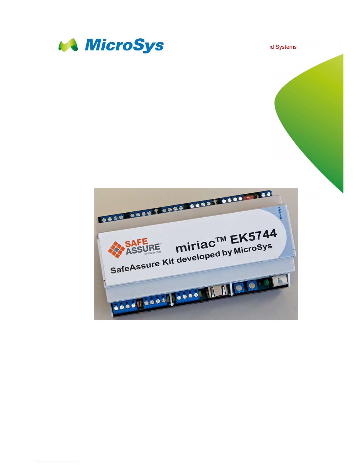
miriac EK5744
User Manual
V 1.2
Page 2

Table of Contents
miriac EK
-
5744 User Manual
V 1.2 2/53
© MicroSys Electronics GmbH 2017
Table of Contents
1 General Notes .............................................. 3
1.1 Warranty ........................................................ 3
1.2 Links .............................................................. 3
1.3 Liability .......................................................... 3
1.4 Offer to Provide Source Code of Certain
Software ........................................................ 4
1.5 Symbols, Conventions and Abbreviations ..... 5
1.5.1 Symbols ........................................................ 5
1.5.2 Conventions .................................................. 5
2 Introduction ................................................. 6
2.1 Safety and Handling Precautions .................. 6
2.2 Short Description ........................................... 7
2.3 EK-5744 Overview ........................................ 8
2.3.1 SIL1- and cat.1/2 ........................................... 8
2.3.2 SIL2/3- and cat.3 ........................................... 8
2.3.3 Additional Functions ...................................... 8
2.4 Shipping List .................................................. 8
3 Quick Start Guide ........................................ 9
3.1 Prerequisites ................................................. 9
3.1.1 Minimum Requirements ................................ 9
3.1.2 Recommended Items .................................... 9
3.2 Board Preparation and Power-Up ............... 10
3.3 Operation .................................................... 11
3.3.1 Preinstalled Evaluation Software ................. 11
3.3.2 Cabling ........................................................ 11
3.3.3 Evaluation Software Startup ........................ 12
4 System Description ................................... 13
4.1 Block Diagram EK-5744 .............................. 13
4.2 Feature Overview ........................................ 14
4.3 Mechanical Dimensions .............................. 15
4.3.1 MPX-5744 ................................................... 15
4.4 Board Layout ............................................... 16
4.6 Board Views ................................................ 18
4.7 System Environment ................................... 20
4.7.1 Temperature Ratings ................................... 20
4.8 Power Supply .............................................. 22
4.8.1 Input Supply Rating ..................................... 22
4.8.2 Controller Part Power Connector................. 22
4.8.3 Digital Output Power Connector .................. 23
4.8.4 Power Supply Structure ............................... 24
5 System Core ............................................... 25
5.1 Processor NXP MPC5744 ........................... 25
5.1.1 Processor IO Connections ........................... 25
5.1.2 All Processor IO Connections ...................... 27
5.2 LEDs ............................................................ 28
5.3 Switches ...................................................... 29
5.4 Jumpers ....................................................... 30
6 Interfaces .................................................... 31
6.1 JTAG and Aurora ......................................... 31
6.1.1 JTAG Devices .............................................. 31
6.1.2 JTAG Connector .......................................... 31
6.1.3 JTAG Connector Pinout ............................... 32
6.1.4 Aurora Connector ........................................ 32
6.1.5 Aurora Connector Pinout ............................. 33
6.2 UART ........................................................... 34
6.2.1 RJ11 Connector LIN .................................... 34
6.2.2 LIN Connector Pinout .................................. 34
6.3 Ethernet ....................................................... 35
6.4 CAN ............................................................. 36
6.4.1 CAN Connector Block .................................. 36
6.4.2 CAN Termination ......................................... 37
6.5 Digital Inputs ................................................ 38
6.5.1 Input Port Specification ................................ 38
6.5.2 Input CPU Connection ................................. 39
6.5.3 Input Test Feature ....................................... 39
6.6 Digital Outputs ............................................. 40
6.6.1 Output Port Specification ............................. 41
6.6.2 First Stage Specification .............................. 42
6.6.3 Output Ports ................................................ 43
6.7 Analog Inputs ............................................... 45
6.8 Relay Output ................................................ 48
6.9 Extention Port .............................................. 49
7 Appendix .................................................... 50
7.1 Acronyms ..................................................... 50
7.2 List of Figures .............................................. 51
7.3 List of Tables ............................................... 52
8 History ........................................................ 53
Page 3

General Notes 1
miriac EK
-
5744 User Manual
V 1.2 3/53
© MicroSys Electronics GmbH 2017
1 General Notes
Copyright MicroSys Electronics GmbH, January 2017
All rights reserved. All rights in any information which appears in this document
belong to MicroSys Electronics GmbH or our licensors. You may copy the
information in this manual for your personal, non-commercial use.
Copyrighted products are not explicitly indicated in this manual. The absence of the
copyright (©) and trademark (TM or ®) symbols does not imply that a product is not
protected. Additionally, registered patents and trademarks are similarly not
expressly indicated in this manual.
1.1 Warranty
To the extent permissible by applicable law all information in this document is
provided without warranty of any kind, whether expressed or implied, including but
not limited to any implied warranty of satisfactory quality or fitness for a particular
purpose, or of non-infringement of any third party’s rights. We try to keep this
document accurate and up-to-date but we do not make any warranty or
representation about such matters. In particular we assume no liability or
responsibility for any errors or omissions in this document.
MicroSys Electronics GmbH neither gives any guarantee nor accepts any liability
whatsoever for consequential damages resulting from the use of this manual or its
associated product.
MicroSys Electronics GmbH further reserves the right to alter the layout and/or
design of the hardware without prior notification and accepts no liability for doing
so.
1.2 Links
We make no warranty about any other sites that are linked to or from this
document, whether we authorize such links or not.
1.3 Liability
To the extent permissible by applicable law, in no circumstance, including (but not
limited to) negligence, shall we be liable for your reliance on any information in this
document, nor shall we be liable for any direct, incidental, special, consequential,
indirect or punitive damages nor any loss of profit that result from the use of, or the
inability to use, this document or any material on any site linked to this document
even if we have been advised of the possibility of such damage. In no event shall
our liability to you for all damages, losses and causes of action whatsoever,
whether in contract, tort (including but not limited to negligence) or otherwise
exceed the amount, if any, paid by you to us for gaining access to this document.
MicroSys Electronics GmbH
Muehlweg 1
82054 Sauerlach
Germany
Phone: +49 8104 801-0
Fax: +49 8104 801-110
Page 4

General Notes 1
miriac EK
-
5744 User Manual
V 1.2 4/53
© MicroSys Electronics GmbH 2017
1.4 Offer to Provide Source Code of Certain
Software
This product contains copyrighted software that is licensed under the General
Public License (“GPL”) and under the Lesser General Public License Version
(“LGPL”). The GPL and LGPL licensed code in this product is distributed without
any warranty. Copies of these licenses are included in this product.
You may obtain the complete corresponding source code (as defined in the GPL)
for the GPL Software, and/or the complete corresponding source code of the LGPL
Software (with the complete machine-readable “work that uses the Library”) for a
period of three years after our last shipment of the product including the GPL
Software and/or LGPL Software, which will be no earlier than December 1, 2010,
for the cost of reproduction and shipment, which is dependent on the preferred
carrier and the location where you want to have it shipped to, by sending a request
to:
MicroSys Electronics GmbH
Muehlweg 1
82054 Sauerlach
Germany
In your request please provide the product name and version for which you wish to
obtain the corresponding source code and your contact details so that we can
coordinate the terms and cost of shipment with you.
The source code will be distributed WITHOUT ANY WARRANTY and licensed
under the same license as the corresponding binary/object code.
This offer is valid to anyone in receipt of this information.
MicroSys Electronics GmbH is eager to duly provide complete source code as
required under various Free Open Source Software licenses. If, however you
encounter any problems in obtaining the full corresponding source code we would
be much obliged if you give us a notification to the email address
[email protected], stating the product and describing the problem (please do NOT
send large attachments such as source code archives etc. to this email address)
Page 5

General Notes 1
miriac EK
-
5744 User Manual
V 1.2 5/53
© MicroSys Electronics GmbH 2017
1.5 Symbols, Conventions and Abbreviations
1.5.1 Symbols
Throughout this document, the following symbols will be used:
Information marked with this symbol MUST be obeyed to
avoid the risk of severe injury, health danger, or major
destruction of the unit and its environment
Information marked with this symbol MUST be obeyed to
avoid the risk of possible injury, permanent damage or
malfunction of the unit.
Information marked with this symbol gives important hints
upon details of this manual, or in order to get the best use
out of the product and its features.
Table 1-1 Symbols
1.5.2 Conventions
Symbol explanation
# denotes a low active signal
← denotes the signal flow in the shown direction
→ denotes the signal flow in the shown direction
↔ denotes the signal flow in both directions
→
denotes the signal flow in the shown direction with additional logic /
additional ICs in the signal path
I/O denotes a bidirectional pin
Input denotes an input pin
matched denotes that the signal is routed impedance controlled and length
matched
Output denotes an output pin
Pin 1 refers to the numeric pin of a component package
Pin a1 refers to the array position of a pin within a component package
XXX- denotes the negative signal of a differential pair
XXX+ denotes the positive signal of a differential pair
XXX denotes an optional not mounted or fitted part
Table 1-2 Conventions
Page 6
Introduction 2
miriac EK
-
5744 User Manual
V 1.2 6/53
© MicroSys Electronics GmbH 2017
2 Introduction
Thank you for choosing the MicroSys SBC-5744 Single Board Computer system.
This manual details all its features and will help you obtain the best performance
from the SBC.
2.1 Safety and Handling Precautions
ALWAYS use the correct type and polarity of the power
supply!
DO NOT exceed the rated maximum values for the power
supply! This may result in severe permanent damage to
the unit, as well as possible serious injury.
ALWAYS keep the unit dry, clean and free of foreign
objects. Otherwise, irreparable damage may occur.
Parts of the unit may become hot during operation. Take
care not to touch any parts of the circuitry during
operation to avoid burns, and operate the unit in a wellventilated location. Provide an appropriate cooling
solution as required.
ALWAYS take care of ESD-safe handling!
Many pins on external connectors are directly connected
to the CPU or other ESD sensitive devices.
Make or break ANY connections ONLY while the unit is
switched OFF.
Otherwise, permanent damage to the unit may occur,
which is not covered by warranty.
There is no separate SHIELD connection.
All the metal sheaths of shielded connectors are
connected to GND.
Also, all mounting holes of the carrier board are
connected to GND.
The module’s mounting holes are not connected to GND
Take this into account when handling and mounting the
unit.
Table 2-1 Safety and Handling Precautions
Page 7

Introduction 2
miriac EK
-
5744 User Manual
V 1.2 7/53
© MicroSys Electronics GmbH 2017
2.2 Short Description
The miriacTM EK-5744 is a functional safety evaluation kit, based on the NXP
MPC5744P MCU.
It provides a solid base for custom developments and shows how to use the
MPC5744P for devices meeting any of the standards IEC 61508/62061 (up to SIL3),
ISO 13849 categories 1 and 2 and performance levels a-d or similar.
Typical applications for devices based on the MPC5744 will run in the fields of manufacturing systems engineering, plant engineering, transportation, automotive and
avionics where safety standards as shown above have to be implemented.
The MPC5744P microcontroller consists of two e200z4 Power Architecture cores
running in delayed lockstep mode. Each of these two cores monitors and supervises
the other. Additionally, the MCU implements system-wide error detection strategies.
The EK-5744 provides analog and digital inputs and outputs which have been implemented following the safety requirements of IEC 61508 and ISO 13849. Singlechannel architecture is provided for lower safety requirements, dual-channel architecture will allow you to even fulfill higher safety requirements.
For safety related communication (e.g. via CANopen safety) you may use a redundant CAN interface. This interface may also be used for non-safety-related
communication.
For integration into a network the board provides a 10/100MBps Ethernet interface
(RJ45). Utilizing an appropriate protocol stack, this interface may also be used for
safety-related communication (e.g. using openSAFETY or SoE). In addition to that,
the evaluation kit EK-5744 allows full access to all MCU signals. This gives you the
opportunity to enhance the EK-5744 with your own functionality.
The EK-5744 is shipped with a firmware. This firmware contains safety functions and
an API (“application programming interface”) used to access the MCU and EK-5744
features. Using this firmware and API makes it easier for you to build your own devices conforming to the safety standards IEC 61508/62061 and ISO 13849.
Page 8

Introduction 2
miriac EK
-
5744 User Manual
V 1.2 8/53
© MicroSys Electronics GmbH 2017
2.3 EK-5744 Overview
2.3.1 SIL1- and cat.1/2
- 4 safe analog inputs, single channel
- 4 safe digital inputs, single channel
- 4 safe digital outputs
- 2 safe analog inputs, two redundant channels
- 2 safe digital inputs, two redundant channels
- customized firmware
- CANopen Safety (CIA304). Safety over EtherCAT, openSAFETY on
request
2.3.2 SIL2/3- and cat.3
- 4 safe digital outputs
- 2 safe analog inputs, two redundant channels
- 2 safe digital inputs, two redundant channels
- customized firmware
- CANopen Safety (CIA304). Safety over EtherCAT, Profisafe, openSAFETY
on request
2.3.3 Additional Functions
- full access to MCU pins; may e.g. be used for additional I/O like the ones
provided on-board
- Ethernet (10/100BaseT)
- Additional field busses, e.g., EtherCAT, Profinet, Powerlink, on request
- RS232 serial interface
- PLC on request
2.4 Shipping List
The EK-5744 EvalKit package contains the following items:
■ The EK-5744 system, mounted in a top hat rail housing
■ Power Supply 24V DC stabilized / 2 A
Page 9

Quick Start Guide 3
miriac EK
-
5744 User Manual
V 1.2 9/53
© MicroSys Electronics GmbH 2017
3 Quick Start Guide
3.1 Prerequisites
Always make sure to handle the EK-5744 unit ESD-safe!
Otherwise, the unit may suffer permanent damage.
Also, do not lay the unit directly on a metal surface, as
this may result in short circuits and damage to the
board.
On receipt of the unit, unpack it and make sure that is clean and free of visible
damage or foreign objects.
3.1.1 Minimum Requirements
To operate the system, you will need at least the following items:
■ an adequate power supply, delivering 24V DC (stabilized) / 2 A min.
■ an RS232 serial cable with an RJ12 connector
■ a serial terminal, such as a PC with a port running a terminal software (e.g.
TeraTerm, HyperTerminal, putty, Kermit...), or else a hardware serial console.
Choose the following parameters:
(a) 115200 Bd
(b) 8 Data bits
(c) No parity
(d) 1 Stop bit
3.1.2 Recommended Items
The following items are not absolutely necessary, but strongly recommended for
practical operation and development purposes:
■ Network connection via LAN port (RJ45) to your local network
■ TFTP server available for downloading within the network
(Hint: may run on the same PC as the serial Terminal)
Page 10

Quick Start Guide 3
miriac EK
-
5744 User Manual
V 1.2 10/53
© MicroSys Electronics GmbH 2017
3.2 Board Preparation and Power-Up
■ Make sure the switch BOOT, located on the EK-5744 carrier board, is set
properly in order to select the correct boot source and board configuration.
For more details see chapter 5.3 and 5.4.
After Power-On, the green LED on the carrier should
light up.
IF NOT, DISCONNECT THE UNIT IMMEDIATELY FROM
THE POWER SOURCE AND CHECK FOR FAULTS!
Page 11
Quick Start Guide 3
miriac EK
-
5744 User Manual
V 1.2 11/53
© MicroSys Electronics GmbH 2017
3.3 Operation
3.3.1 Preinstalled Evaluation Software
The system is flashed with software, providing the following functionality:
Webserver with DHCP support (DHCP capable network needed in order to
start the demo)
Serial console via the RS232 port (115200 Bd, 8N1)
CAN loopback test
Digital and analog input readout and display at the console
Digital outputs can be set via a web browser, just navigate to the unit’s
assigned IP address at port 80 via HTTP
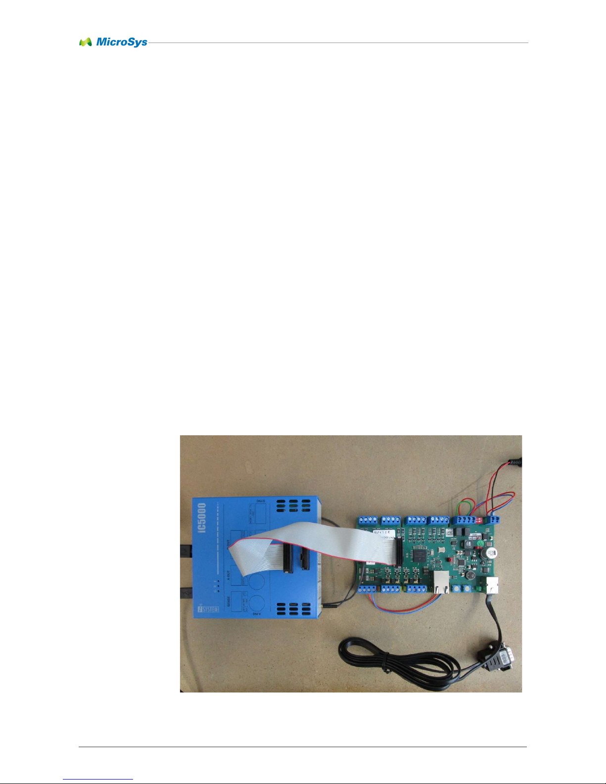
3.3.2 Cabling
Connect the 24V power supply to PWR connector on the rear of board
Make a connection between PWR and PWIN (picture below shows a red
and a blue wire)
Make a loopback connection between the 2 CAN ports (picture below
shows a red and a green wire)
Connect RS232 console cable (included)
Page 12

Quick Start Guide 3
miriac EK
-
5744 User Manual
V 1.2 12/53
© MicroSys Electronics GmbH 2017
3.3.3 Evaluation Software Startup
When power is supplied the system will start automatically.
On startup, the console should show the following output:
The exact output may vary, depending on system and software versions in use. Make
sure to connect the CAN loopback connector and also to connect to a network with
DHCP support.
Welcome to the MPC5744P Ethernet Demo
debug console
PwSBC_IsrSIUL_local
IOinoutStat = 0x00000811
PwSBCDiagVreg2 = 0x00000000
PwSBCDiagVreg3 = 0x00000000
PwSBCStatusVreg2 = 0x00000020
Link established with ETHERPHY
Initalized Stack...
Started DHCP service
Mounted FileSystem
HTTP Server Initiated
Waiting for DHCP server to assign IP...
DHCP assigned IP: 192.168.0.191
WebServer is accessible via web
browser. Use the assigned IP as URL
AIN0 Value = 0x0001
AIN1 Value = 0x0001
AIN2 Value = 0x0001
AIN3 Value = 0x0001
AIN4 Value = 0x0000
AIN5 Value = 0x0000
AIN6 Value = 0x0000
AIN7 Value = 0x0000
pSBC Temp = 29.78
pSBC VREF = 2.5
pSBC VNS_WIDE = 23.1
pSBC IO0_WIDE = 23.1
pSBC IO1_WIDE = 0.0
pSBC VNS_TIGHT = 9.9
pSBC IO0_TIGHT = 9.9
pSBC IO1_TIGHT = 0.0
can_test start
can_test end
…
AIN0 Value = 0x0000
AIN1 Value = 0x0000
AIN2 Value = 0x0000
AIN3 Value = 0x0000
AIN4 Value = 0x0000
AIN5 Value = 0x0000
AIN6 Value = 0x0000
AIN7 Value = 0x0000
pSBC Temp = 29.86
pSBC VREF = 2.5
pSBC VNS_WIDE = 23.1
pSBC IO0_WIDE = 23.1
pSBC IO1_WIDE = 0.0
pSBC VNS_TIGHT = 9.9
pSBC IO0_TIGHT = 9.9
pSBC IO1_TIGHT = 0.0
can_test start
can_test end
…
Page 13
System Description 4
miriac EK
-
5744 User Manual
V 1.2 13/53
© MicroSys Electronics GmbH 2017
4 System Description
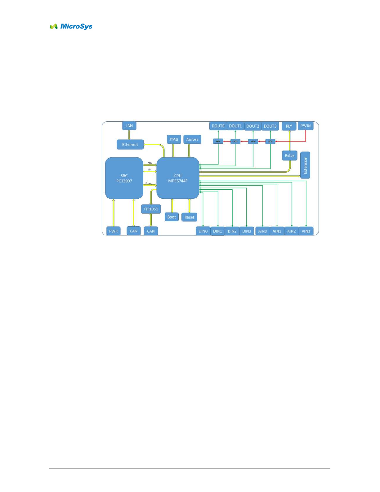
This section describes all parts of the EK-5744 system.
4.1 Block Diagram EK-5744
Page 14
System Description 4
miriac EK
-
5744 User Manual
V 1.2 14/53
© MicroSys Electronics GmbH 2017
4.2 Feature Overview
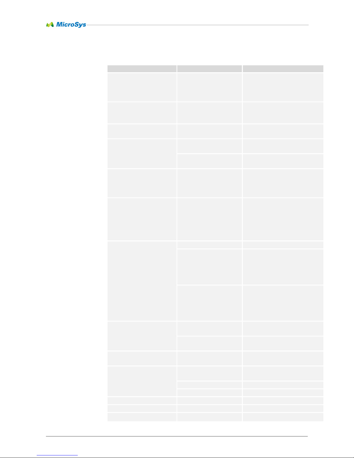
Feature Type Description
CPU NXP MPC5744P
2x Power Architecture e200z4
Core Clock up to 200MHz
384KB RAM (ECC)
2.5MB Flash (ECC)
Ethernet RMII LAN8720A Phy
10/100BaseT
Link / Activity LEDs
Serial Interfaces UART RS232
RJ12 Connector
CAN Interface CAN-1 SBC-PC33907AE
120R Termination
CAN-2 TFJ1051
120R Termination
System Basis Chip PC33907AE Power Conversion
Voltage Supervision
Fail Safe Outputs
High speed CAN interface
Board Switches Push button Switch
Push button Switch
DIP Switch
DIP Switch
2-pin Header
2-pin Header
Power-On Reset
Soft Reset
BMOD Boot Mode
CAN1/2 Termination On/Off
Power Down
Debug
Board Connectors Controller Side 24V Power Input
RJ12 RS232 Port
RJ45 10/100BaseT Port
JTAG Port
Aurora Debug
GPIO Extension Header
IO-Side 24V Power Input
Digital Input 1-4
Digital Output 1-4
Analog Input 1-4
Relay Out
Indicators Controller Side 24V Power Input
3.3V Supply Rail
IO-Side Power Stage Rail
Digital Output 1-4
Debug JTAG
Aurora
14-pin Header
34-pin Connector
Power Supply Controller Side 24V DC @ ??A
Reverse polarity protected
IO-Side 24V DC @ ??A
Reverse polarity protected
Shielding Connector Shield Connected to Ground
Mechanics Dimension ..x..x…mm
Page 15
System Description 4
miriac EK
-
5744 User Manual
V 1.2 15/53
© MicroSys Electronics GmbH 2017
4.3 Mechanical Dimensions
4.3.1 MPX-5744
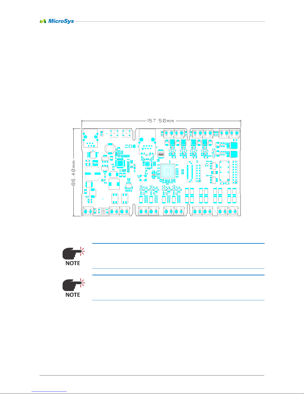
The EK-5744 PCB is suitable for use with an installation component housing of the
BC161 series from © PHOENIX CONTACT. Therefore, there are no mounting
holes on the board. It complies with the standard DIN 43880 for use in common
installation distributor boxes.
This drawing is not to scale.
For 3D data files please contact MicroSys.
Figure 4-1: Mechanical Dimensions
Page 16

System Description 4
miriac EK
-
5744 User Manual
V 1.2 16/53
© MicroSys Electronics GmbH 2017
4.4 Board Layout
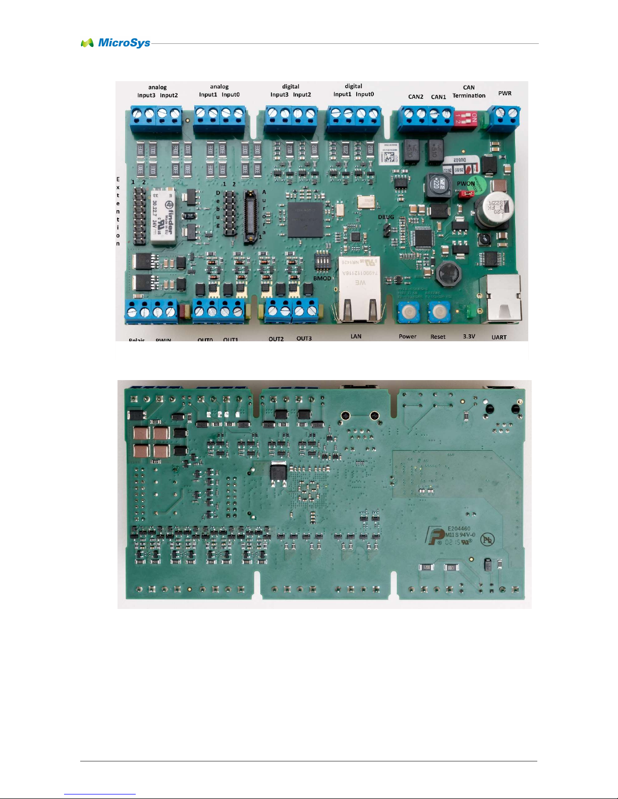
Figure 4-2: Board Layout - Top Side
Page 17
System Description 4
miriac EK
-
5744 User Manual
V 1.2 17/53
© MicroSys Electronics GmbH 2017
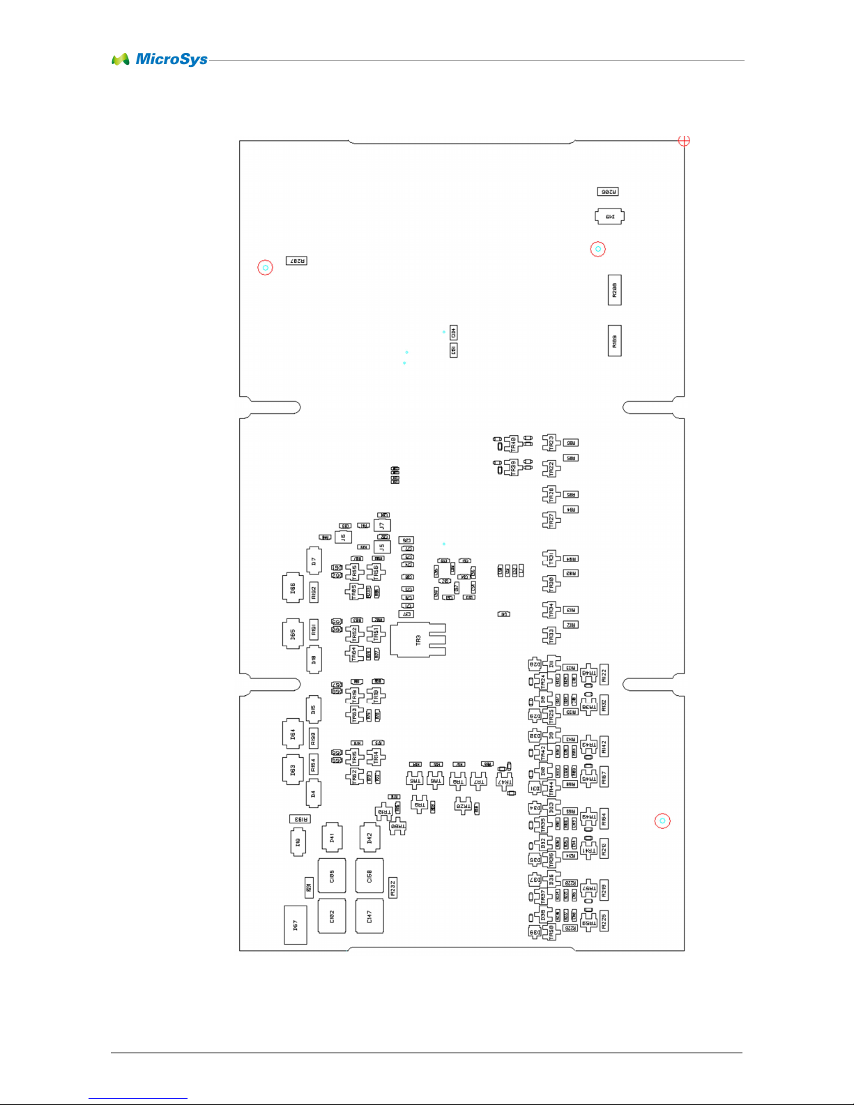
Figure 4-3: Board Layout - Bottom Side
Page 18
System Description 4
miriac EK
-
5744 User Manual
V 1.2 18/53
© MicroSys Electronics GmbH 2017
4.6 Board Views
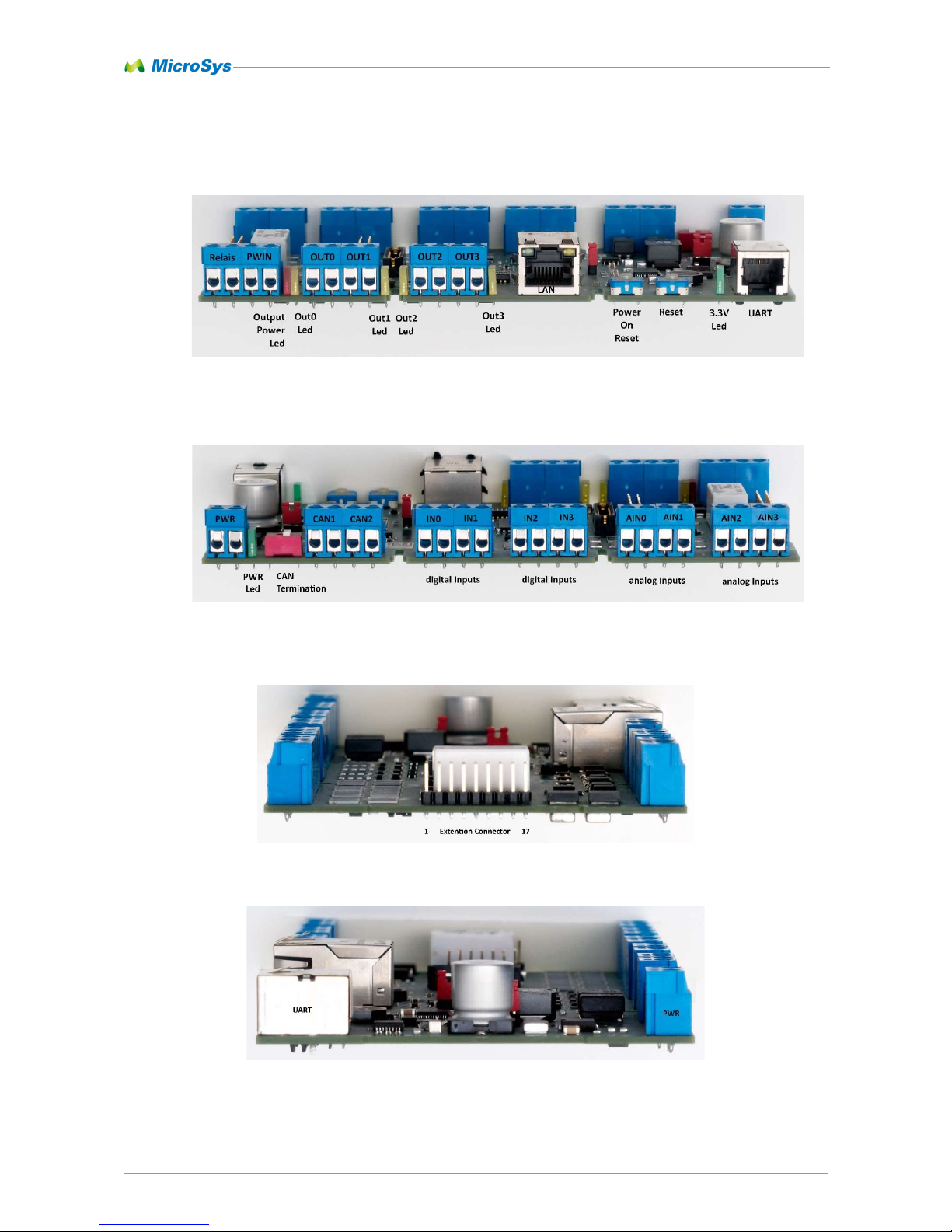
Figure 4-4: Board Front Side View
Figure 4-5: Board Rear View
Figure 4-7: Board Left- Hand Side View
Figure 4-6: Board Right- Hand Side View
Page 19
System Description 4
miriac EK
-
5744 User Manual
V 1.2 19/53
© MicroSys Electronics GmbH 2017
Figure 4-9: Board Top View
Figure 4-8: Board Bottom View
Page 20
System Description 4
miriac EK
-
5744 User Manual
V 1.2 20/53
© MicroSys Electronics GmbH 2017
4.7 System Environment
4.7.1 Temperature Ratings
The EK-5744 contains parts with the following ambient, junction or case
temperature ratings. Due to these limits, the system function is only guaranteed, if
none of them are exceeded at any time.
Part Tmin Tmax
C-0402-XXX-C0G -55°C 125°C
C-0402-XXX-X7R -55°C 125°C
C-0603-XXX-X7R -55°C 125°C
C-0603-XXX-X5R -55°C 85°C
C-0805-XXX-X7R -55°C 125°C
C-0805-XXX-X5R -55°C 85°C
C-1206-XXX-X7R -55°C 125°C
C-1206-XXX-X5R -55°C 85°C
C-1210-XXX-X7R -55°C 125°C
C-1210-XXX-X5R -55°C 125°C
C-2220-XXX-X7R -55°C 125°C
C-EEVFK1J221Q -40°C 105°C
D-1PS70SB20 -55°C 125°C
D-BAS70LT1G -55°C 150°C
D-DDZ9699T -65°C 150°C
D-DFLS240L -55°C 150°C
D-MBRS2H100T3 -65°C 175°C
D-MBRS540 -65°C 125°C
D-MMBD4148 -55°C 150°C
D-PDU540 -65°C 175°C
D-SMAJ12CA -55°C 150°C
D-SUF4005 -50°C 175°C
D-ZMM12 -50°C 175°C
IC-BTS452R -40°C 150°C
IC-LAN8720AI-CP -40°C 85°C
IC-MAX3232EEAE -40°C 85°C
IC-MAX6817EUT -40°C 85°C
IC-MPC5744P_K0MMM5 -40°C 135°C
IC-PC33907AE -40°C 125°C
IC-SN74LVC1G125DCK -40°C 85°C
IC-TJF1051T -40°C 150°C
IC-TL331IDBV -40°C 85°C
L-742-792-040 -55°C 125°C
L-742-792-643 -55°C 125°C
Page 21
System Description 4
miriac EK
-
5744 User Manual
V 1.2 21/53
© MicroSys Electronics GmbH 2017
Part Tmin Tmax
L-742-792-7311 -55°C 125°C
L-744-065-0022 -40°C 125°C
L-744-089-41-010 -40°C 125°C
L-744-227 -40°C 125°C
L-744-7798-221 -40°C 150°C
LD-KBR-L-113GDT -40°C 85°C
LD-KBR-L-113IDT -40°C 85°C
LD-KBR-L-113SYDTK -40°C 85°C
PCB-SBC5744-02 -40°C 85°C
R-0402-XXXX -55°C 125°C
R-0603-XXXX -55°C 125°C
R-0805-XXXX -55°C 125°C
R-1206-XXXX -55°C 125°C
R-2010-XXXX -55°C 155°C
R-2512-XXXX -65°C 170°C
RY-FIN-30.22.7.024 -40°C 850°C
ST-FCI-61885 -40°C 70°C
ST-SAM-ASP-137973-01 -55°C 125°C
ST-WE-691-101-710-002 -40°C 105°C
SW-KNITTER-TSE8S-1 -40°C 85°C
SW-TYCO-1571983-4 -30°C 85°C
SW-WE-418-117-270-902 -40°C 85°C
T-2N7002K -55°C 150°C
T-BC847A -65°C 150°C
T-BCP52 -55°C 150°C
T-BCP56 -65°C 150°C
T-BCR146 -65°C 150°C
T-BSS84P -55°C 150°C
TF-749-901-121-16A -40°C 85°C
T-FMMT493 -55°C 150°C
T-IRLML0100TR -55°C 150°C
T-NDS0605 -55°C 150°C
T-NJD2873T4G -65°C 175°C
T-SI7113DN -50°C 150°C
T-SI7489DP -55°C 150°C
WRAP-2.54-180 -40°C 125°C
XO-FT3B-50.0/100-15/48 -40°C 85°C
XT-FT10A-40MHZ -40°C 85°C
Table 4-1: Component Temperature Ratings
Page 22
System Description 4
miriac EK
-
5744 User Manual
V 1.2 22/53
© MicroSys Electronics GmbH 2017
4.8 Power Supply
4.8.1 Input Supply Rating
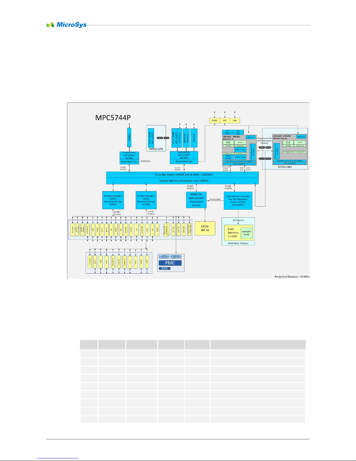
The EK-5744 system is run from two power supplies. One is used for the processor
part, while the second one handles the digital output part of the system.
Both power inputs of the EK-5744 system are protected against wrong polarity and
over-current.
DO NOT exceed the rated maximum values for the power
supply! This may result in severe permanent damage to
the unit, as well as possible serious injury.
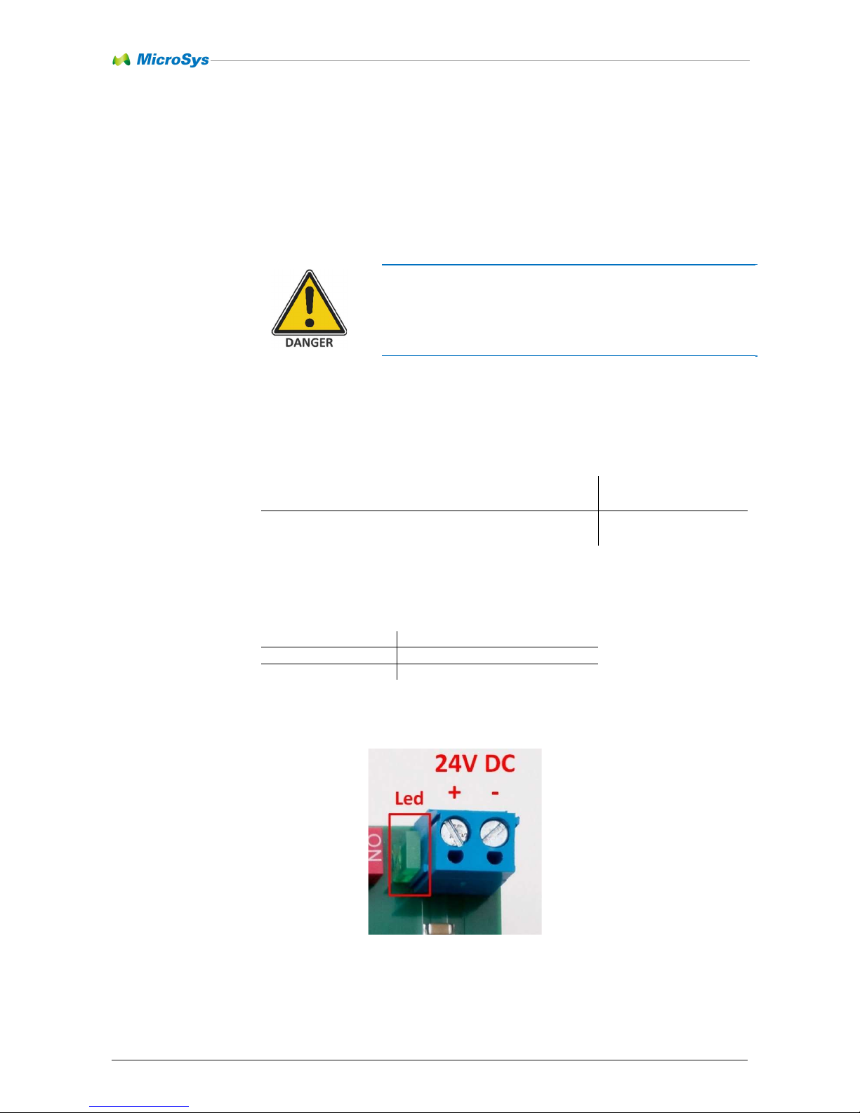
4.8.2 Controller Part Power Connector
The supply should have the following ratings
Input Voltage Operating Range: 24V DC +/-5% 100mA
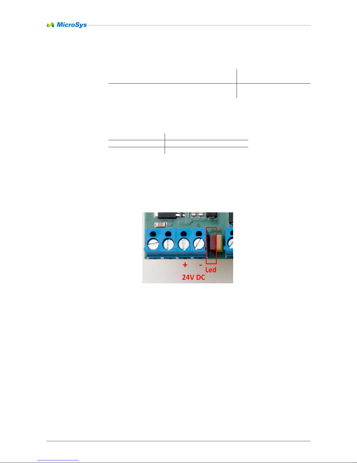
Power is fed to the processor unit via the 2-pin pressure clamp PWR
Manufacturer:
Würth Elektronik
Type:
691-101-710-002
Mates with:
1-2mm² wire
The power is indicated by a green LED beside the connector.
Figure 4-10: Controller Power Part
Connector
Page 23
System Description 4
miriac EK
-
5744 User Manual
V 1.2 23/53
© MicroSys Electronics GmbH 2017
4.8.3 Digital Output Power Connector
The supply should have the following ratings
Input Voltage Operating Range: 24V DC +/-5% min.1A
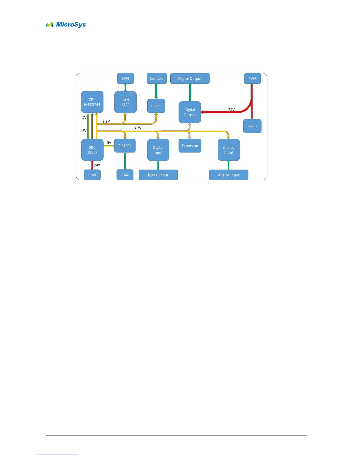
Power is fed to the IO unit via the 2-pin pressure clamp PWIN
Manufacturer:
Würth Elektronik
Type:
691-101-710-002
Mates with:
1-2mm² wire
The red power indicator led is activated only, if one of the two first stage power
switches are on, i.e. if the output drivers for the four digital outputs are supplied
with power.
Figure 4-11: Digital Output Power Connector
(PWIN)
Page 24
System Description 4
miriac EK
-
5744 User Manual
V 1.2 24/53
© MicroSys Electronics GmbH 2017
4.8.4 Power Supply Structure
Figure 4-12 Power supply structure
Page 25
System Core 5
miriac EK
-
5744 User Manual
V 1.2 25/53
© MicroSys Electronics GmbH 2017
5 System Core
5.1 Processor NXP MPC5744
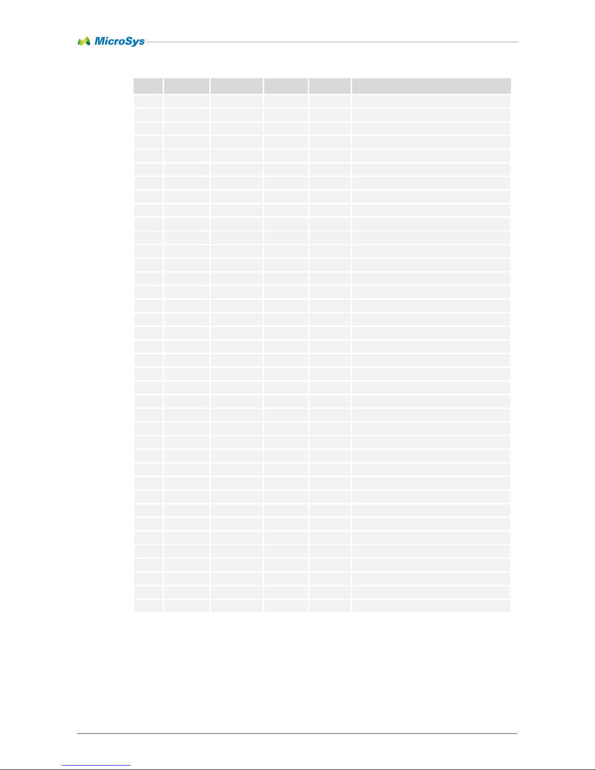
The MPC5744 Qorivva microcontroller is based on an e200 Power Architecture®.
It uses a delayed lock step concept to target the ISO 26262 ASIL-D integrity level.
5.1.1 Processor IO Connections
Pad Signal CPU-I/O Type Active Description
a3 DOUT0
Output
Data high non-inverted output pin state
a5
LDINB#
Output
Stimulus
low global for all digital inputs
a11 DIN0
Input
Data low inverted input pin state
a14 HAIN7#
Output
Stimulus
low unique for this analog input
b4
LDINA#
Output
Stimulus
low global for
all digital inputs
b12 LAIN#
Output
Stimulus
low global for all analog inputs
b13 DIN2
Input
Data low inverted input pin state
b14 PWENA
# Output
Enable
low first stage switch
-
I enable A
b15 DPWSTD
Input
Status
low first stage switch
-
II redundant status
Figure 5-1:Processor Block diagram
Page 26
System Core 5
miriac EK
-
5744 User Manual
V 1.2 26/53
© MicroSys Electronics GmbH 2017
Pad Signal CPU-I/O Type Active Description
c1 DPWSTA
Input
Status
low first stage switch
-
I status
c2
DPWSTC
Input
Status
low first stage switch
-
II status
c6
PWENC
# Output
Enable
low first stage switch
-
II enable C
c7
HAIN4#
Output
Stimulus
low unique for this analog input
c9
DIN1
Input
Data low inverted input pin state
c10 HAIN3#
Output
Stimulus
low unique for this analog input
c11 DPWSTB
Input
Status
low first stage switch
-
I redundant status
d7
DOUT2
Output
Data high non-inverted output pin state
d11 PWEND
# Output
Enable
low first stage
switch
-
II enable D
e15 PWENB
# Output
Enable
low first stage switch
-
I enable B
f17 HAIN5#
Output
Stimulus
low unique for this analog input
g17 HAIN6#
Output
Stimulus
low unique for this analog input
k4
HDIN0#
Output
Stimulus
low unique for this digital
input
l1
DOUT1
Output
Data high non-inverted output pin state
l3
HAIN2#
Output
Stimulus
low unique for this analog input
m3
HDIN2#
Output
Stimulus
low unique for this digital input
m15 HAIN1#
Output
Stimulus
low unique for this analog input
n15 HDIN3#
Output
Stimulus
low unique for this digital input
p5 HDIN1#
Output
Stimulus
low unique for this digital input
p7 AIN5
Input
ADC analog
formated to 3.3V
p8
AIN7
Input
ADC analog
formated to 3.3V
p11 DOSTA0
Input
Status
low output switch 0 status
p17 DIN3
Input
Data low inverted input pin state
r5
AIN1
Input
ADC analog
formated to 3.3V
r6
AIN3
Input
ADC analog
formated to 3.3V
r10 DOSTA1
Input
Status
low output switch 1 status
r11 DOSTA2
Input
Status
low output switch 2 status
r12 DOSTA3
Input
Status
low output switch 3 status
r16 DOUT0
Output
Data high non-inverted output pin state
t5
DOSTB2
Input
Status
low output switch 2 redundant status
t6
DOSTB3
Input
Status
low output switch 3 redundant status
t8
AIN4
Input
ADC analog
formated to 3.3V
t11 AIN6
Input
ADC analog
formated to 3.3V
u3
HAIN0#
Output
Stimulus
low unique for this analog input
u4
DOSTB1
Input
Status
low output switch 1 redundant status
u6
DOSTB0
Input
Status
low output switch 0 redundant status
u7
AIN0
Input
ADC analog
formated to 3.3V
u10 AIN2
Input
ADC analog
formated to 3.3V
Table 5-1: MCU Pin Mapping – Full Overview
Page 27
System Core 5
miriac EK
-
5744 User Manual
V 1.2 27/53
© MicroSys Electronics GmbH 2017
5.1.2 All Processor IO Connections
Pad Signal
Pad Signal
Pad Signal
a3 DOUT0
e15 PWENB
# n3
SBC-LTXD
a4
GPIO9
e17 GPIO62
n14 RMII-CLK a5 LDINB#
f2 RMII-MDIO
n15 HDIN3#
a6
JCOMP
f14 GPIO46
p2 RESET#
a10 MINT#
f15 SBC-LRXD
p3 RMII-RXD0
a11 DIN0
f17 HAIN5#
p5 HDIN1#
a13 CAN2
-
RXD g3
SBC-IO4 p7
AIN5
a14 HAIN7#
g4 SBC-MOSI
p8 AIN7
a15 GPIO93
g14 JTDO
p11 DOSTA0
b4
LDINA#
g15 RGM
-
ABS2
p12 GPIO0
b5
USER
g17 HAIN6#
p14 RMII-TXD0
b6
RMII-MDCK
h1 SBC-MISO
p16 GPIO43
b12 LAIN#
h4 SBC-CS#
p17 DIN3
b13 DIN2
h14 AU-TX0P
r2 SBC-IO2 b14 PWENA
#
h15 JTMS
r4 RMII-RXDV
b15 DPWSTD
h17 JTCK r5
AIN1
c1
DPWSTA
j14 AU-TX0N
r6 AIN3
c2
DPWSTC
j15 AU-CLKN
r10 DOSTA1
c4
SBC-IO3
j17 JTDI
r11 DOSTA2
c5
GPIO13
k1 JNRDY#
r12 DOSTA3
c6
PWENC
# k2
JNEVTO
r16 DOUT0
c7
HAIN4#
k4 HDIN0#
r17 RMII-TXD1
c9
DIN1
k14 AU-TX1N
t3 RMII-RXER
c10 HAIN3#
k15 AU-CLKP
t5 DOSTB2
c11 DPWSTB
k17 AU-RX0P
t6 DOSTB3
c12 MINT#
l1 DOUT1
t8 AIN4
c16 SBC-CTXD
l2 JNEVTI
t11 AIN6
d1
SBC-SCK l3
HAIN2#
t13 SBC-MUXO
d2
GPIO135
l4 MCU
-
FS0
t14 GPIO1
d3
SBC-CRXD
l14 RGM
-
ABS1
t15 GPIO107
d4
SBC-IO5
l15 AU-TX1P
u3 HAIN0#
d6
PORST#
l17 AU-RX0N
u4 DOSTB1
d7
DOUT2
m3 HDIN2#
u6 DOSTB0
d11 PWEND
# m4
RMII-RXD1
u7 AIN0
d12 CAN2
-
TXD
m14 GPIO44
u10 AIN2
d16 RGM
-
FAB
m15 HAIN1#
e4 SBC-INT#
m17 RMII-TXEN
Table 5-2: MCU Pin Mapping – Short Overview
Page 28
System Core 5
miriac EK
-
5744 User Manual
V 1.2 28/53
© MicroSys Electronics GmbH 2017
5.2 LEDs
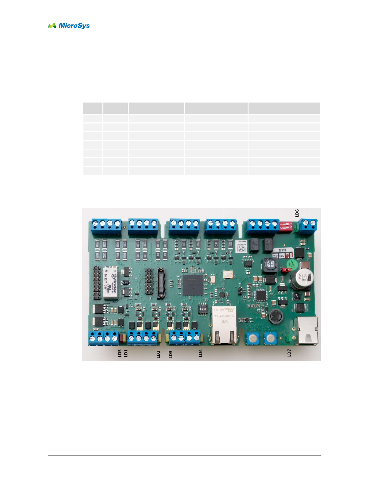
There are seven LEDs onboard the EK-5744. Two LEDs are used to indicate the
power state of the system and five LEDs are used for the digital output part.
LED Color ON OFF Description
LD1 yellow output 0 active output 0 inactive digital output driver state
LD2 yellow output 1 active output 1 inactive digital output driver state
LD3 yellow output 2 active output 2 inactive
digital output driver state
LD4 yellow output 3 active output 3 inactive digital output driver state
LD5 red output supply active output supply inactive digital output driver supply state
LD6 green controller supply active controller supply inactive controller supply state
LD7 green +3.3V supply active +3.3V supply inactive CPU supply state
Table 5-3: LED Pin Mapping
Figure 5-3: MPX-LEDs
Figure 5-2: LED Location and Numbering
Page 29
System Core 5
miriac EK
-
5744 User Manual
V 1.2 29/53
© MicroSys Electronics GmbH 2017
5.3 Switches
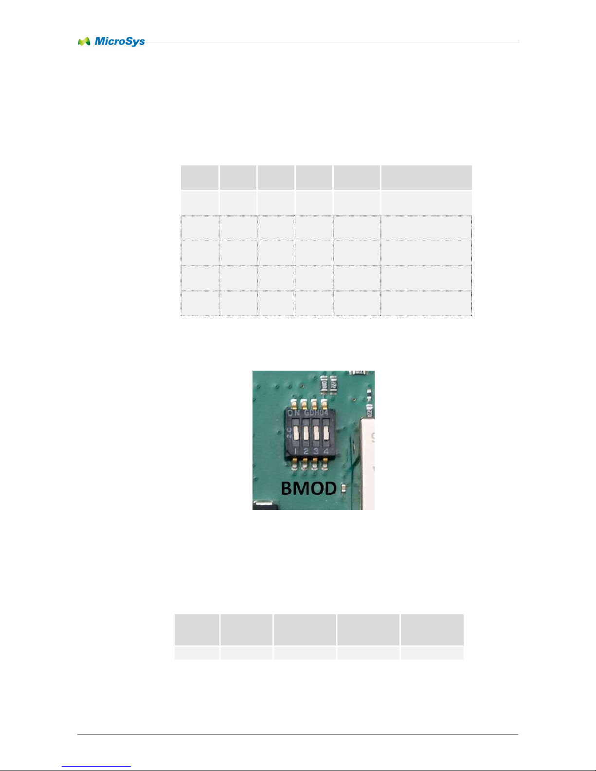
The MPC5744P can handle alternate boot modes, which can be selected by the
DIP switch BMOD according to the following table:
FAB ABS1 ABS0 USER Boot ID Mode
SW1 SW2 SW3 SW4
OFF ON ON --- --- Serial Boot SCI
OFF ON OFF --- --- Serial Boot CAN
ON --- --- --- Valid Single Chip
ON --- --- --- Not found Static Mode
Table 5-4: Boot Modes
Switch 4 of the DIP switch is intended for USER purposes. It is connected to the
MPC5744P processor port B6. If the switch is ON, a logical low will be read back.
CPU
Pad Signal
CPU
Port
SW4
ON
SW4
OFF
b5 USER
B6
LOW
HIGH
Figure 5-4: Boot Mode Switch
Page 30
System Core 5
miriac EK
-
5744 User Manual
V 1.2 30/53
© MicroSys Electronics GmbH 2017
5.4 Jumpers
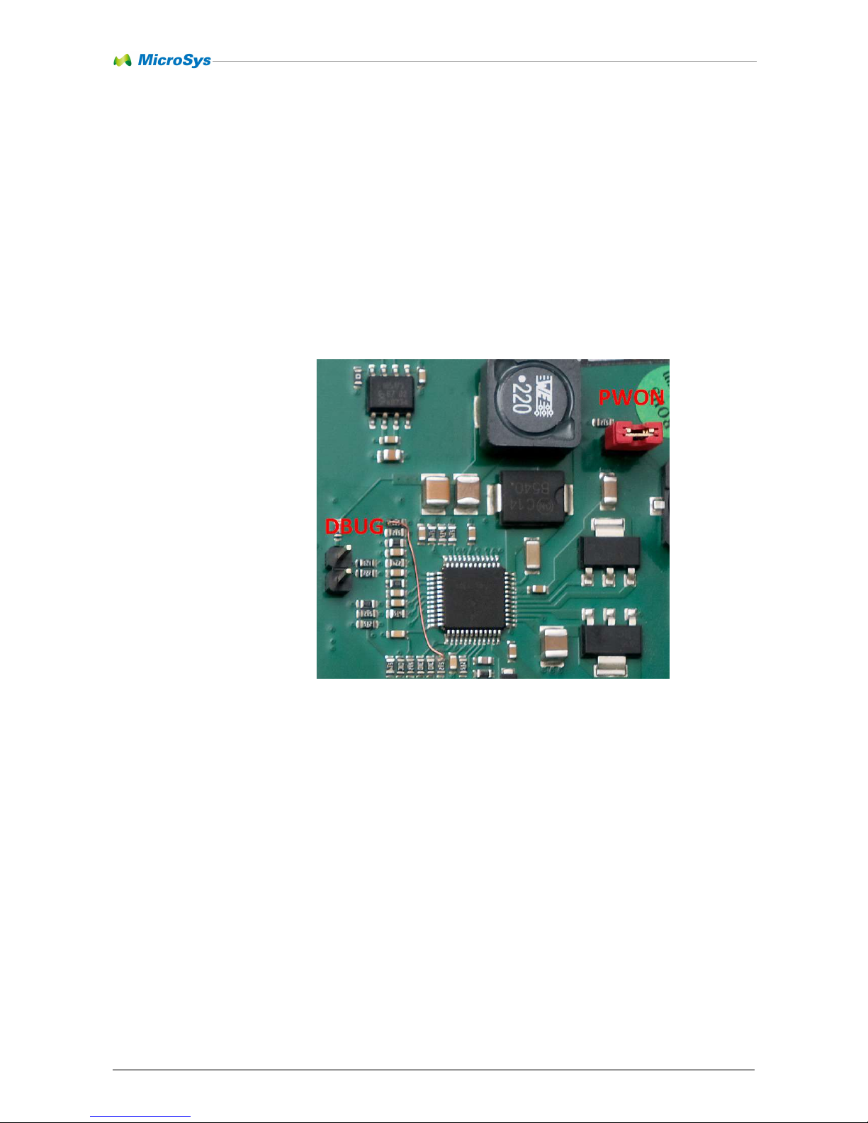
There are two jumpers on the SBC5744. The jumper PWON connects the input
IO_0 of the MC33907 power controller to its input voltage to activate the SBC.
The jumper DBUG is used to enter the Debug mode of the SBC. In Debug mode,
any errors from the watchdog are ignored. If the jumper DBUG is not installed, the
FSI/DEBUG pin of the MC33907 is tied to ground.
Figure 5-5: SBC Jumpers
Page 31
Interfaces 6
miriac EK
-
5744 User Manual
V 1.2 31/53
© MicroSys Electronics GmbH 2017
6 Interfaces
6.1 JTAG and Aurora
6.1.1 JTAG Devices
The JTAG chain of the EK-5744 includes the MPC5744P processor only. The
JTAG port is directly connected to the connector “JTAG” and the Aurora interface
on connector DBG.
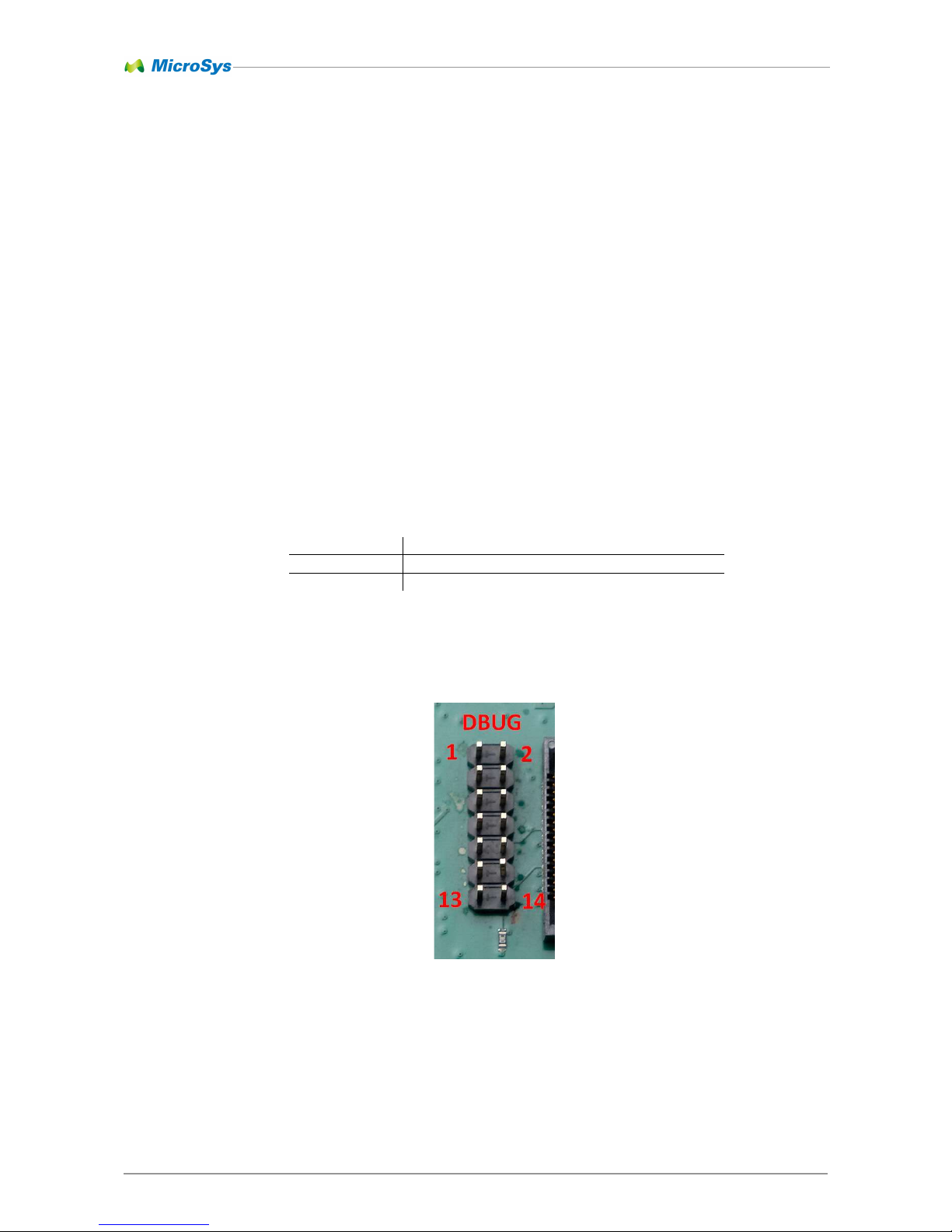
6.1.2 JTAG Connector
The JTAG connector provides all standard JTAG signals for an ARM interface on a
2x5 pin header. Pin 7 of this header usually connects the return clock RTCK and is
not used on the EK-5744. For boundary scan purposes, it can be used to control
the TRST# signal. As this feature is not standard due to the 10-pin ARM interface,
it can be disconnected by the header JRS. The header JRS is located directly behind the reset push button.
Table 6-1 JTAG Header
Manufacturer:
Würth, 61301421121
Type:
2x7 Pin Header, 2.54mm Pitch
Mates with:
Würth, 61201425821
Figure 6-1: JTAG Connector
Page 32
Interfaces 6
miriac EK
-
5744 User Manual
V 1.2 32/53
© MicroSys Electronics GmbH 2017
6.1.3 JTAG Connector Pinout
JTAG MPC5744P I/O
Level
Description
Pin Signal Pin Name Direction Termination
1 JTDI J17 Port B5 LVTTL Input
2 GND
3 JTDO G14 Port B4 LVTTL
Output
4 GND
5 JTCK H17 TCK LVTTL
Input
6 GND
7 JNEVTI L2 Port F11 LVTTL
Input
8 PORST# D6 EXT_POR_B LVTTL
IO 10K Pullup
9 RESET# P2 RESET_B LVTTL
IO 10K Pullup
10 JTMS H15 TMS LVTTL
Input
11 +3.3V
Output
12 GND
13 JNRDY# K1 Port J9 LVTTL
14 JCOMP A6 JCOMP LVTTL
Input 10K Pulldown
Table 6-2: JTAG Connector Pin Mapping
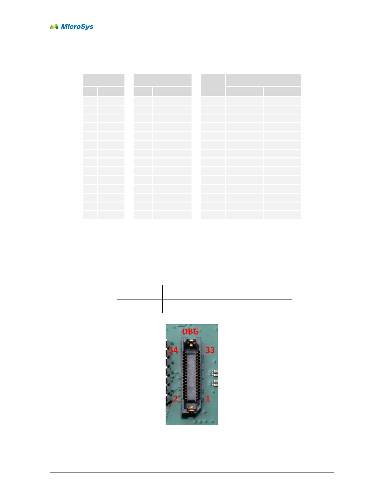
6.1.4 Aurora Connector
The Aurora debug interface is realized as HS34 according to the Nexus 5001
standard with a 34-pin connector.
.
Manufacturer:
Samtec, ASP-137973-01
Type:
2x17 Pin ERM8/ERF8 Edge Rate Connector
Mates with:
Samtec, HDR-142118-XX
Figure 6-2: Aurora Connector
Page 33
Interfaces 6
miriac EK
-
5744 User Manual
V 1.2 33/53
© MicroSys Electronics GmbH 2017
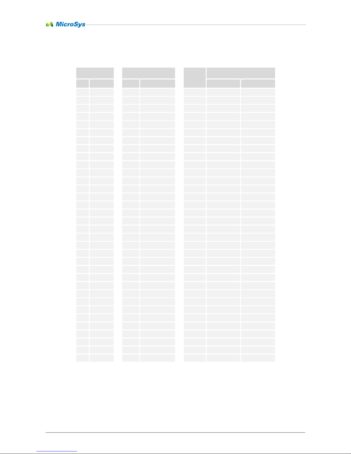
6.1.5 Aurora Connector Pinout
HS34 MPC5744P I/O
Level
Description
Pin Signal Pin Name Direction Termination
1 AU-TX0P H14 Port G12 LVDS Output
2 +3.3V
Output
3 AU-TX0N J14 Port G13 LVDS
Output
4 JTCK H17 TCK LVTTL
Input
5 GND
6 JTMS H15 TMS LVTTL
Input
7 AU-TX1P L15 Port G14 LVDS
Output
8 JTDI J17 Port B5 LVTTL Input
9 AU-TX1N K14 Port G15 LVDS
Output
10 JTDO G14 Port B4 LVTTL
Output
11 GND
Output
12 JCOMP A6 JCOMP LVTTL
Input 10K Pulldown
13 n.c.
14 n.c.
15 n.c.
16 JNEVTI L2 Port F11 LVTTL
Input
17 GND
18 JNEVTO K2 Port F10 LVTTL
Output
19 n.c.
20 PORST# D6 EXT_POR_B LVTTL
IO 10K Pullup
21 n.c.
22 RESET# P2 RESET_B LVTTL
IO 10K Pullup
23 GND
24 GND
25 n.c.
26 AU-CLKP K15 Port H0 LVDS Input
27 n.c.
28 AU-CLKN J15 Port H1 LVDS Input
29 GND
30 GND
31 AU-RX0P K17 Port J10 LVDS Input
32 JNRDY# K1 Port J9 LVTTL
33 AU-RX0N L17 Port J11 LVDS Input
34 n.c.
Table 6-3: Aurora Pin Mapping
Page 34
Interfaces 6
miriac EK
-
5744 User Manual
V 1.2 34/53
© MicroSys Electronics GmbH 2017
6.2 UART
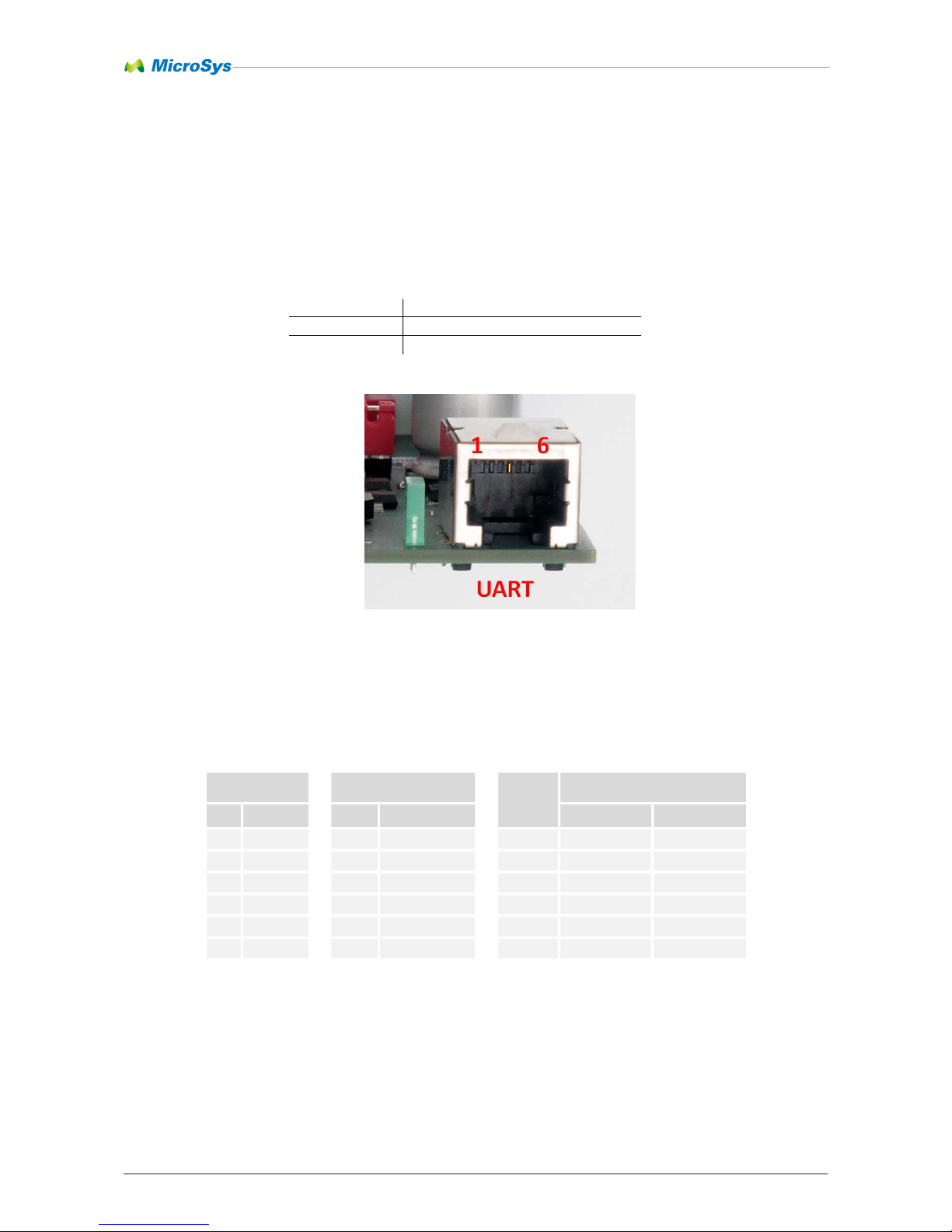
The EK-5744 system provides an RS232 UART interface on the connector LIN.
This two-wire serial connection works with 115200 Baud and no flow control.
6.2.1 RJ11 Connector LIN
Manufacturer:
FCI
Type:
61885
Mates with:
Standard RJ11 jack
6.2.2 LIN Connector Pinout
JTAG MPC5744P I/O
Level
Description
Pin Signal Pin Name Direction Termination
1 n.c.
2 GND
3 TXD N3 Port D9
RS232
Output
4 RXD F15 Port D12
RS232
Input 5K internal
5 n.c.
6 n.c.
Table 6-4: Serial Interface Port Mapping
Figure 6-3: RS232 Connector
Page 35
Interfaces 6
miriac EK
-
5744 User Manual
V 1.2 35/53
© MicroSys Electronics GmbH 2017
6.3 Ethernet
The LAN interface of the EK-5744 uses the 10/100BaseT transceiver LAN8720A.
Its RMII interface incorporates the following lines.
CPU
Pad
Signal
CPU
Port
Description
m4 RMII-RXD1
D5
receive data 1
p3
RMII-RXD0
D6
receive data 0
r4
RMII-RXDV
D7
receive data valid
t3
RMII-RXER
I1
receive error
a10 MINT#
I3
interrupt
b6
RMII-MDCK
F0
management clock
f2
RMII-MDIO
H7
management data
m17 RMII-TXEN
G5
transmit enable
n14 RMII-CLK G8 50MHz
clock
p14 RMII-TXD0
G9
transmit data 0
r17 RMII-TXD1
G10 transmit data 1
Table 6-5: Ethernet Port Pin Mapping
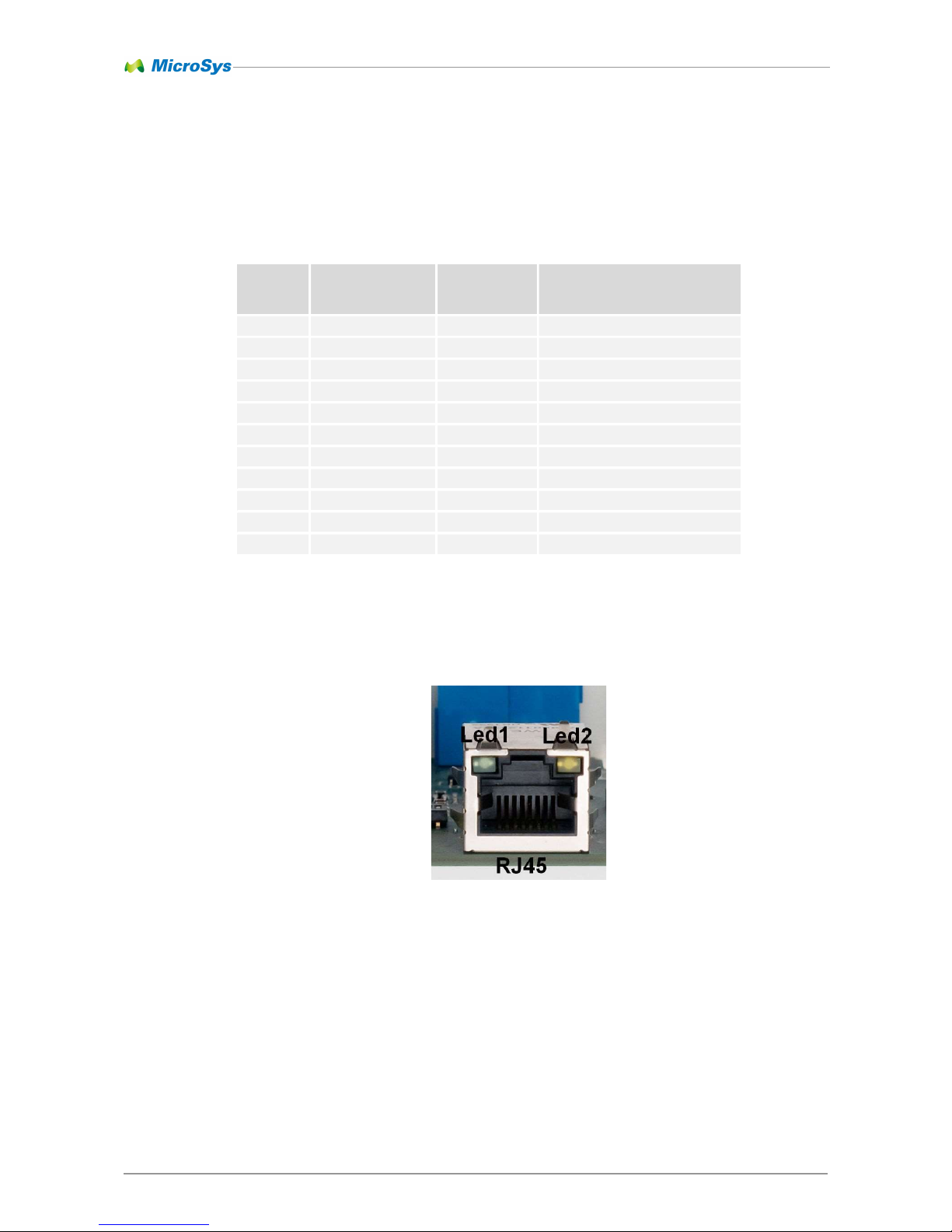
The 10/100BaseT connection is accessible via a standard RJ45 port with
two LEDs, contained within the jack.
LED1 indicates a valid link. LED2 is illuminated at 100Mbps link speed.
Figure 6-4: Ethernet Connector
Page 36
Interfaces 6
miriac EK
-
5744 User Manual
V 1.2 36/53
© MicroSys Electronics GmbH 2017
6.4 CAN
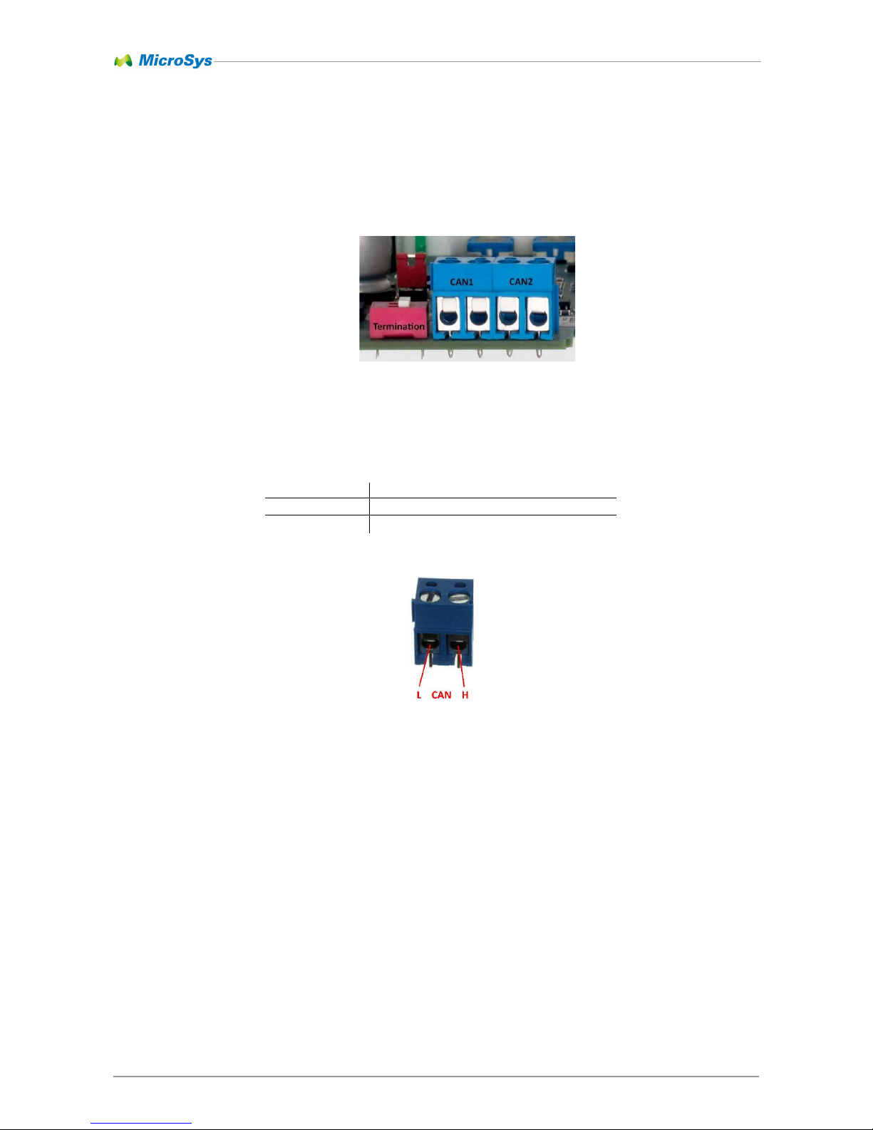
The EK-5744 system offers two CAN interfaces. CAN1 and CAN2 are accessible
via two 2-terminal wire connectors. The necessary 120 Ohm end-point termination
can be activated by two DIP switches.
6.4.1 CAN Connector Block
Manufacturer:
Würth Elektronik
Type:
691 101 710 002
Mates with:
0.13-2.0mm² wire
Figure 6-6: CAN
Terminal Block
Figure 6-5: CAN Connectors
Page 37
Interfaces 6
miriac EK
-
5744 User Manual
V 1.2 37/5
3
© MicroSys Electronics GmbH 2017
6.4.2 CAN Termination
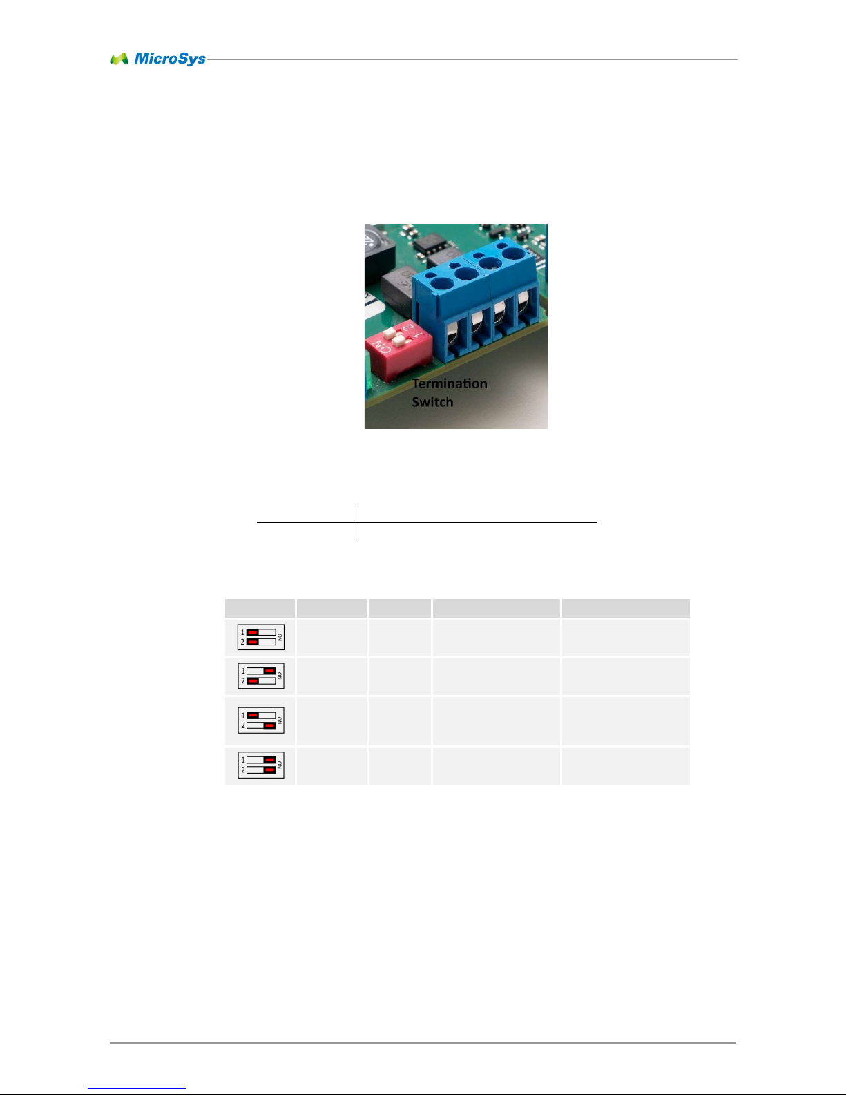
The 120R CAN bus termination is located beside the terminal blocks. It is activated
if the corresponding DIP switch is set to ON.
Manufacturer:
Würth Elektronik
Type:
418117270902
Setting TERM-1 TERM-2 CAN1 CAN2
OFF OFF no termination no termination
ON OFF 120R termination no termination
OFF ON no termination 120R termination
ON ON 120R termination 120R termination
Table 6-6: CAN Termination Switch State Table
Figure 6-7: CAN Termination Switch
Page 38

Interfaces 6
miriac EK
-
5744 User Manual
V 1.2 38/53
© MicroSys Electronics GmbH 2017
6.5 Digital Inputs
There are four digital inputs onboard the EK-5744 operating within the voltage
range 0V-24V according to IEC61131-2 table 7. The CPU reflected state is the inverted state of the input signal, i.e. if an input is unpowered, a logical high state will
be read on the cpu side. All inputs are protected against wrong polarity and are
able to withstand voltages up to 100V in any direction. Each input is fully testable
during operation and has the following specifications. A valid input can only be
read by the CPU if all test features of the input are disabled.
6.5.1 Input Port Specification
Digital Input Specification
input impedance 10-15kOhms
open input state cpu pin high
input low state cpu pin high
input high state cpu pin low
input low range voltage 0-9V
input high range voltage 11-24V
input low range current 0mA-1mA
input high range current 1mA-2.5mA
100V inrush current max.10mA
rising edge delay >10us
falling edge delay >15us
input resistor type MELF
selftestable parts all, except input resistor
input state during test any
Table 6-7: Digital Inputs Electrial Specification
Page 39

Interfaces 6
miriac EK
-
5744 User Manual
V 1.2 39/53
© MicroSys Electronics GmbH 2017
6.5.2 Input CPU Connection
For a correct input read sequence, the common stimuli pins for all inputs LDINA#
and LDINB# as well as the pins HDIN0# to HDIN3# for the corresponding inputs 0
to 3 must be actively set to a high level. A settling time of at least 100us must have
elapsed, before a valid read can be performed.
Digital Input MPC5744P
Pin Name
XDIN0 A11 Port E13
XDIN1 C9 Port H11
XDIN2 B13 Port H9
XDIN3 P17 Port D11
Table 6-8: Digital Inputs Pin Mapping
Stimuli MPC5744P
Low active Pin Name
HDIN0# K4 Port I8
HDIN1# P5 Port I12
HDIN2# M3 Port I10
HDIN3# N15 Port I5
LDINA# B4 Port D2
LDINB# A5 Port D3
Table 6-9: Digital Inputs Stimulus Pin Mapping
6.5.3 Input Test Feature
Each input can be fully tested during normal operation. The test will not be
disturbed by any input state or state change within the given nominal input limits.
The test will overwrite the current input information, so the user must take care
about the system functionality during the test sequence.
A valid input state can only be read if all input test stimuli are disabled for this input.
Page 40

Interfaces 6
miriac EK
-
5744 User Manual
V 1.2 40/53
© MicroSys Electronics GmbH 2017
6.6 Digital Outputs
The four digital outputs of the EK-5744 are designed as high side switches in a redundant two-stage technique.
The first power stage consists of two redundant load switches, which provide the
necessary output power for all four output switches.
The second stage is realized by for high side switches, one for each output.
The output state of each output and each stage is indicated by an LED and can be
read back in a redundant way.
The first stage can be tested during normal operation, without disturbing the current
output configuration.
In case a malfunction of one or more outputs is detected, either the according output can be disabled, or, if this is not possible due to a shorted output driver, the
output power for all four switches can be cut off.
To enable one of the first stage switches, stage AB or stage CD, both PWEN lines
must be set to low.
The states of all outputs and first stages are read back inverted, i.e. a low state indicates an active output on the first and second stage.
Before enabling any of the first stage load switches, the first stage output voltage
must be verified to be in an off state, otherwise a system fault has occurred and
none of the outputs must be activated.
This verification of the output state must also be performed on each output ahead
of any other action. As all outputs are high active, no inactive output must be read
back as a low state on the CPU port.
DO NOT short circuit the output pins. Up until hardware
revision 2, the outputs are not fit to survive short circuit
currents at nominal voltage. Shorts at the output pins
may lead to permanent damage of the output stage
drivers.
Page 41

Interfaces 6
miriac EK
-
5744 User Manual
V 1.2 41/53
© MicroSys Electronics GmbH 2017
6.6.1 Output Port Specification
Digital Input Specification
Output Type High Side Switch
Output Impedance 200mOhms
Output Off Type Open/High Impedance
Output Off State CPU Pin Low
Output On State CPU Pin High
Output Off Range Voltage 0-14V
Output On Range Voltage >23V @24V Supply
Output Off Low Range Current 0-14V/<0.1mA
Output Off High Range Current 14-24V/<10mA
Output On Range Current Nominal 0.25A
Turn On Rise Time <25ns
Turn Off Fall Time <100ns @0.25A
Turn On Delay DOUT->XDOUT <100ns
Turn Off Delay DOUT->XDOUT <150ns
Voltage Injection Protection <0-90V
Reverse Voltage Protection Blocking (max.2A)
Led Indicator Off State 0-14V
Led Indicator On State 16-24V
Status Readback Low 15-24V
Status Readback High 0-13V
Table 6-10: Digital Output Electrical Specification
Page 42
Interfaces 6
miriac EK
-
5744 User Manual
V 1.2 42/53
© MicroSys Electronics GmbH 2017
6.6.2 First Stage Specification
The first stage load switches are current limited, short-circuit and over-temperature
protected.
A single first stage switch is able to deliver more than 1A into the four output
drivers, which allows for a specification of 0.25A per output according to IEC611312 table 9.
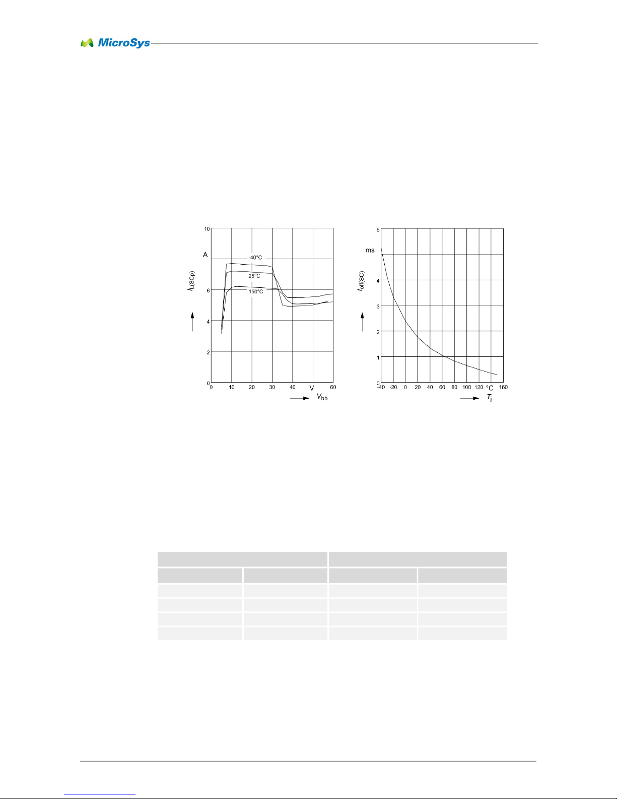
The short current and shutdown time specification of the first stage driver is shown
in the following figure:
The load switch has a delay of 250us which must be taken into account for the
status verification.
For testing the first stage without disturbing active outputs the following sequence
must be performed. We assume that stage AB is active at step 1.
6.6.2.1 First Stage AB/CD Enable
Enable MPC5744P
Signal Stage Pin Name
PWENA#
First Stage AB
B14 Port C10
PWENB#
First Stage AB
E15 Port C13
PWENC#
First Stage CD
C6 Port I0
PWEND#
First Stage CD
D11 Port I2
Table 6-11: Digital Output First Stage Enable Pin Mapping
6.6.2.2 Read Back Status
The read back value of both first stage status lines must be identical.
A low value indicates an active first stage switch.
Figure 6-8: First Stage Switch Timing Specification
Page 43

Interfaces 6
miriac EK
-
5744 User Manual
V 1.2 43/53
© MicroSys Electronics GmbH 2017
Status Ports MPC5744P
Signal Stage Pin Name
DPWSTA
First Stage AB
R16 Port D10
DPWSTB
First Stage AB
C11 Port J2
DPWSTC
First Stage CD
C2 Port J0
DPWSTD
First Stage CD
B15 Port J3
Table 6-12. Digital Output Read Back Pin Mapping
6.6.3 Output Ports
The four ports are powered via the two first stage switches in series with a
protection diode. Each output is driven by a low resistance FET switch in series
with a reverse flow protection diode. These two diodes cause a total voltage drop
of less than 1V between the connector PWIN voltage and an active output.
Each output is fitted with an indicator LED, which will be illuminated at a voltage
greater than 12V at the connector.
A reverse voltage protection diode will short any negative voltage with respect to
ground to eliminate undershots from inductive loads.
There are two redundant status line read-back circuits for each output, which
reflect the real state on the output connector, no matter if the output driver is active
or not.
Above a voltage of 12V at any output port, its status will reflect a logical low. Below
that voltage a logical high will be read back.
Using the status read-back function, an output in an off state can also be used as a
simple input.
The output drivers are realized as a high speed circuit with a turn-on time less than
20ns. The turn-off time depends on the connected load, but can also reach 100ns.
This allows the outputs to be used as PWM drivers without overheating them.
6.6.3.1 CPU Output Ports
Digital Output MPC5744P
Port State Type Pin Name Value
XDOUT0 low inactive R16 Port D10 1
XDOUT0 high active R16 Port D10 0
XDOUT1 low inactive L1 Port H8 1
XDOUT1 high active L1 Port H8 0
XDOUT2 low inactive D7 Port A12 1
XDOUT2 high active D7 Port A12 0
XDOUT3 low inactive A3 Port A15 1
XDOUT3 high active A3 Port A15 0
Table 6-13: Digital Output Pin Mapping
Page 44
Interfaces 6
miriac EK
-
5744 User Manual
V 1.2 44/53
© MicroSys Electronics GmbH 2017
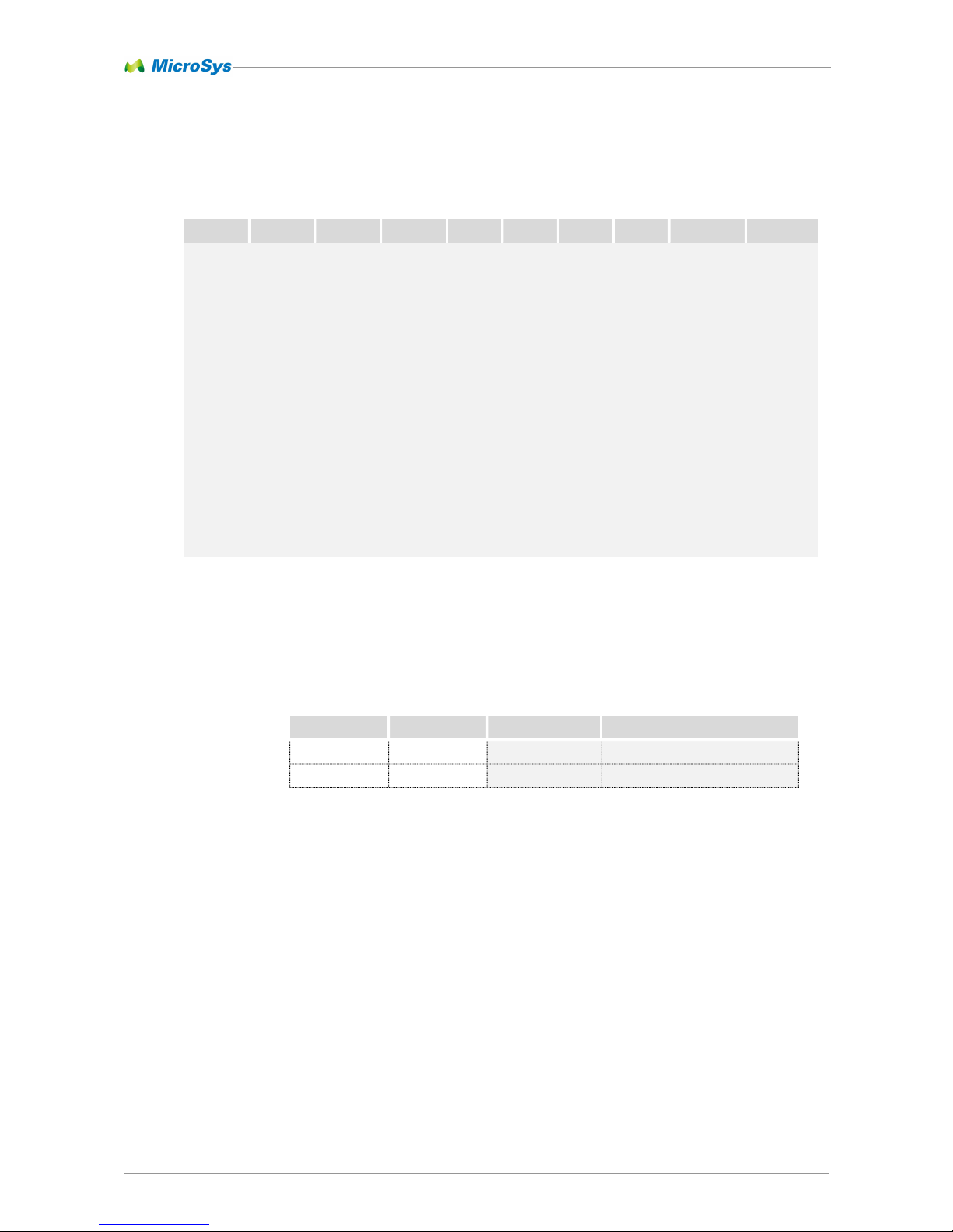
6.6.3.2 Output Truth Table
The “X” denotes this field is not relevant for the current output, however the
corresponding output can be tested to stay inactive in both states of the bit.
PWENA# PWENB# PWENC# PWEND# DOUT0 DOUT1 DOUT2 DOUT3 First Stage Outputs
1 1 1 1 X X X X off all off
0 1 1 1 X X X X off all off
1 0 1 1 X X X X off all off
0 0 1 1 0 0 0 0 on all off
0 0 1 1 1 0 0 0 on Out0 = ON
0 0 1 1 0 1 0 0 on Out1= ON
0 0 1 1 0 0 1 0 on Out2 = ON
0 0 1 1 0 0 0 1 on Out3 = ON
1 1 0 1 X X X X off all off
1 1 1 0 X X X X off all off
1 1 0 0 0 0 0 0 on all off
0 0 0 0 0 0 0 0 on all off
1 1 0 0 1 0 0 0 on Out0 = ON
1 1 0 0 0 1 0 0 on Out1= ON
1 1 0 0 0 0 1 0 on Out2 = ON
1 1 0 0 0 0 0 1 on Out3 = ON
Table 6-14: Digital Output Truth Table
6.6.3.3 Digital Settling Times
The digital output circuitry contains settling times in the first stage unit. For a correct status read-back of the first stage switches, the following settling times must
be observed.
PWENA/B# DPWSTA/B Settling Time Description
1->0 1->0 >200us First Stage Turn On Delay
0->1 0->1 >40ms First Stage Turn Off Delay
Table 6-15: Digital Outputs First Stage Settling Times
Page 45
Interfaces 6
miriac EK
-
5744 User Manual
V 1.2 45/53
© MicroSys Electronics GmbH 2017
6.7 Analog Inputs
The SBC features four analog current sink inputs. Each channel is connected to
two redundant input circuitries and two redundant analog channels of the MPC5744P. The analog circuitry of each input can be stimulated to detect system faults.
For detecting open or shorted sensor lines, the analog ports use the current mode,
which also makes cable lengths uncritical. The complete input range covers 0mA to
24mA, however the valid range uses only 4mA to 20mA. If a value is detected outside the valid range, the sensor and/or the cabling might be faulty.
A valid measurement of the input current is only possible if no stimuli of the input
circuitry are active, i.e. the test signals HAIN0# to HAIN7# as well as LAIN# must
all be at a logical high.
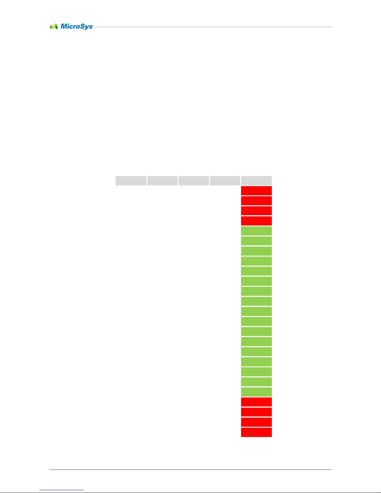
The range of 0-20mA at the connector is translated to an analog voltage of 0V to
2.9V at the MPC5744P port pin according to the following table.
XAINx HAINx# LAIN# AINx Range
0mA high high 0.00V invalid
1mA high high 0.14V invalid
2mA high high 0.29V invalid
3mA high high 0.43V invalid
4mA high high 0.58V valid
5mA high high 0.72V valid
6mA high high 0.87V valid
7mA high high 1.01V valid
8mA high high 1.16V valid
9mA high high 1.30V valid
10mA high high 1.45V valid
11mA high high 1.59V valid
12mA high high 1.74V valid
13mA high high 1.88V valid
14mA high high 2.03V valid
15mA high high 2.17V valid
16mA high high 2.32V valid
17mA high high 2.46V valid
18mA high high 2.61V valid
19mA high high 2.75V valid
20mA high high 2.90V valid
21mA high high 3.04V invalid
22mA high high 3.19V invalid
23mA high high 3.33V invalid
24mA high high 3.48V invalid
Table 6-16: Analog Input 4-20mA Input Validity
Page 46
Interfaces 6
miriac EK
-
5744 User Manual
V 1.2 46/53
© MicroSys Electronics GmbH 2017
6.7.1.1 Analog Port Interconnection
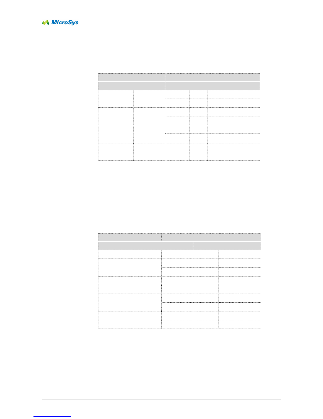
The analog input channles are connected to the analog port of the MPC5744P in
the following manner.
6.7.1.2 Analog Port Stimulation
Each analog input circuitry can be stimulated by two control lines. There is one line
for every channel and one line common for all 8 channels. These lines must be set
inactive during normal operation. An external injected current within the nominal
range will be overwitten by any active stimulus.
Connector MPC-5744P
Name Signal Signal Pad Port
ANI0 XAIN01
AIN0 U7 ADC0_AN0
AIN1 R5 ADC0_ADC1__AN11
ANI1 XANI23
AIN2 U10 ADC1_AN7_ADC3_AN6
AIN3 R6 ADC0_ADC2_AN4
ANI2 XAIN45
AIN4 T8 ADC0_ADC1_AN13
AIN5
P7 ADC0_AN1
ANI3 XANI67
AIN6 T11 ADC1_AN8_ADC3_AN7
AIN7 P8 ADC2_ADC3_AN0
Table 6-17: Analog Input ADC Pin Mapping
Analog MPC-5744P
Input Analog Port Stimulus Pad Port
All Ports AIN0-AIN7 LAIN# B12 B3
XAIN01
AIN0 HAIN0# U3 I11
AIN1 HAIN1# M15 I6
XANI23
AIN2 HAIN2# L3 I9
AIN3 HAIN3# C10 I14
XAIN45
AIN4 HAIN4# C7 H10
AIN5 HAIN5# F17 G2
XANI67
AIN6 HAIN6# G17
G6
AIN7 HAIN7# A14 H13
Table 6-18: Analog Input Stimulus Pin Mapping
Page 47
Interfaces 6
miriac EK
-
5744 User Manual
V 1.2 47/53
© MicroSys Electronics GmbH 2017
6.7.1.3 Analog Stimulation Range
The stimulus function can be used to detect onboard shorts between analog channels. The read back values can be stored and compared over time to detect any
degrading parts. The values may vary from channel to channel due to part tolerances and temperature drift. The influence of an external injected current is below
1mV.
6.7.1.4 Analog Settling Times
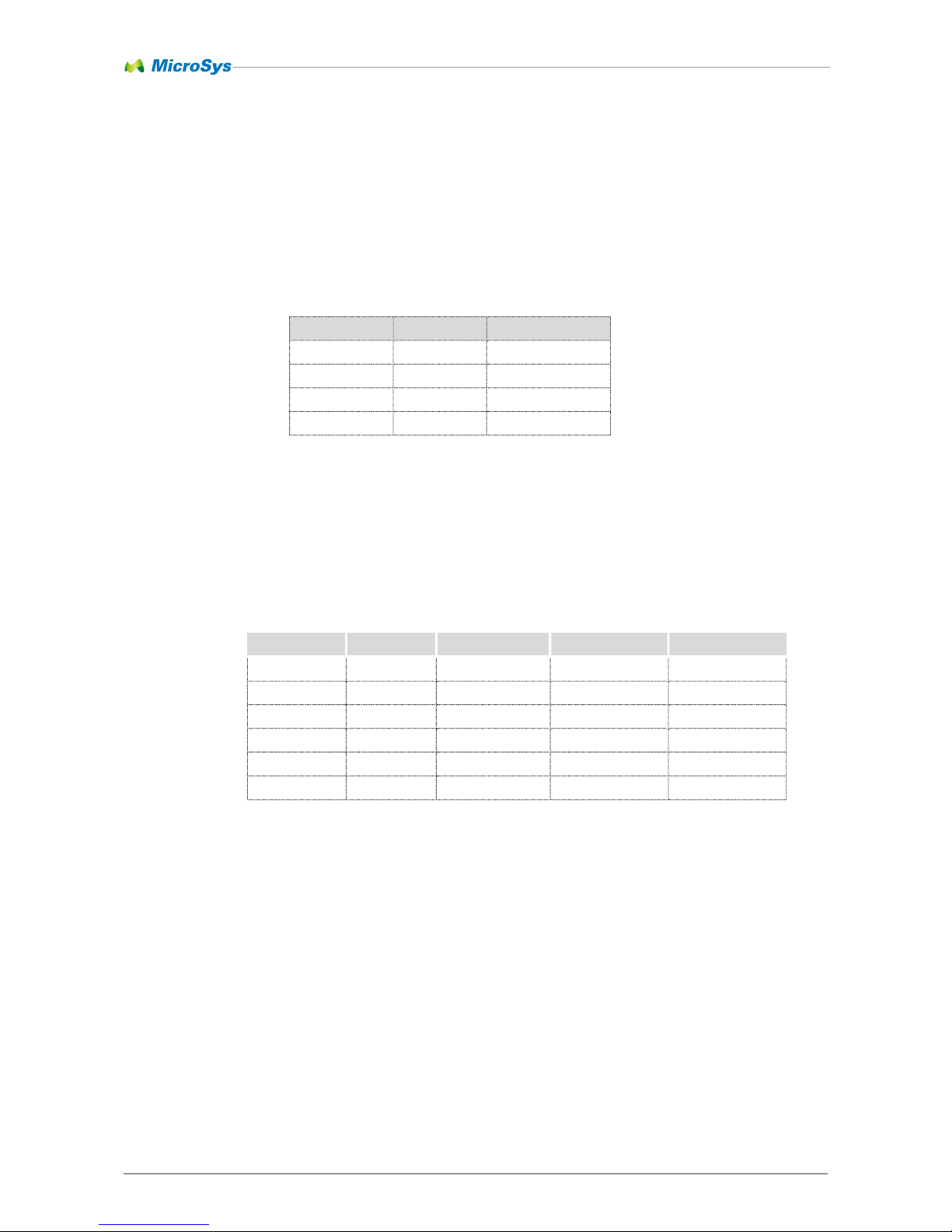
The analog input circuitry is realized with a low pass filter. The settling time of this
filter and the stimuli settling time is described within the following table.
LAIN# HAINx# AINx
1 1 normal operation
0 1 0.0V
0 0 2.99V
1 0 3.24V
Table 6-19: Analog Input Stimulus Ranges
LAIN# HAINx# XAINx AINx Settling Time
1 1 0mA->24mA 100mV->3.5V >250us
1 1 24mA->0mA 3.5V->100mV >2ms
1->0 1 24mA 100mV >400us
0->1 1 24mA 3.5V >250us
1 1->0 0mA 3.2V >50us
0 1->0 0mA 2.95V >50us
Table 6-20: Analog Input Settling Time
Page 48
Interfaces 6
miriac EK
-
5744 User Manual
V 1.2 48/53
© MicroSys Electronics GmbH 2017
6.8 Relay Output
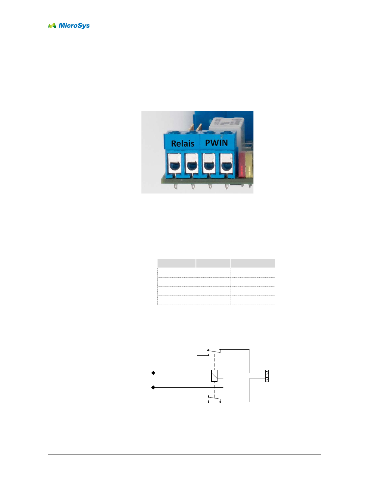
The relay output on the EK-5744 can be accessed via the connector RLY. It is
rated for a maximum switch current of 2A at 30VDC. The save or unpowered state
is open. The switch contacts are isolated with no polarity limitation. It works as well
with AC as with DC voltages.
The relay can only be activated by the SBC and the CPU. Therefore the two lines
MCU-FSO and SBC-FSO# must be set active. The SBC-FSO# is derived from the
MC33907 pin FSOB. The MCU-FSO pin is connected to the MC5744P port D8 on
pad L4.
Basic schematics of the relay in the OFF state.
SBC-FSO# MCU-FSO Relais
0 0 off
0 1 off
1 0 off
1 1 on
Table 6-21: Relay Activation Truth Table
1
21
8
2
3
4
7
6
5
MCU-FS0
SBC-FS0
Figure 6-9: Relay and Digital Output Power Connector
Figure 6-10: Relay operating principle
Page 49
Interfaces 6
miriac EK
-
5744 User Manual
V 1.2 49/53
© MicroSys Electronics GmbH 2017
6.9 Extention Port
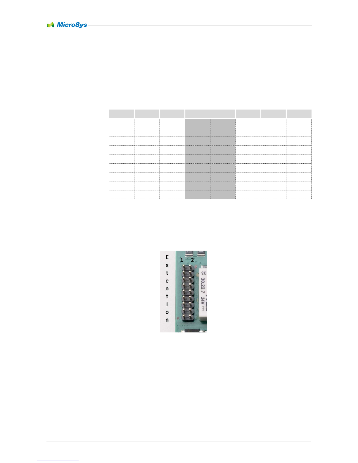
To accommodate some user functions, the extention port on the EK-5744 contains
some 3.3V tolerant CPU pins and a 3.3V supply. All GPIOs are the direct unprotected CPU ports, so care must be taken not to exceed the IO specifications of the
MPC5744P. The 3.3V rail is not able to deliver more than 250mA.
The extention port EXT is realized as an 18-pin header with 2.54mm pitch.
Pad Port Signal EXT Signal Port Pad
+3.3V 1 2 GND
P12 A0 GPIO0 3 4 GPIO1 A1 T14
A4 A9 GPIO9 5 6 GPIO13 A13 C5
n.c. 7 8 n.c.
n.c. 9 10 n.c.
P16 C11 GPIO43 11 12 GPIO44 C12 M14
F14 C14 GPIO46 13 14 GPIO62 D14 E17
A15 F13 GPIO93 15 16 GPIO107 G11 T15
GND 17 18 GPIO135 I7 D2
Table 6-22: Extension Port Connector Pinout Specification
Figure 6-11: Extension Port
Page 50

Appendix 7
miriac EK
-
5744 User Manual
V 1.2 50/53
© MicroSys Electronics GmbH 2017
7 Appendix
7.1 Acronyms
These acronyms are being used within the document; note that this list does not
claim to be complete or exhaustive:
ARM ............................................................................................ Advanced RISC Machine
ESD ................................................................................................ Electrostatic Discharge
GND ........................................................................................................................ Ground
GPIO ................................................................................................... General Purpose IO
GPL ................................................................................................ General Public License
JTAG .............................................................................................. Joint Test Action Group
LED ....................................................................................................... light emitting diode
SBC .................................................................. system basis chip, Single Board Computer
UART .......................................................... Universal Asynchronous Receiver Transmitter
Page 51

Appendix 7
miriac EK
-
5744 User Manual
V 1.2 51/53
© MicroSys Electronics GmbH 2017
7.2 List of Figures
Figure 4-1: Mechanical Dimensions ..................................................................................... 15
Figure 4-2: Board Layout - Top Side .................................................................................... 16
Figure 4-3: Board Layout - Bottom Side ............................................................................... 17
Figure 4-4: Board Front Side View ....................................................................................... 18
Figure 4-5: Board Rear View ................................................................................................ 18
Figure 4-6: Board Right- Hand Side View ............................................................................ 18
Figure 4-7: Board Left- Hand Side View ............................................................................... 18
Figure 4-8: Board Bottom View ............................................................................................ 19
Figure 4-9: Board Top View ................................................................................................. 19
Figure 4-10: Controller Power Part Connector ..................................................................... 22
Figure 4-11: Digital Output Power Connector (PWIN) .......................................................... 23
Figure 4-12 Power supply structure ..................................................................................... 24
Figure 5-1:Processor Block diagram .................................................................................... 25
Figure 5-2: LED Location and Numbering ............................................................................ 28
Figure 5-3: MPX-LEDs ......................................................................................................... 28
Figure 5-4: Boot Mode Switch .............................................................................................. 29
Figure 5-5: SBC Jumpers ..................................................................................................... 30
Figure 6-1: JTAG Connector ................................................................................................ 31
Figure 6-2: Aurora Connector............................................................................................... 32
Figure 6-3: RS232 Connector .............................................................................................. 34
Figure 6-4: Ethernet Connector ............................................................................................ 35
Figure 6-5: CAN Connectors ................................................................................................ 36
Figure 6-6: CAN Terminal Block ........................................................................................... 36
Figure 6-7: CAN Termination Switch .................................................................................... 37
Figure 6-8: First Stage Switch Timing Specification ............................................................. 42
Figure 6-9: Relay and Digital Output Power Connector ....................................................... 48
Figure 6-10: Relay operating principle ................................................................................. 48
Figure 6-11: Extension Port.................................................................................................. 49
Page 52

Appendix 7
miriac EK
-
5744 User Manual
V 1.2 52/53
© MicroSys Electronics GmbH 2017
7.3 List of Tables
Table 1-1 Symbols ................................................................................................................. 5
Table 1-2 Conventions ........................................................................................................... 5
Table 2-1 Safety and Handling Precautions ........................................................................... 6
Table 4-1: Component Temperature Ratings ....................................................................... 21
Table 5-1: MCU Pin Mapping – Full Overview ..................................................................... 26
Table 5-2: MCU Pin Mapping – Short Overview ................................................................... 27
Table 5-3: LED Pin Mapping ................................................................................................ 28
Table 5-4: Boot Modes ......................................................................................................... 29
Table 6-1 JTAG Header ....................................................................................................... 31
Table 6-2: JTAG Connector Pin Mapping ............................................................................ 32
Table 6-3: Aurora Pin Mapping ............................................................................................ 33
Table 6-4: Serial Interface Port Mapping .............................................................................. 34
Table 6-5: Ethernet Port Pin Mapping .................................................................................. 35
Table 6-6: CAN Termination Switch State Table .................................................................. 37
Table 6-7: Digital Inputs Electrial Specification .................................................................... 38
Table 6-8: Digital Inputs Pin Mapping .................................................................................. 39
Table 6-9: Digital Inputs Stimulus Pin Mapping .................................................................... 39
Table 6-10: Digital Output Electrical Specification ................................................................ 41
Table 6-11: Digital Output First Stage Enable Pin Mapping ................................................. 42
Table 6-12. Digital Output Read Back Pin Mapping ............................................................. 43
Table 6-13: Digital Output Pin Mapping ............................................................................... 43
Table 6-14: Digital Output Truth Table ................................................................................. 44
Table 6-15: Digital Outputs First Stage Settling Times ......................................................... 44
Table 6-16: Analog Input 4-20mA Input Validity ................................................................... 45
Table 6-17: Analog Input ADC Pin Mapping ........................................................................ 46
Table 6-18: Analog Input Stimulus Pin Mapping .................................................................. 46
Table 6-19: Analog Input Stimulus Ranges .......................................................................... 47
Table 6-20: Analog Input Settling Time ................................................................................ 47
Table 6-21: Relay Activation Truth Table ............................................................................. 48
Table 6-22: Extension Port Connector Pinout Specification ................................................. 49
Table 8-1 Document history ................................................................................................. 53
Page 53

History 8
miriac EK
-
5744 User Manual
V 1.2 53/53
© MicroSys Electronics GmbH 2017
8 History
Date Version Change Description
2017-07-26 1.0 Initial Release Version (preliminary)
2017-08-01 1.01 MIPI Chapter and Rev 2 photos added
2017-09-01 1.1 Some review inputs implemented. Typos corrected.
Default setting for switches marked.
Preliminary watermark removed.
2017-11-22 1.2 Reworked with respect to design and completeness, added short
circuit warning for outputs
Table 8-1 Document history
 Loading...