

Page 1
micros
®
Systems, Inc.
Workstation 5
Field Service Guide
Copyright 2008, 2009
By MICRO S Systems, Inc.
Colu mbia, Ma r y l a n d USA
All Ri ghts Reserved
Part N umber 100016-166 (2nd Edition)
Page 2

ii
Declarations
Warranties
Although the best efforts are made to ensure that the information
contained in this manua l is complete and correct, MICROS Systems, Inc .
makes no warranty of any kind with r e gard to this material, including but
not limited to the implied warranties of marketability and fitness for a
particular purpose. Information in this manual is subject to change
without notice. MICROS Systems, Inc. shall not be liable for errors
contained here in or for incide ntal or c onsequenti al damages in c onnect ion
with the furnishing, performance, or use of this material.
Trademarks
MICROS is a reg istered trademark of MICROS Systems, Inc.
Microsoft, MS-DOS, Windows, Windows 95, and Windows CE are registered
trademarks of Microsoft Corporation in the U.S. and other countries.
AMD, the AMD logo, and combinations thereof are trademarks of Adva nced
Micro Devices, Inc.
General Software, the GS Logo, Embedded BIOS, CE Ready, the CE Ready
logo, and Firm b ase ar e tradem ark s or re g ister ed tradem ark s of G en e ral
Software, Inc.
Printing History
New editions of this manual incorp orate new and changed material since
the previous edition . Minor co rrections and updates may be incorporated
into reprints of the curr ent edition without changing the date or edition
number.
1st Edition: April 2008
2nd Edition: March, 2009
Page 3

iii
Table Of Content s
Table Of Contents
Preface
Purpo se . . . . . . . . . . . . . . . . . . . . . . . . . . . . . . . . . . . . . . . . . . . . . . . . . . . . . . . .
Who Should Use This Manual? . . . . . . . . . . . . . . . . . . . . . . . . . . . . . . . . vi
Symbo l s . . . . . . . . . . . . . . . . . . . . . . . . . . . . . . . . . . . . . . . . . . . . . . . . . . v i i
Document Design and Production . . . . . . . . . . . . . . . . . . . . . . . . . . . . . . iv
Introd uction to the WS 5 FR U s
Introduction
Casework and Mag Card Reader
Touchs creen Gasket . . . . . . . . . . . . . . . . . . . . . . . . . . . . . . . . . . . . . . . . 1 -3
Top Cov e r . . . . . . . . . . . . . . . . . . . . . . . . . . . . . . . . . . . . . . . . . . . . . . . . 1-3
IO Door . . . . . . . . . . . . . . . . . . . . . . . . . . . . . . . . . . . . . . . . . . . . . . . . . . 1 -4
Workstation 5 B ase . . . . . . . . . . . . . . . . . . . . . . . . . . . . . . . . . . . . . . . . . 1-4
Mag Card Reader Ass e m b l y . . . . . . . . . . . . . . . . . . . . . . . . . . . . . . . . . . 1 -4
Power B u t ton A c t u ator . . . . . . . . . . . . . . . . . . . . . . . . . . . . . . . . . . . . . . 1 -4
System Board and Components
Main Bo a rd , Bare . . . . . . . . . . . . . . . . . . . . . . . . . . . . . . . . . . . . . . . . . . 1-5
USB Flash D ri v e , 4GB . . . . . . . . . . . . . . . . . . . . . . . . . . . . . . . . . . . . . . 1-5
USB Flash Drive, 256M . . . . . . . . . . . . . . . . . . . . . . . . . . . . . . . . . . . . . 1-6
BIOS EE PROM . . . . . . . . . . . . . . . . . . . . . . . . . . . . . . . . . . . . . . . . . . . 1-6
Compact Flash Daughter Card . . . . . . . . . . . . . . . . . . . . . . . . . . . . . . . . 1-6
Compa c t Fla sh Ca r d . . . . . . . . . . . . . . . . . . . . . . . . . . . . . . . . . . . . . . . . 1 -6
DDR333 DIMM . . . . . . . . . . . . . . . . . . . . . . . . . . . . . . . . . . . . . . . . . . . 1-6
Battery, CR2032 . . . . . . . . . . . . . . . . . . . . . . . . . . . . . . . . . . . . . . . . . . . 1-6
Power Supply . . . . . . . . . . . . . . . . . . . . . . . . . . . . . . . . . . . . . . . . . . . . . . . . 1-7
LCD/Touchscreen Assembly
Touchs creen Pan e l . . . . . . . . . . . . . . . . . . . . . . . . . . . . . . . . . . . . . . . . . 1-8
LCD and To u c h screen Bra ck et . . . . . . . . . . . . . . . . . . . . . . . . . . . . . . . . 1-8
LCD Pan e l , 1 5 ” . . . . . . . . . . . . . . . . . . . . . . . . . . . . . . . . . . . . . . . . . . . 1 -8
Backl i g h t In v erter Boar d . . . . . . . . . . . . . . . . . . . . . . . . . . . . . . . . . . . . . 1 -8
Cables
LCD Dat a Ca b l e . . . . . . . . . . . . . . . . . . . . . . . . . . . . . . . . . . . . . . . . . . . 1 -9
Backl i g h t In v erter Boar d Ca b l e . . . . . . . . . . . . . . . . . . . . . . . . . . . . . . . 1-9
Cable Kit , AC Power In - D C Pow e r O u t . . . . . . . . . . . . . . . . . . . . . . 1 -10
Dongle, RJ45-DB9, IDN Port to RS232 2-wire serial . . . . . . . . . . . . . 1-10
Serial Port Conversion Dongle, COM5 RJ45 to DB9 . . . . . . . . . . . . . 1-11
LAN Patch Ca b l es . . . . . . . . . . . . . . . . . . . . . . . . . . . . . . . . . . . . . . . . 1 -11
Cash Drawer Extension Ca b l e s . . . . . . . . . . . . . . . . . . . . . . . . . . . . . . 1-11
Workstation 5 Adjustable Stand Accessories
USB Exten sion Cab l e . . . . . . . . . . . . . . . . . . . . . . . . . . . . . . . . . . . . . . 1 -1 2
Third P a rt y Mo u n t i n g Adapte r . . . . . . . . . . . . . . . . . . . . . . . . . . . . . . . 1-12
Page 4

iv
Table of Contents
LCD Customer Display
LCD Inte r fa ce Board . . . . . . . . . . . . . . . . . . . . . . . . . . . . . . . . . . . . . . 1-13
LCD Module, Optrex . . . . . . . . . . . . . . . . . . . . . . . . . . . . . . . . . . . . . . 1-13
Cable, LCD P o le and Rear Di sp lay Head . . . . . . . . . . . . . . . . . . . . . . 1- 1 4
Cable Exte n sion, LCD Pole Di sp l ay . . . . . . . . . . . . . . . . . . . . . . . . . . 1 - 1 4
LCD Custo mer Display Poles . . . . . . . . . . . . . . . . . . . . . . . . . . . . . . . 1- 1 4
Kit, Front/Rear Cover, /w Lens, Screws, Pole Mount Hinge . . . . . . . 1- 15
Hinge Set , LCD Custom er Displa y . . . . . . . . . . . . . . . . . . . . . . . . . . . 1-15
WS System Board T e ch nical Overview
Worksta t i o n 5 Bl o ck D i a g ram . . . . . . . . . . . . . . . . . . . . . . . . . . . . . . . . . . . 2-2
LX800 Processor and TFT Controller . . . . . . . . . . . . . . . . . . . . . . . . . . . . . 2-4
Processor Core . . . . . . . . . . . . . . . . . . . . . . . . . . . . . . . . . . . . . . . . . . . . 2-5
GeodeL i n k In t e rf a c e Units . . . . . . . . . . . . . . . . . . . . . . . . . . . . . . . . . . . 2-5
GeodeL i n k Me m o ry Co n t roller . . . . . . . . . . . . . . . . . . . . . . . . . . . . . . . 2-6
GeodeL i n k Cont rol Proc essor . . . . . . . . . . . . . . . . . . . . . . . . . . . . . . . . 2 -6
GeodeL i n k In t e rf a ce Block . . . . . . . . . . . . . . . . . . . . . . . . . . . . . . . 2-6
FIFO/Synchronous . . . . . . . . . . . . . . . . . . . . . . . . . . . . . . . . . . . . . . 2-6
Transa c t i o n Forwarding . . . . . . . . . . . . . . . . . . . . . . . . . . . . . . . . . . 2-6
PCI Bus Int e rface Blo c k . . . . . . . . . . . . . . . . . . . . . . . . . . . . . . . . . 2-7
PCI Bus Arb i t e r . . . . . . . . . . . . . . . . . . . . . . . . . . . . . . . . . . . . . . . . 2-7
GeodeL i n k In t e rface General Descript i o n . . . . . . . . . . . . . . . . . . . . 2-7
CS5536 Companion Device . . . . . . . . . . . . . . . . . . . . . . . . . . . . . . . . . . . . . 2-8
System Ma n ag e m e n t Bu s Control l e r . . . . . . . . . . . . . . . . . . . . . . . . . . . 2-8
Serial Interface . . . . . . . . . . . . . . . . . . . . . . . . . . . . . . . . . . . . . . . . . . . . 2-8
Real Time Clock (RTC) and CMO S RA M . . . . . . . . . . . . . . . . . . . . . . 2- 8
ATA Interface . . . . . . . . . . . . . . . . . . . . . . . . . . . . . . . . . . . . . . . . . . . . 2-8
USB Interface . . . . . . . . . . . . . . . . . . . . . . . . . . . . . . . . . . . . . . . . . . . . 2-9
LPC Interface . . . . . . . . . . . . . . . . . . . . . . . . . . . . . . . . . . . . . . . . . . . . . 2-9
Audio Co d e c In t e rface . . . . . . . . . . . . . . . . . . . . . . . . . . . . . . . . . . . . . . 2-9
Divers e Device . . . . . . . . . . . . . . . . . . . . . . . . . . . . . . . . . . . . . . . . . . . . 2-9
Power Ma n a g e m en t Control ler (PMC). . . . . . . . . . . . . . . . . . . . . . . . . 2-10
IDE Interface . . . . . . . . . . . . . . . . . . . . . . . . . . . . . . . . . . . . . . . . . . . . 2-11
TFT LCD an d Ba c k l i g h t In t e rface . . . . . . . . . . . . . . . . . . . . . . . . . . . . . . . 2-1 2
The Grap h i c s P ro c essor (GP) . . . . . . . . . . . . . . . . . . . . . . . . . . . . . . . . 2-12
The Displ ay Co n t roller (DC) . . . . . . . . . . . . . . . . . . . . . . . . . . . . . . . . 2- 1 3
Video Pr o ce ssor (VP ) . . . . . . . . . . . . . . . . . . . . . . . . . . . . . . . . . . . . . 2 - 1 3
LCD Inte rface . . . . . . . . . . . . . . . . . . . . . . . . . . . . . . . . . . . . . . . . . . . 2-14
Backlight Interface . . . . . . . . . . . . . . . . . . . . . . . . . . . . . . . . . . . . . . . . 2-15
Config u rat i o n Ju mpers . . . . . . . . . . . . . . . . . . . . . . . . . . . . . . . . . . 2-15
USB Interface . . . . . . . . . . . . . . . . . . . . . . . . . . . . . . . . . . . . . . . . . . . . . . 2-16
Companion Device . . . . . . . . . . . . . . . . . . . . . . . . . . . . . . . . . . . . . . . 2-16
USB Flash Dr i v e Pow er Contr o ll er . . . . . . . . . . . . . . . . . . . . . . . . 2 -16
CN6 Port Power . . . . . . . . . . . . . . . . . . . . . . . . . . . . . . . . . . . . . . . . . . 2-16
USB Hub . . . . . . . . . . . . . . . . . . . . . . . . . . . . . . . . . . . . . . . . . . . . . . . 2-17
Page 5

v
Table Of Content s
CN8 Por t P o w er . . . . . . . . . . . . . . . . . . . . . . . . . . . . . . . . . . . . . . . . . . 2 -1 8
Touchs creen In t e rf a c e . . . . . . . . . . . . . . . . . . . . . . . . . . . . . . . . . . . . . . . . . 2-19
LPC Inte r face . . . . . . . . . . . . . . . . . . . . . . . . . . . . . . . . . . . . . . . . . . . . . . . 2 -20
AC’97 A u d i o In t e r fa ce . . . . . . . . . . . . . . . . . . . . . . . . . . . . . . . . . . . . . . . . 2-21
Realtek ALC203E . . . . . . . . . . . . . . . . . . . . . . . . . . . . . . . . . . . . . . . . 2-23
Speaker and Lin e Out p u t s . . . . . . . . . . . . . . . . . . . . . . . . . . . . . . . . . . 2-23
Point Of Sale Inte rf a c es. . . . . . . . . . . . . . . . . . . . . . . . . . . . . . . . . . . . . . . . 2 -2 3
Customer Display Interface . . . . . . . . . . . . . . . . . . . . . . . . . . . . . . . . . 2-23
Sendin g D a t a to t h e C u st o m e r Display . . . . . . . . . . . . . . . . . . . . . . 2 -2 3
Receiving Data from the Rear Display . . . . . . . . . . . . . . . . . . . . . . 2-24
Receiving Data from the Pole Display . . . . . . . . . . . . . . . . . . . . . . 2-24
Customer Display VCC Switch . . . . . . . . . . . . . . . . . . . . . . . . . . . 2-2 4
The LCD Customer D i sp l a y . . . . . . . . . . . . . . . . . . . . . . . . . . . . . . 2-2 4
Mag Str i pe Reader Int e rface . . . . . . . . . . . . . . . . . . . . . . . . . . . . . . . . . 2-2 5
IDN Port . . . . . . . . . . . . . . . . . . . . . . . . . . . . . . . . . . . . . . . . . . . . . . . . 2-26
IDN Transmit . . . . . . . . . . . . . . . . . . . . . . . . . . . . . . . . . . . . . . . . . 2-27
IDN Receive . . . . . . . . . . . . . . . . . . . . . . . . . . . . . . . . . . . . . . . . . . 2-27
RS422 Termination . . . . . . . . . . . . . . . . . . . . . . . . . . . . . . . . . . . . 2-27
IDN Port RS232 Interface . . . . . . . . . . . . . . . . . . . . . . . . . . . . . . . . . . 2-28
RS232 Transmit . . . . . . . . . . . . . . . . . . . . . . . . . . . . . . . . . . . . . . . 2-28
RS232 Receive . . . . . . . . . . . . . . . . . . . . . . . . . . . . . . . . . . . . . . . . 2-28
COM5 Modular RS232 Port . . . . . . . . . . . . . . . . . . . . . . . . . . . . . . . . . 2-29
COM1 DB9 Po r t . . . . . . . . . . . . . . . . . . . . . . . . . . . . . . . . . . . . . . . . . . 2-29
Cash Drawer Interface . . . . . . . . . . . . . . . . . . . . . . . . . . . . . . . . . . . . . 2-30
Cash Drawer Clos e d De tection . . . . . . . . . . . . . . . . . . . . . . . . . . . 2-3 0
+24V Regu l ator . . . . . . . . . . . . . . . . . . . . . . . . . . . . . . . . . . . . . . . 2-31
System Bo a rd Hardware Rev is i o n . . . . . . . . . . . . . . . . . . . . . . . . . . . . 2-31
RTL8110SC Ethernet Controller . . . . . . . . . . . . . . . . . . . . . . . . . . . . . . . . 2-32
Genera l D escription . . . . . . . . . . . . . . . . . . . . . . . . . . . . . . . . . . . . . . . 2 -3 2
PCI Bus Interface . . . . . . . . . . . . . . . . . . . . . . . . . . . . . . . . . . . . . . . . . 2-32
Link, Speed and Activity LED Co n t rol . . . . . . . . . . . . . . . . . . . . . . . . 2-32
EEPROM In t e rface . . . . . . . . . . . . . . . . . . . . . . . . . . . . . . . . . . . . . . . . 2-3 3
System Bo a rd Power D i st ributio n . . . . . . . . . . . . . . . . . . . . . . . . . . . . . . . 2-34
Standby Domain Voltages . . . . . . . . . . . . . . . . . . . . . . . . . . . . . . . . . . 2-35
+12V . . . . . . . . . . . . . . . . . . . . . . . . . . . . . . . . . . . . . . . . . . . . . . . . 2 -35
VCC5SB . . . . . . . . . . . . . . . . . . . . . . . . . . . . . . . . . . . . . . . . . . . . . 2 -3 5
VCC3SB . . . . . . . . . . . . . . . . . . . . . . . . . . . . . . . . . . . . . . . . . . . . . 2 -3 5
VCORE SB. . . . . . . . . . . . . . . . . . . . . . . . . . . . . . . . . . . . . . . . . . . . 2-35
VCC1.8S B . . . . . . . . . . . . . . . . . . . . . . . . . . . . . . . . . . . . . . . . . . . 2-35
Workin g Dom a i n V o l t a g e s . . . . . . . . . . . . . . . . . . . . . . . . . . . . . . . . . . 2-36
VCC12 . . . . . . . . . . . . . . . . . . . . . . . . . . . . . . . . . . . . . . . . . . . . . . 2-36
VCC3 . . . . . . . . . . . . . . . . . . . . . . . . . . . . . . . . . . . . . . . . . . . . . . . 2-36
VCC5 . . . . . . . . . . . . . . . . . . . . . . . . . . . . . . . . . . . . . . . . . . . . . . . 2-36
VCC -12 . . . . . . . . . . . . . . . . . . . . . . . . . . . . . . . . . . . . . . . . . . . . . 2-36
VCORE . . . . . . . . . . . . . . . . . . . . . . . . . . . . . . . . . . . . . . . . . . . . . . 2-37
Page 6

vi
Table of Contents
Working, Standby and System Reset . . . . . . . . . . . . . . . . . . . . . . . . . . 2-37
Worksta t i o n 5 Backlight In v e r t e r Board . . . . . . . . . . . . . . . . . . . . . . . . . . 2-38
Functi onal Description . . . . . . . . . . . . . . . . . . . . . . . . . . . . . . . . . . . . . 2-38
Techni c a l De sc r iption . . . . . . . . . . . . . . . . . . . . . . . . . . . . . . . . . . . . . 2-3 8
Supply Monitoring . . . . . . . . . . . . . . . . . . . . . . . . . . . . . . . . . . . . . 2-38
Lamp Strike . . . . . . . . . . . . . . . . . . . . . . . . . . . . . . . . . . . . . . . . . . 2-38
Run Lam p . . . . . . . . . . . . . . . . . . . . . . . . . . . . . . . . . . . . . . . . . . . 2-38
Bright ness Contro l . . . . . . . . . . . . . . . . . . . . . . . . . . . . . . . . . . . . . 2-39
Workstation 5 Troubleshoo tin g
Introduction
Operational Troubleshooting . . . . . . . . . . . . . . . . . . . . . . . . . . . . . . . . . . . . 3-3
Worksta t i o n 5 Boo t Sequen c e . . . . . . . . . . . . . . . . . . . . . . . . . . . . . . . . 3-3
Booting to Windows Embedded CE 6.0 . . . . . . . . . . . . . . . . . . . . . . . . 3-8
Booting to W EP O S . . . . . . . . . . . . . . . . . . . . . . . . . . . . . . . . . . . . . . . 3-10
Background Information . . . . . . . . . . . . . . . . . . . . . . . . . . . . . . . . . . . . . . 3-11
Multiple Boot Configurations . . . . . . . . . . . . . . . . . . . . . . . . . . . . . . . 3-11
Windows Embedded CE 6.0 . . . . . . . . . . . . . . . . . . . . . . . . . . . . . . . . 3- 11
WEPOS . . . . . . . . . . . . . . . . . . . . . . . . . . . . . . . . . . . . . . . . . . . . . . . . 3-11
Pre-boot Firmware Applications . . . . . . . . . . . . . . . . . . . . . . . . . . . . . . . . 3-12
Platform Updates . . . . . . . . . . . . . . . . . . . . . . . . . . . . . . . . . . . . . . . . . 3-12
CAL32 . . . . . . . . . . . . . . . . . . . . . . . . . . . . . . . . . . . . . . . . . . . . . . . . . . . . 3-13
Power- On Self Test (P O ST) Errors . . . . . . . . . . . . . . . . . . . . . . . . . . . . . . 3 -14
Checking the Power Supply and System Board Voltages . . . . . . . . . . . . . 3-15
WS5 System Board - Standby Vo l t a g es . . . . . . . . . . . . . . . . . . . . . . . 3-15
WS5 System Board - Wo rk i n g V o l tages . . . . . . . . . . . . . . . . . . . . . . . 3 -17
Workstation Recovery and Platform Update Procedures
Windows Embedded CE 6.0 . . . . . . . . . . . . . . . . . . . . . . . . . . . . . . . . . . . 3-19
Using WC F . . . . . . . . . . . . . . . . . . . . . . . . . . . . . . . . . . . . . . . . . . . . . 3-19
Using th e CA L t o Configure a Workstati o n . . . . . . . . . . . . . . . . . . . . 3-20
The CAL Download s the POS Appli c at ion . . . . . . . . . . . . . . . . . . . . . 3 -20
Stand-A l o n e CA L . . . . . . . . . . . . . . . . . . . . . . . . . . . . . . . . . . . . . . . . 3- 2 0
Using Windows CE Factory Restore . . . . . . . . . . . . . . . . . . . . . . . . . . . . . 3-21
Factory Re store Pr o ce d u r e . . . . . . . . . . . . . . . . . . . . . . . . . . . . . . . . . . 3-22
WEPOS . . . . . . . . . . . . . . . . . . . . . . . . . . . . . . . . . . . . . . . . . . . . . . . . . . . 3-23
LCD Display Related . . . . . . . . . . . . . . . . . . . . . . . . . . . . . . . . . . . . . . . . . 3-24
Dark LCD (N o Backlight) . . . . . . . . . . . . . . . . . . . . . . . . . . . . . . . . . . 3- 2 4
Blank LC D (No Vid e o ). . . . . . . . . . . . . . . . . . . . . . . . . . . . . . . . . . . . . 3-24
Flickering LCD . . . . . . . . . . . . . . . . . . . . . . . . . . . . . . . . . . . . . . . . . . 3-24
LCD Back l i g h t too D im . . . . . . . . . . . . . . . . . . . . . . . . . . . . . . . . . . . . 3-25
LCD Imag e Pr o b l e m . . . . . . . . . . . . . . . . . . . . . . . . . . . . . . . . . . . . . . 3-25
LCD Quality Problem . . . . . . . . . . . . . . . . . . . . . . . . . . . . . . . . . . . . . 3-25
Config u ri n g the LCD Jump ers . . . . . . . . . . . . . . . . . . . . . . . . . . . . . . . 3-25
Touchscreen Related . . . . . . . . . . . . . . . . . . . . . . . . . . . . . . . . . . . . . . . . . 3-27
Touchscreen Not Responding after the Operating System Starts . . . . 3-27
Page 7

vii
Table Of Content s
Touchscreen Ca lib ration . . . . . . . . . . . . . . . . . . . . . . . . . . . . . . . . . . . . 3-2 7
False To u ch e s . . . . . . . . . . . . . . . . . . . . . . . . . . . . . . . . . . . . . . . . . . . . 3-2 9
Local A rea Networ k . . . . . . . . . . . . . . . . . . . . . . . . . . . . . . . . . . . . . . . . . . 3 -2 9
Workstation 5 Does not Conn e ct t o LA N . . . . . . . . . . . . . . . . . . . . . . 3-29
Workstation 5 Does not Conn e ct t o LA N (Link LED OFF ) . . . . . . . . 3-30
Workstation 5 Does not Conn e ct t o LA N (Link LED ON ). . . . . . . . . . 3 -30
Perip h eral Relat e d . . . . . . . . . . . . . . . . . . . . . . . . . . . . . . . . . . . . . . . . . . . 3-3 1
IDN Port COM4 (RS422) Does Not Function . . . . . . . . . . . . . . . . . . . 3-31
RS232 COM4 Peripheral Device Does not Function . . . . . . . . . . . . . . 3-31
COM5 RS232 Port . . . . . . . . . . . . . . . . . . . . . . . . . . . . . . . . . . . . . . . . 3-32
COM1 RS232 Port . . . . . . . . . . . . . . . . . . . . . . . . . . . . . . . . . . . . . . . . 3-32
Mag Str i pe Reader Int e rface . . . . . . . . . . . . . . . . . . . . . . . . . . . . . . . . . 3-3 2
Customer Display Interface . . . . . . . . . . . . . . . . . . . . . . . . . . . . . . . . . 3-33
WS5 Diagnostic . . . . . . . . . . . . . . . . . . . . . . . . . . . . . . . . . . . . . . . . . . . . . 3-34
Windows Embedded CE 6.0 . . . . . . . . . . . . . . . . . . . . . . . . . . . . . . . . . 3-34
WEPOS . . . . . . . . . . . . . . . . . . . . . . . . . . . . . . . . . . . . . . . . . . . . . . . . . 3-34
Starting the WS5DiagUtility . . . . . . . . . . . . . . . . . . . . . . . . . . . . . 3-34
System Information Screen - Hardware Components . . . . . . . . . . 3-35
Syste m I n fo rmatio n Screen - Platform Fi l e s . . . . . . . . . . . . . . . . . 3-37
Activity Counters, Dump Sys Info and Recovery Image Info . . . . 3-41
WEPOS Sy st em Infor m a t ion Screen . . . . . . . . . . . . . . . . . . . . . . . . . . 3-42
Remove and Replace the Workstation 5 FRUs
Disassembli n g th e Workstation 5 . . . . . . . . . . . . . . . . . . . . . . . . . . . . . . . . . 4-2
Magnet ic Card Rea d er . . . . . . . . . . . . . . . . . . . . . . . . . . . . . . . . . . . . . . . . . 4 -5
The Power Supply . . . . . . . . . . . . . . . . . . . . . . . . . . . . . . . . . . . . . . . . . . . . 4-7
LCD/T o u c h screen Proc edures . . . . . . . . . . . . . . . . . . . . . . . . . . . . . . . . . . . 4-8
Touchs creen . . . . . . . . . . . . . . . . . . . . . . . . . . . . . . . . . . . . . . . . . . . . . 4-10
LCD Pan e l . . . . . . . . . . . . . . . . . . . . . . . . . . . . . . . . . . . . . . . . . . . . . . 4-1 2
Backl i g h t In v erter Boar d . . . . . . . . . . . . . . . . . . . . . . . . . . . . . . . . . . . 4-15
Capacitive Touchscreen Interface Board . . . . . . . . . . . . . . . . . . . . . . . 4-16
The System Board
USB Flash D ri v e . . . . . . . . . . . . . . . . . . . . . . . . . . . . . . . . . . . . . . . . . . 4-19
DDR Mem o ry . . . . . . . . . . . . . . . . . . . . . . . . . . . . . . . . . . . . . . . . . . . . 4-2 0
Approv e d D IMMs . . . . . . . . . . . . . . . . . . . . . . . . . . . . . . . . . . . . . 4-21
BIOS EE PROM . . . . . . . . . . . . . . . . . . . . . . . . . . . . . . . . . . . . . . . . . . 4-22
Mini-P CI Wireless Card . . . . . . . . . . . . . . . . . . . . . . . . . . . . . . . . . . . . 4-2 3
The Inte g rated LCD Cu stomer Display . . . . . . . . . . . . . . . . . . . . . . . . . . . 4-2 4
Reass embling the Wo rk stati o n 5 . . . . . . . . . . . . . . . . . . . . . . . . . . . . . . . . 4 -2 5
Connector and Cable Diagrams
IO Panel Connectors . . . . . . . . . . . . . . . . . . . . . . . . . . . . . . . . . . . . . . . . . . .A-2
10/100 Ethernet Connector . . . . . . . . . . . . . . . . . . . . . . . . . . . . . . . . . . .A-4
RS232 Connector . . . . . . . . . . . . . . . . . . . . . . . . . . . . . . . . . . . . . . . . . .A-4
Cash Drawer 1 and 2 Con n ec t o rs . . . . . . . . . . . . . . . . . . . . . . . . . . . . . .A-5
Page 8

viii
Table of Contents
PS2 Mouse/Keyboard Connectors . . . . . . . . . . . . . . . . . . . . . . . . . . . . A-6
Remote Cust o mer Disp l ay Co n n e ctor . . . . . . . . . . . . . . . . . . . . . . . . . . A-6
System Board Connectors . . . . . . . . . . . . . . . . . . . . . . . . . . . . . . . . . . . . . .A- 7
Magnetic Stripe Interface . . . . . . . . . . . . . . . . . . . . . . . . . . . . . . . . . . . .A-7
Hook-up Cables . . . . . . . . . . . . . . . . . . . . . . . . . . . . . . . . . . . . . . . . . . . . . . A-8
RS232 from the RS422-A and RS422-B Ports . . . . . . . . . . . . . . . . . . .A-8
Ethern et. . . . . . . . . . . . . . . . . . . . . . . . . . . . . . . . . . . . . . . . . . . . . . . . . A-9
8-Pin to 6-Pin Hook-up RS422 Cable (300319-001) . . . . . . . . . . . . . .A-11
Cash Drawe r Extens io n Cab l e . . . . . . . . . . . . . . . . . . . . . . . . . . . . . . A-12
Page 9

Workstation 5 Field Service Guide ix
Preface
In this preface, you’ll find information about this manual. Refer to the prefac e if
you have questions about the organization, conventions, or contents of this
manual.
In this sectio n
Why Re ad T h is Manual?....... .. .................................................................ix
How This Manual Is Organized ...............................................................xi
Notation Conventions................................... ...........................................xii
Page 10

x Workstation 5 F ield Serv ic e Guide
Preface
Why Read T his Manual?
Why Read Thi s Ma nu al?
Purpose
This hardware-only gui de is intended for those who will be troubleshooting and
repairing the MICROS Workstation 5.
Who Should Use This Manual?
This manual is intended for qual ified service personnel who have experience with
the configuration an d troubleshooting of MICROS point of sale terminals. The
ability to read schemati cs and a working knowledge of microprocessor based
systems and related test equipment is required.
The circuit and detaile d start- up descriptions contained in this manual are
intended to give the technician a working knowledge of the hardware to be used as
an aid in the troubleshooting and repair of the equipment.
Bibliography
AMD Geode™ LX Processor Databook - October 2005
AMD Geode
™
CS5536 Companion Device Databook
Realtec RTL8110SC Integrated Gigabit Ethernet Controller Data Sheet
SMSC Integrated USB 2.0 Compatible Hub Datasheet Revision 1.8
Winbond W83627HF/F Super IO Datasheet Version 2.0
Page 11

Workstation 5 Field Se rv ic e Guide xi
Preface
How This Manual is Or ganized
How This Manual is Organize d
W elcome to the 1st Edition of the Workstation 5 Field Service Guide.
Chapter 1 list s the Workstation Fiel d Rep l ace me nt U n its (FR U s) . This inclu d es
casework, LCD and Touchscreen components, the Workstat ion 5 system board
and components. Images of each FRU are included to avoid confusion.
Chapter 2 provides tec hnical de scriptions of the Workstati on 5 Syste m Board with
emphasis on the POS Interfaces includ ing IDN, Customer Display, Mag Stripe
Reader and Cash Drawer int erfaces. Other to pics include a des cription of the USB
Interfaces and the System Board Power Distribution.
Chapter 3 covers WS5 trouble shooting. The Chapter st arts of f with a detai led star t
up description of the support ed operating syst ems and provid es volta ge test points
for the internal power supply and system board voltage regulators.
Chapter 4 in clude s th e FRU rem o ve/ repl ac e pr oc edu res .
Appendix A includes pin- out dia grams fo r all WS5 IO Po rt conn ectors and r elate d
hook-up cables.
Page 12
xii Workstatio n 5 F ie ld Servic e Guide
Preface
Notation Conventions
Notation Conventions
Symbols
Document Design and Production
Desktop Publishing: Adobe FrameMaker 6.0.
Images: Nikon CoolPix 990/Canon PowerS hot A80
Line Drawings: Corel Draw! 7.0.
Image Processing: Paint Shop Pro 8.0/ Corel Draw! 7.0.
NOTE
This symbol brings special attention to a related item.
WARNING
This symbol indicates that specif ic handling instructions or
procedures are required to prevent damage to the hardware or
loss of data.
SHOCK HAZARD
This symbol calls attention to a potential hazard that requires
correct procedures in orde r to avoid personal injury.
STATIC SENSITIVE DEVICES
This symbol indicates that specif ic ESD handling procedures
are required.
Page 13

Workst at ion 5 Field S erv ic e Guide 1-1
Chapter 1
Introduction to the WS5 FRUs
This section introduces the Workstation 5 Field Replaceable Units, or spare
parts. Also, spa re parts f or the LCD Customer Displ ay can be found at the end
of this Chapter.
In this chapter
Introduction...................................................................................................1-2
Casework and Mag Card Reader ................................................................. 1-3
System Board and Components................................................. .................. 1-5
Power Supply............................................................................................... 1-7
LCD and Touchscreen Assembly ................................................................ 1-8
Cables........................................................................................................... 1-9
Workstation 5 Adjustable Stand Accessories ............................................ 1-13
LCD Cus t o m e r Dis p lay . ... ......................................................................... 1-14
Page 14

1-2 Works tat ion 5 Fiel d Servi ce Gui de
Introduction to the WS5 FRUs
Introduction
Introduction
This chapter introduces the Workstation 5 Field Replacement Units (FRUs).
The FRUs are grouped into the following categories.
Casework and Mag Stripe Reader
This section contains the available casework FRUs and the fully assembled
Mag Stripe Reader. The Mag Card Reader is now a complete assembly /w
cable and ready to install.
System Board and Components
This section contains the replacement system board and primary components
such as the USB Flash Drive, BIOS EEPROM, and DIMM.
Power Supply
This section lists the replacement WS5 Power Supply.
LCD Touchscreen Assembly
This section details the LCD Touchscreen Assembly components and includes
the Backlight Inverter Board.
Cables
This section contains all internal cable assemblies as well as several optional
serial port conversion cables.
Workstation 5 Ad j ustable Stand Acce ssories
This section lists optional available of the Workstation 5 Adjustable Stand.
LCD Customer Display
This sections lists FRUs available for the Optional Integrated and Pole mount
LCD Customer Display.
Page 15

Workst at ion 5 Field S erv ic e Guide 1-3
Introduction to the WS5 FRUs
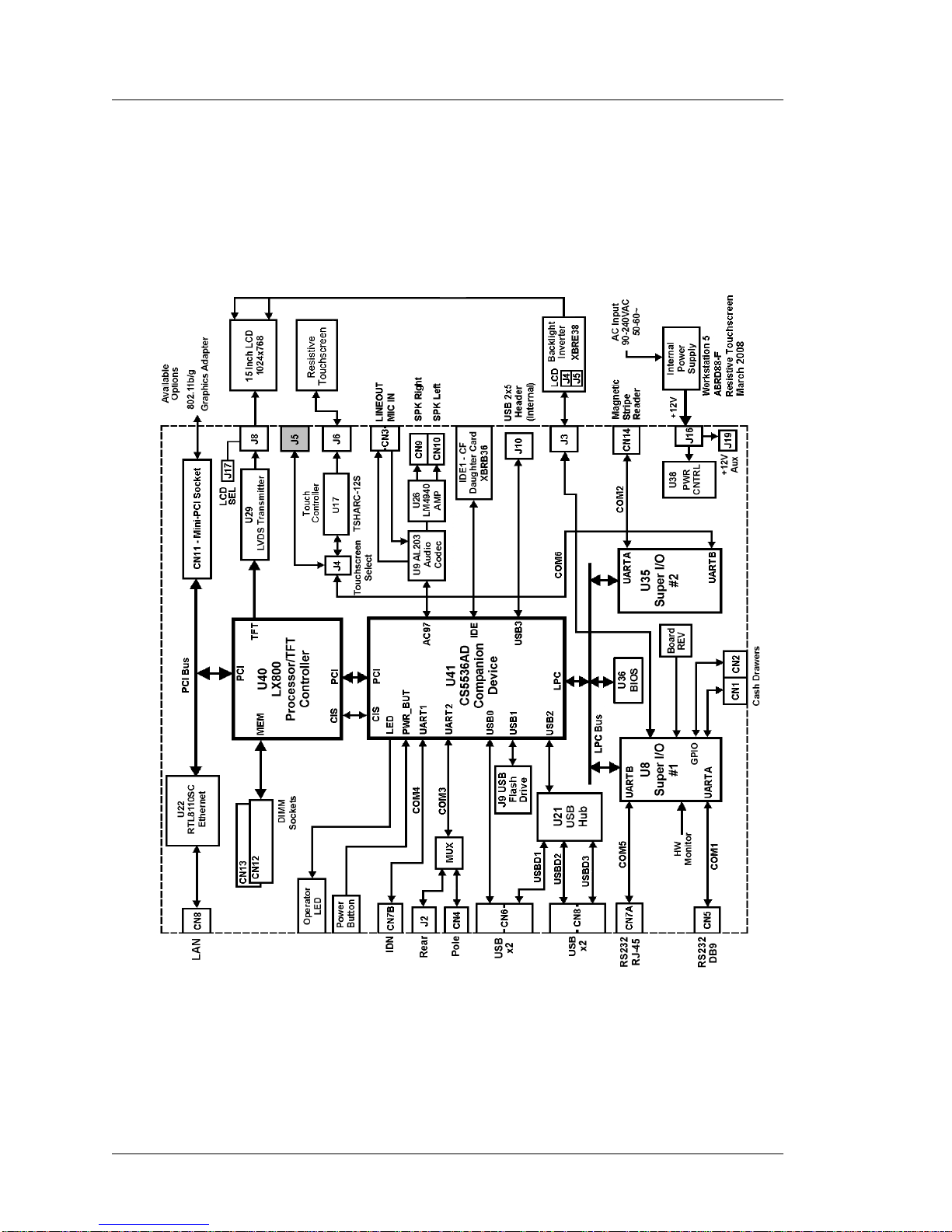
Casework and Mag Card Reader
Casework and Mag Card Reader
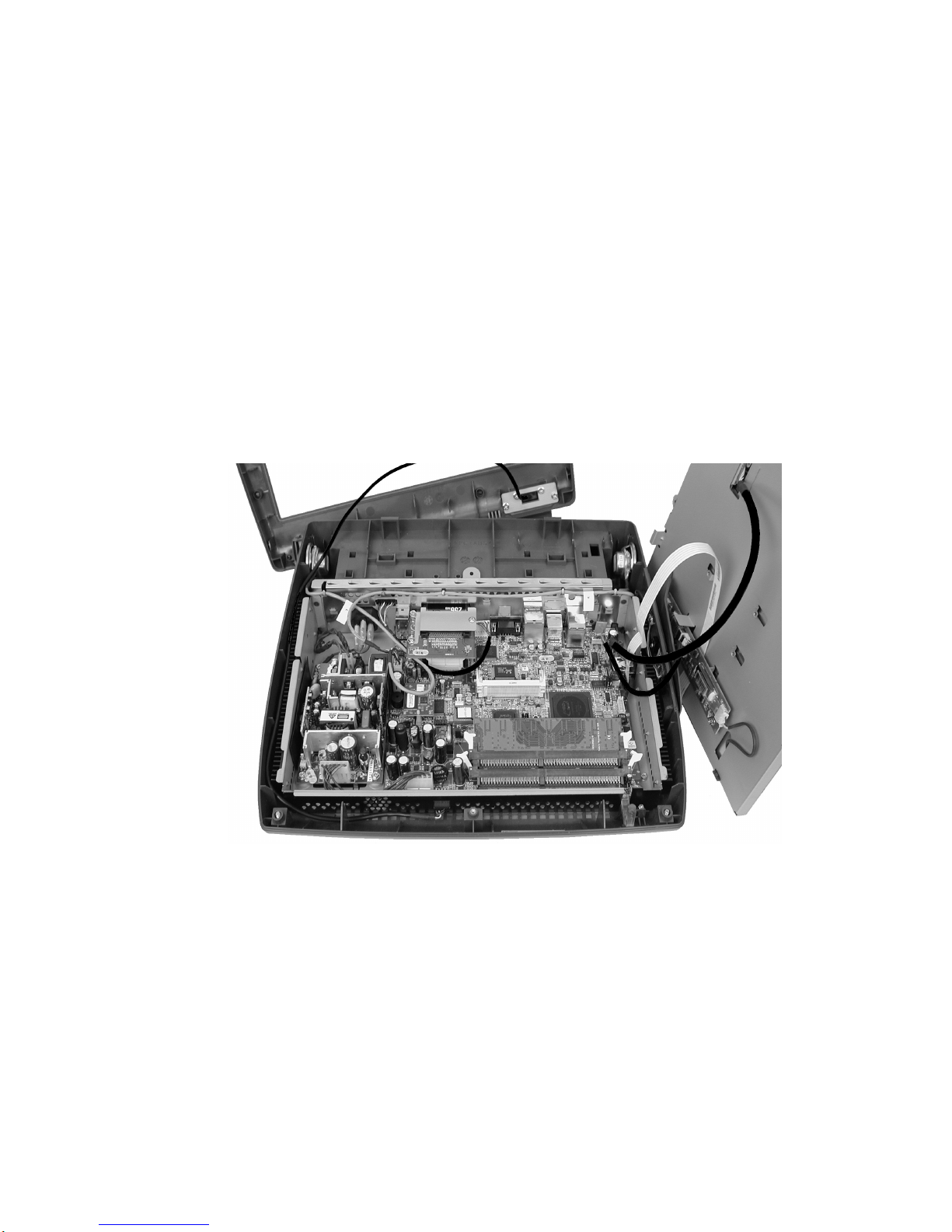
Figure 1-1, below illustrates all plastic components and the Mag Stripe Reader
Assembly.
Figure 1-1: Workstation 5 Casework and Mag Card Reader
• Touchscreen Gasket, Workstation 5 - P/N 600537-128
The touchscreen gasket is pressed into a groove around the inside of the
Top Cover.
• Top Cover, Workstation 5 - P/N 400409-005
Includes Operator LED lens and captive mounting screws pre-installed.
Touchscreen Gasket not included.
Page 16

1-4 Works tat ion 5 Fiel d Servi ce Gui de
Introduction to the WS5 FRUs
Casework and Mag Card Reader
• Door, /w Logo Insert , Work station 5 - P/N 300323-105
Snap-in IO Door with removable MICROS logo insert.
• Base, Workstation 5 - P/N 400408-005
The plastic base holds the chassis, system board, power supply and Mag
Card Reader assembly. Mounting hardware, Mag Card Reader assembly
and power button actuator not included.
• Mag Card Reader Assembly, MCR /w Cable and Cover - P/N 700293-125
Fully assembled Magnetic Card Reader /w cable and plastic mounting
bracket.
• Power Button Actuator, /w Light Pipe and Screw - P/N 300103-011
Power button actuator assembly includes light pipe and mounting screw.
Mounts to the base to activate the System Board power switch.
Page 17
Workst at ion 5 Field S erv ic e Guide 1-5
Introduction to the WS5 FRUs
System B oard and Components
System Board and Compo ne nt s
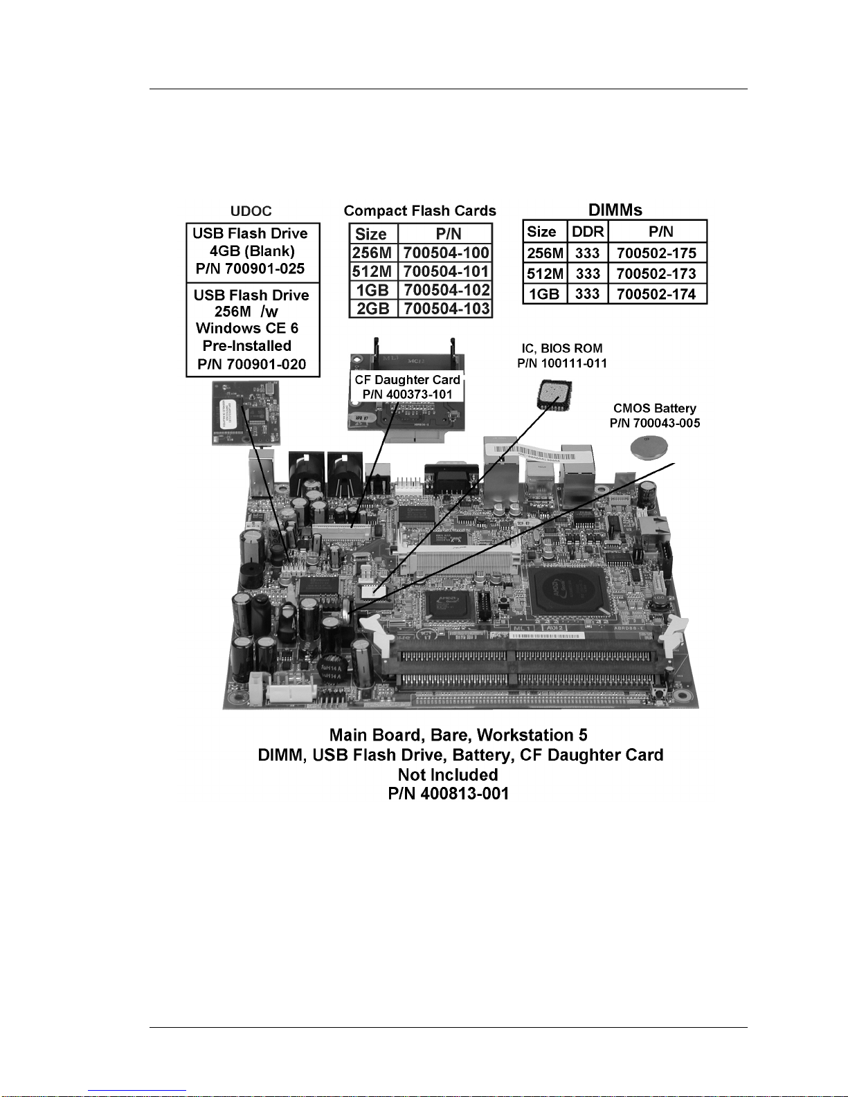
Figure 1-2, below lists the System Board FRU and available components.
Figure 1-2: Workstation 5 System Board and Components
• Main Board, Bar e, Workstation 5 - P/N 400813-001
Bare ABRD88 system board supplied without DIMM, BIOS ROM, USB
Flash Drive, CMOS Battery, or CF Daughter Card.
• USB Flash Drive, 4GB - P/N 700901-025
Blank 4GB USB Flash Drive for WEPOS. Kit P/N 000218-050, the
WEPOS Recovery Kit can be used to restore the WEPOS Flash Drive.
Page 18

1-6 Works tat ion 5 Fiel d Servi ce Gui de
Introduction to the WS5 FRUs
System B oard and Co m ponents
See chapter 3 for more information about recovering the WEPOS image.
• USB Flash Drive, 256M - P/N 700901-020
256M USB Flash Drive is pre-loaded with the Windows Embedded CE 6.0
operating system, platform files and the CAL client utility. Installs on
system board header J9. Not compatible with the Workstation 4 LX System
Board.
• IC, BIOS ROM, WS5 - P/N 100111-011
The pre-programmed 1M BIOS ROM installs in system board socket U36.
Not compatible with the Workstation 4 or Workstation 4 LX.
• Compact Flash Daughter Card - P/N 400373-101
The CF Daughter Card attaches to IDE1 the CF Riser Socket on the
Workstation 5 System Board. Does not include CF Card, cover and
mounting screws. Also compatible with the KWS4, PCWS 2010, the
Workstation 4 and Wor kstation 4 LX.
• Compact Flash Cards - See Figure 1-2
Blank formatted Compact Flash Card in sizes of 256M, 512M, 1GB, and
2GB. The 256M CF is standard for Windows CE, but a WEPOS unit ships
without a CF card installed. Compatible with all CF based MICROS
workstations.
• DIMM, DDR333 256M - P/N 700502-175
DDR3 DIMM suitable for Windows Embedded CE 6.0. Approved devices
include Wintec WD1UN256X808-333B-PH,
WD1UN256X808-333B-PJ-M01, and Unigen
UG732D6688KV-DHFMSS. Also compatible with the Workstation 4 LX.
Please note that the Windows Embedded CE image is limited to 512M of
RAM.
• DIMM, DDR333 512M - P/N 700502-173
Suitable for WEPOS configurations. Wintec part numbers include
WD1UN512X808-333B-QC and WD1UN512X816-333B-PJ-M01.
• DIMM, DDR333, 1GB - P/N 700502-174
Suitable for WEPOS configurations. Wintec Part Number
WD1UN01GX816-333C-QC.
• Battery , CR2032 - P/N 7000043-005
CR2032 Lithium Coin Cell. This battery is also used on the WS4, WS4
LX, PCWS 2010, PCWS Eclipse and KWS4 System Boards.
Page 19
Workst at ion 5 Field S erv ic e Guide 1-7
Introduction to the WS5 FRUs
Power Supply
Power Suppl y
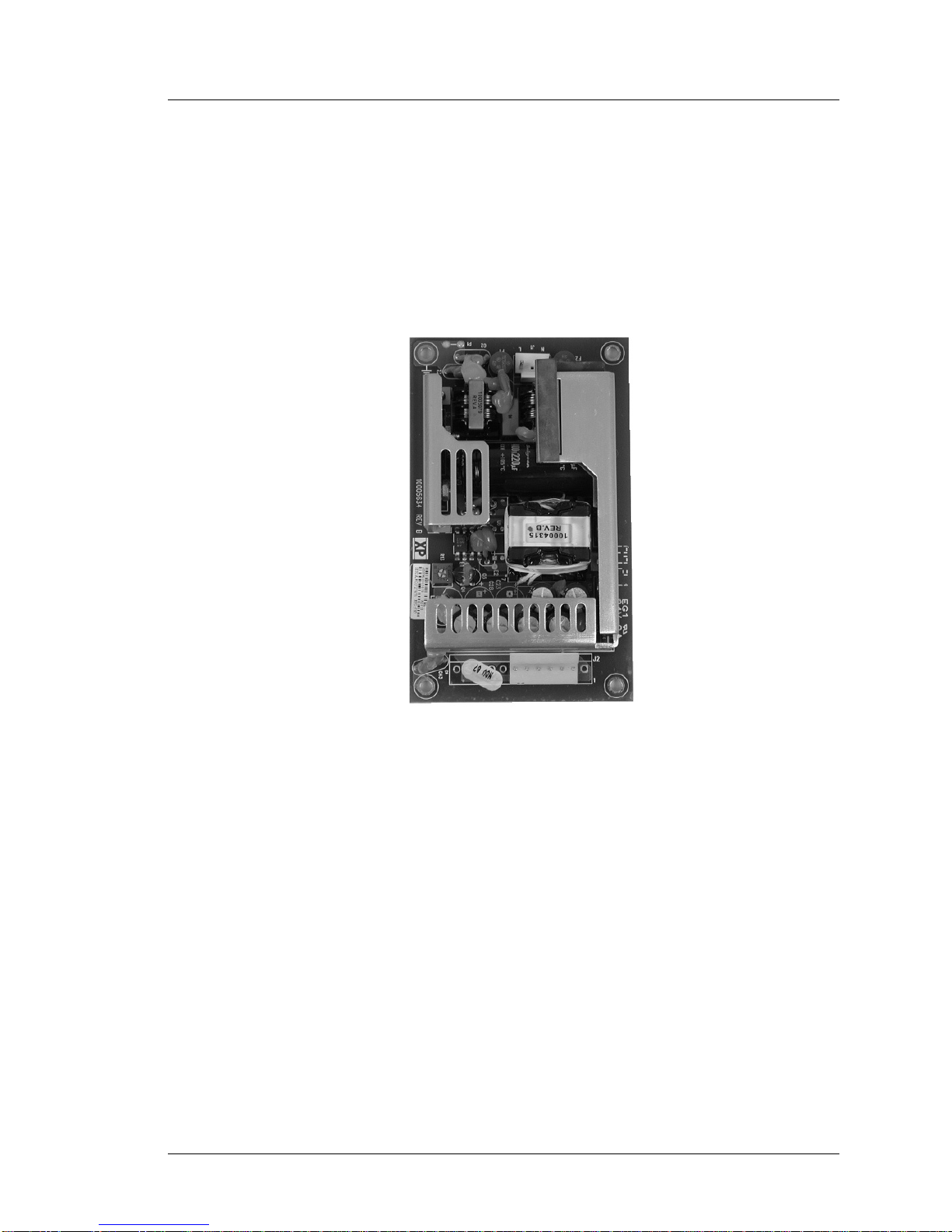
• Power Supply - P/N 700351-022
The +12V 100W open frame power supply is shown in Figure 1-3. Power
Supply vendor and appearance may vary. Not compatible with the
Workstation 4/4 LX.
Figur e 1-3: Workstation 5 Power Supply
Page 20
1-8 Works tat ion 5 Fiel d Servi ce Gui de
Introduction to the WS5 FRUs
LCD and Touchscreen Ass em bly
LCD and Touchscreen Assembly
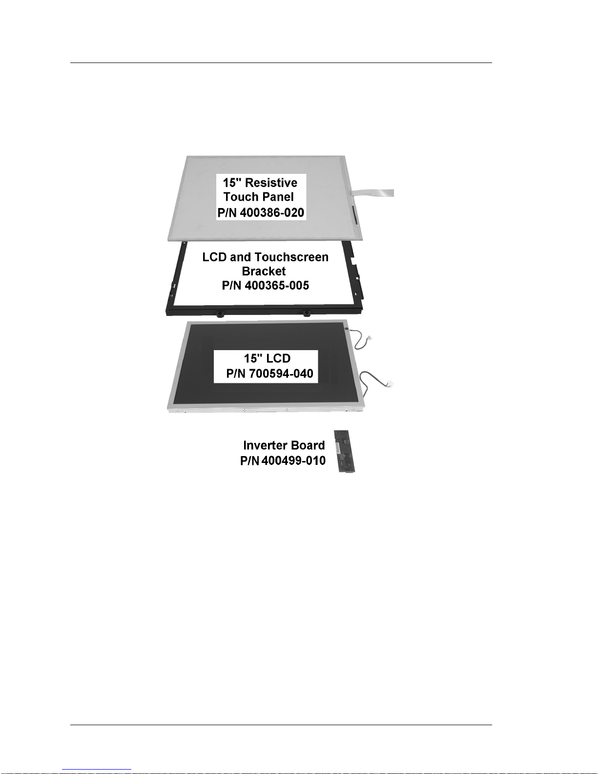
Figure 1-4, displays the FRUs associated with Workstation 5 LCD and
Touchscreen Assembly.
Figure 1-4: LCD and Touchscreen Assembly FRUs
• Touchscreen Panel, 15.0” R esistive, E LO E055550 or EL O E457626 - P/N
400386-020
Five-wire resistive touch panel.
• Bracket, LCD and Touchscreen Assy, /w captive screws - P/N 400365-005
This bracket houses the touchscreen glass and the LCD panel.
• Display 15” LCD, WS5 - P/N 700594-040
Replacement 15” Sharp or AUO LCD Panel. See Chapter 3 for jumper
configurations.
• Inverter Board, WS5 - P/N 400499-010
Workstation 5 compatible push-pull Backlight Inverter Board. Mounts to
the LCD plate. Compatible only with the Workstation 5.
Page 21

Workst at ion 5 Field S erv ic e Guide 1-9
Introduction to the WS5 FRUs
Cables
Cables
This section contains all Workstation 5 internal and external cables.
LCD Data Cable - P/N 300331-305
This cable connects between the System Board J8 and the LCD panel data
connector.
Figure 1-5 : Workstation 5 LCD Data Cable
Cable, Inverter Board - P/N 300331-210
This cable connects between the System Board J3 and J1 on the Backlight
Inverter Board.
Figur e 1-6: Workstation 5 Backlight Inverter Board Cable
Page 22
1-10 Workst at ion 5 F ield S ervi ce Gui de
Introduction to the WS5 FRUs
Cables
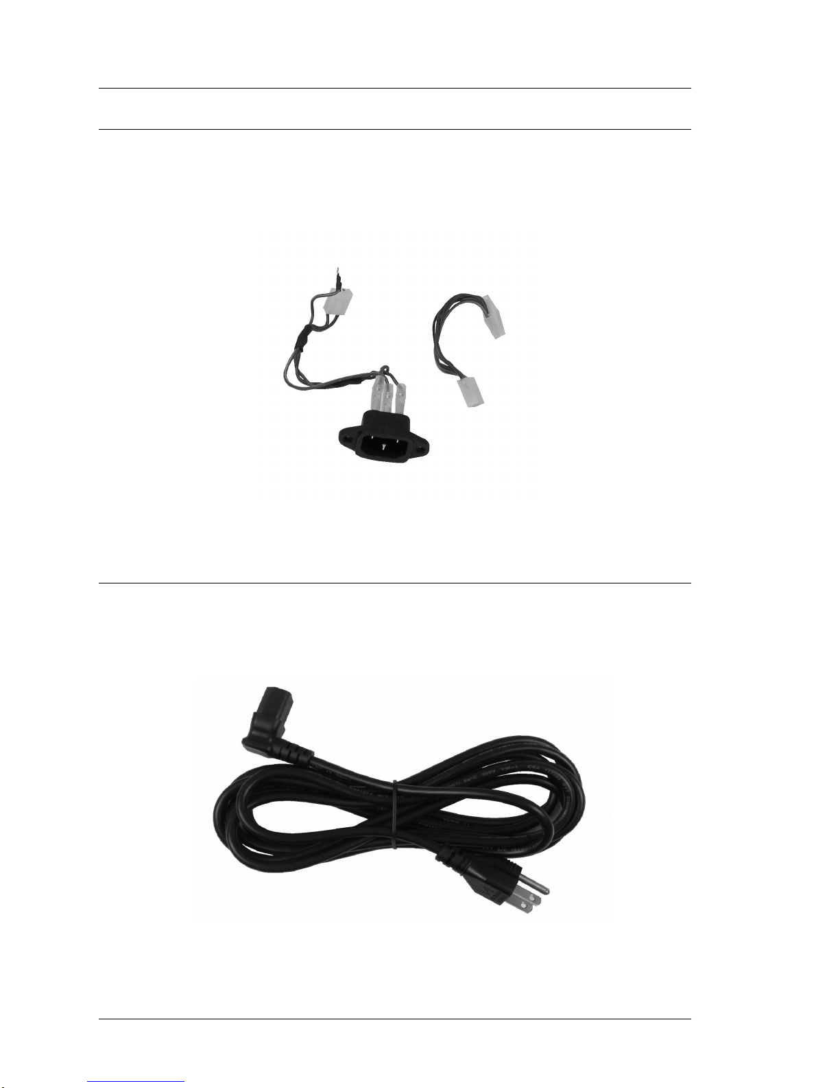
Cable Kit, AC Power In - DC Power Out - P/N 000170-015
Kit consisting of the AC input connector and wiring harness and Power Supply
to the System Board Cable.
Figure 1- 7: Workstation 5 AC In - DC Out Cable Kit
WS5, AC Power Cable, RT Angle - P/N 200153-009
Replacement Power Cable for the Low Profile Workstation 5. Not compatible
with the W orkstation 4/4LX or the Workstation 5 Adjustable Stand.
Figure 1- 8: Workstation 5 Replacement AC Power Cable
Page 23
Workst at ion 5 Field S erv ic e Guide 1-11
Introduction to the WS5 FRUs
Cables
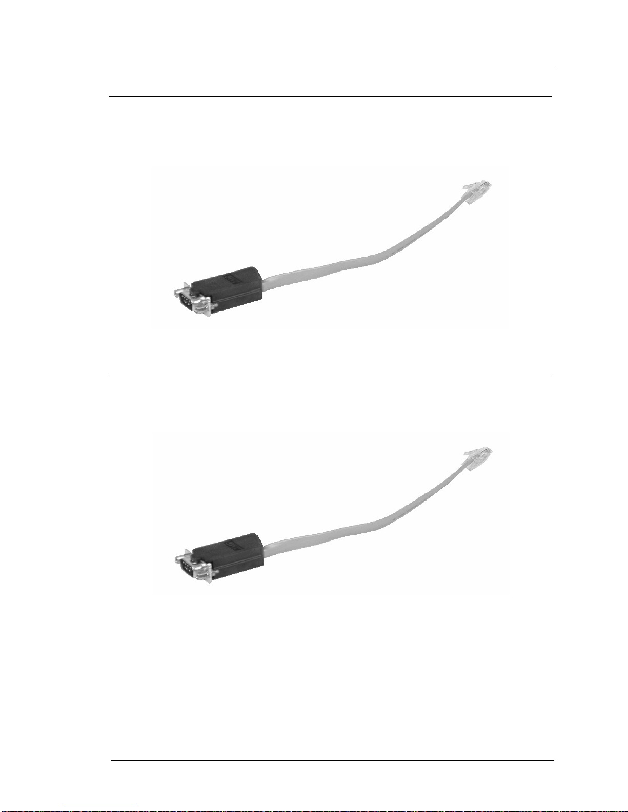
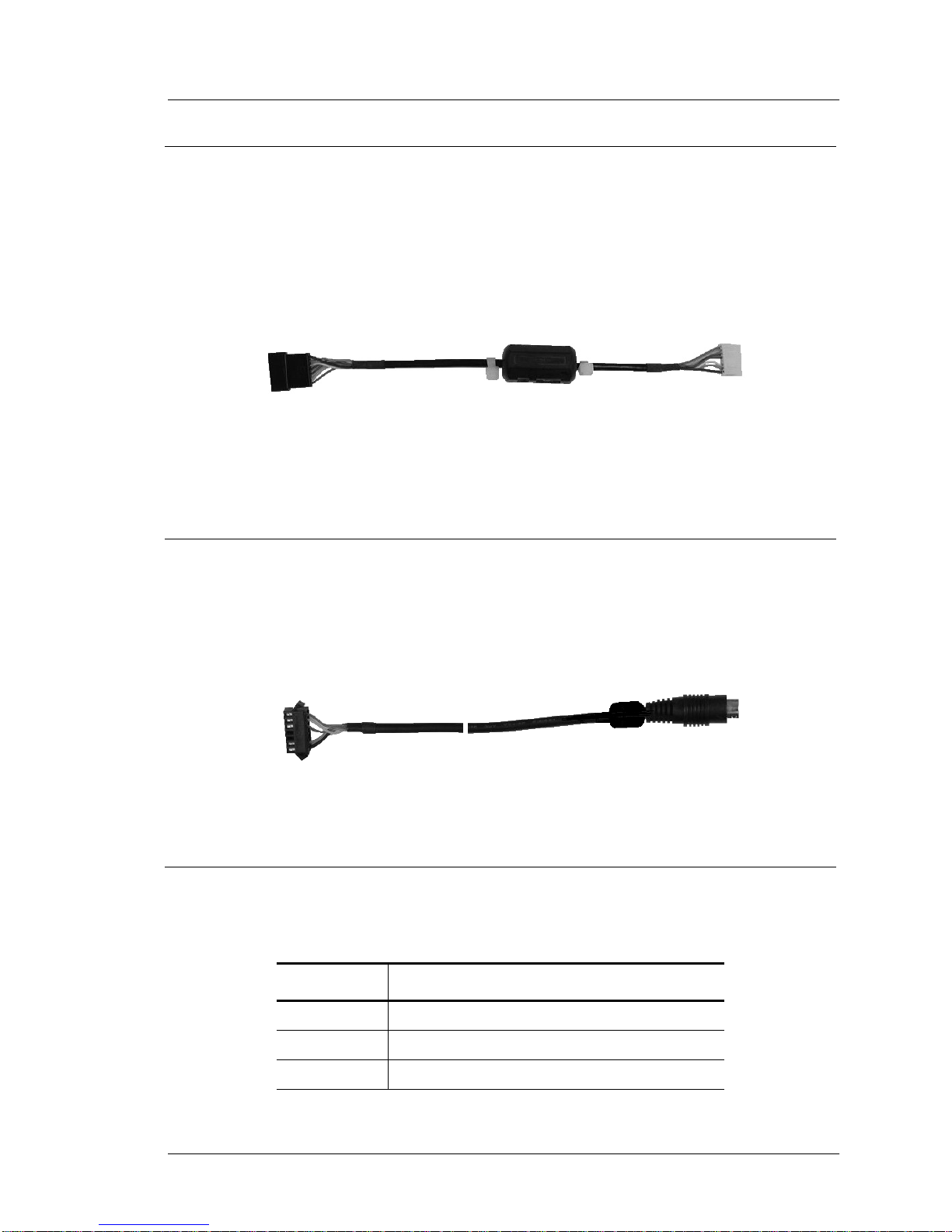
Dongle, RJ45-DB9, IDN Port to RS232 2-Wire Serial - P/N 300319-102
This cable brings out the RS232 conductors from the IDN port to a DB9
connector.
Figure 1-9: Conve rting the IDN Port to RS232 DB9
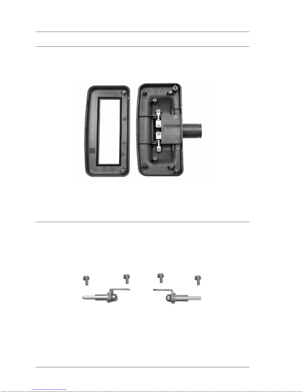
Serial Port Conversion Dongle, COM5, RJ45 to DB9 - P/N 300319-103
This cable converts the modular COM5 serial connector to a DB9 connector.
Figure 1-1 0: Converting the Modular COM5 Port to RS232 DB9
Page 24

1-12 Workst at ion 5 F ield S ervi ce Gui de
Introduction to the WS5 FRUs
Cables
LAN Patch Cables
The table below displays Category 5 Patch Cables in three lengths.
Cash Drawer Extension Cables
For upgrades or under-the-counter installations, the following extended length
cables are available.
Part Number Description
700834-003 Category 5 Patch Cable, Bl ue, 3 Feet
700834-006 Category 5 Patch Cable, Bl ue, 6 Feet
700834-012 Category 5 Patch Cable, Bl ue, 12 Feet
Part Number Description
300029-006 6 Foot Cash Drawer Extender Cable
300029-012 12 Foot Cash Drawer Extende r Cabl e
300029-018 18 Foot Cash Drawer Extende r Cabl e
Page 25

Workst at ion 5 Field S erv ic e Guide 1-13
Introduction to the WS5 FRUs
Workstation 5 Adjustable Stand Acce s s ories
Workstation 5 Adjustable Stand Accessories
USB Extension Cable and Bracket - P/N 400431-305
Optional USB Extension Cable connects between the Workstation 5 IO panel
and the base of the adjustable stand. Cable appearance may vary.
Figure 1-11: Adjustable Stand USB Extension Cable
Third Party Mounting Adapter for Workstation 5 Stand - P/N 600526-050
The mounting adapter installs in place of the WS5 Adjustable Stand Logo
Badge as shown in the Figure below . It can be used to mount a variety
customer facing devices.
Figure 1-12 : Adjustable Stand Third Party Mounting Adapter
Page 26
1-14 Workst at ion 5 F ield S ervi ce Gui de
Introduction to the WS5 FRUs
LCD Customer Display
LCD Customer Display
This section lists the available FRU’s for the LCD Customer Display. See
Chapter 6 for instructions on removing and replacing these items. The WS4,
KWS4, WS4 LX and WS5 support this display.
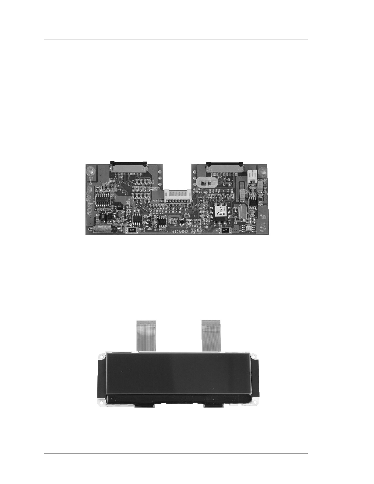
LCD Interface Board - P/N 400702-001
The LCD Customer Display Interface Board is used for the Integrated, Pole
and Adjustable Stand Pole mounted display. This board also drives the
Operator Display in the KWS4.
Figur e 1-13: LCD Customer Display Interface Board
LCD Module, Optrex - P/N 700594-117
The 240x64 Monochrome LCD Module is used for the Rear and Pole Mount
LCD Customer Display . It is also used for the Operator Display on the KWS4.
Figur e 1-14: Optrex LCD Module for the LCD Customer Display
Page 27
Workst at ion 5 Field S erv ic e Guide 1-15
Introduction to the WS5 FRUs
LCD Customer Display
Cable, LCD Pole and Rear Display Head - P/N 300331-251
This replacement cable connects between the LCD Interface Board in the rear
or pole LCD display housing to cable 400446-007 (Integrated/Rear) or
300331-250 (Pole).
Figure 1-15 : Replacement LCD Customer Display Cable
Cable Extension, LCD Pole Display - P/N 300331-250
This cable is installed in the pole and connects between 300331-251 (above)
and the WS4, WS4 LX, WS5 or KWS4 I/O Panel.
Figure 1-16: Replacement LCD Pole Extension Cable
LCD Customer Display Poles
Three sizes are available, they can be used as a replacement or conversion for
kit 500827-007, or 700827-105.
Part Number Description
600568-031 Replacement 6 Inch Pole
600568-032 Replacement 12 Inch Pole
600568-033 Replacement 18 Inch Pole
Page 28
1-16 Workst at ion 5 F ield S ervi ce Gui de
Introduction to the WS5 FRUs
LCD Customer Display
Kit, Front/Rear Cover, /w Lens, Screws, Pole Mount Hinge - P/N 000160-010
LCD Customer Display housing kit with Front and Rear Plastic covers, pole
mount and pre-installed 2nd generation hinge assembly.
Figure 1-17: Pole Display Plastic Replacement Kit
Workstation 5 Integrated LCD Bracket is not yet available. The WS4 WS4LX
bracket is not compatible.
Hinge Set, LCD Customer Display - P/N 400456-020
The hinge set can be used on the updated LCD Customer Display housing rear
cover.
Figure 1-18: Rea r/Pole Hinge Set /w Mounting Screws
Page 29

Workstation 5 Field Ser vic e Guide 2-1
Chapter 2
Workstation 5 System Board
Technical Descriptions
This chapter provides technical descriptions of the Workstation 5
System Board and accessories.
In this chapter
Workst a t i o n 5 Sys t e m Bo a rd Block Diagram.................................... 2-2
LX800 Processor and TFT Controller ...............................................2-4
CS5536 Companion Device...............................................................2-8
TFT LCD an d Ba cklight Int e rface...... .............................................2-12
USB Interface ..................................................................................2-16
T ouchscreen Interface......................................................................2-19
LPC Inte rface.... ...............................................................................2-20
AC 97 Audio In t e rface.. ...................................................................2 -21
Point Of Sale Interfaces.... .... ........... .... ...... .... ...... .... ...... .... ...... .... ....2- 23
RTL8110SC Ethernet Controller .....................................................2-32
System Board Power Distribution ...................................................2-34
Page 30
2-2 Workstat io n 5 Fie ld S ervice Guide
Workstation 5 System Board Technical De scriptions
Workstation 5 System Board Block Diagram
Workstation 5 System Board Block Diagram
Figure 2-1 displays a block diagram of the Workstation 5 with the standard
resistive touchscreen. This configuration represents production units from
January 2008 to February 2009.
Figure 2-1: Workstation 5 Block Diagram /w Resistive Touchscreen
Page 31

Workstation 5 Field Ser vic e Guide 2-3
Workstation 5 System Board Technical Descriptions
Workstation 5 System Board Block Diagram
Figure 2-2 below displays a block diagram of the Workstati on 5 with an
optional capacitive touchscreen installed. This configuration adds the
Capacitive Touchscreen Interface Board. This configuration is not in
production,
Figure 2-2 : Workstation 5 Block Diagram /w Capacitive Touchscreen
Page 32

2-4 Workstat io n 5 Fie ld S ervice Guide
Workstation 5 System Board Technical De scriptions
LX800 Processor and T FT Co nt roller
LX800 Processor and TFT Controlle r
REF: ABRD88 - Sheets 1, 2, 5 and 6
Figure 2-3 displays a block diagram of the LX800 processor.
Figure 2-3: AMD Geode LX800 Processor/TFT Controller Block Diagram
Page 33

Workstation 5 Field Ser vic e Guide 2-5
Workstation 5 System Board Technical Descriptions
LX800 Process o r a n d TFT C on trolle r
Processor Core
The processor core consists of an integer unit, cache memory subsystem, and
an x87 compatible floating point unit. The integer unit contains the instruction
pipelines and associated logic. The memory subsystem contains the instruction
and data caches, translation look-aside buffers (TLBs) and an interface to the
GeodeLink Interface Units (GLIUs).
The LX800 instruction set is based on a combination of Intel’s Pentium®, the
AMD K6® processor, and the Athlon™ Floating point unit, and the AMD
Geode™ LX processor specific instructions.
GeodeLink Interface Units
The pair of GeodeLink Interface Units (GLIU0 and GLIU1 in the LX800 block
diagram, Figure 2-3) form the heart of GeodeLink architecture. Each features a
built-in arbiter that enables dynamic allocation of memory bandwidth, with
on-the-fly prioritization.
Internally each GLIU includes seven channels, with channel 0 reserved for the
GLIU itself and not considered a physical port. Together, GLIU0 and GLIU1
make up the internal bus comprised of the GeodeLink architecture. GLIU0
connects to the five modules that require high bandwidth, and GLIU1 connects
to the five low bandwidth modules.
GLIU0 is connected to modules with high-bandwidth requirements:
•CPU Core
• GeodeLink Memory Controller (GLMC)
• Graphics Processor
• Display Controller
• GLIU1 (GeodeLink Interface Unit 1).
GLIU1 is connected to modules with lower bandwidth requirements:
• GeodeLink Control Processor (GLCP)
• Video Input Port
• GeodeLink PCI Bridge
• TFT Controller/Video Output Port (VOP)
• Security Block.
Page 34

2-6 Workstat io n 5 Fie ld S ervice Guide
Workstation 5 System Board Technical De scriptions
LX800 Processor and T FT Co nt roller
GeodeLink Memory Controller
The GeodeLink Memory Controller provides all of the LX800 memory needs.
The GLMC is capable of ha ndling multiple requests for memory data fr om the
CPU core, the Graphics Processor, the Display Controller and the external PCI
bus via the GeodeLink Interface Units (GLIUs). Contention for memory
bandwidth between the various modules is minimized by extensive buffering
logic.
Because the GLMC supports the memory requirements of both the CPU core
and display sub-system, it is classified as a Unified Memory Architecture
(UMA) subsystem.
• The 64-bit DDR SDRAM Interface as implemented on the LX System
Board, supports unbuffered DDR 333/400 DIMMs up to 2GB.
• Unified Memory Architecture (UMA), UMA enables up to 2GBps memory
bandwidth while using single memory interface. The DDR Memor y array
contains both the main system memory and the graphics frame buffer.
GeodeLink Control Processor
The GeodeLink Control Processor is used for software debugging and
performance analysis.
GeodeLink PCI Bridge
The GeodeLink PCI Bridge (GLPCI) module provides the PCI interface for the
LX800 system. It is comprised of five major sections or blocks, briefly
described below.
GeodeLink Interface Block
The GeodeLink Interface Block provides a conversion layer between the
GeodeLink Interface Unit 1 (GLIU1) and the Transaction Forwarding
Block.
FIFO/Synchronous Block
The FIFO module consists of a group of in-bound and out-bound FIFOs.
Each FIFO provides a simple, synchronous interfaces to read and write
requests.
Transaction Forwarding
The Transaction Forwarding block receives, processes and forwards
transaction requests and responses between the GeodeLink Interface and
PCI Bus Blocks. Transaction ordering rules are implemented and write
gathering and read pre-fetching are performed as required.
Page 35

Workstation 5 Field Ser vic e Guide 2-7
Workstation 5 System Board Technical Descriptions
LX800 Process o r a n d TFT C on trolle r
PCI Bus Interface Block
The PCI Bus Interface provides a protocol conversion layer between the
transaction forwarding block and the PCI bus. The master and target
portions of this block operate independently.
The PCI Bus Interface Block impl ement s the logic to generate PCI
configuration cycles. The standard mechanism for generating PCI
Configuration cycles (as described in the PCI 2.2 Specification) is used.
PCI Bus Arbiter
The PCI Arbiter implements a fair arbitration scheme with special support
for the CD5536 companion device. By default it operates as a simple round
robin arbiter that rotates three request/grant prioritie s in a circular fas hion.
GeodeLink Interface General Description
The GeodeLink Interface is a non-traditional high bandwidth packetized
uni-directional bus for internal peripherals. The GeodeLink architecture
connects the internal modules of the LX800 and companion device using
the data ports defined by GeodeLink Interface Units. Transactions between
GeodeLink Devices and the GLIU are conducted with packets.
The GLIU accepts request packets from masters and routes them to slaves.
Similarly, slave response packets are routed back to the master. The bus is
non-blocking. Several requests can be pending, but order is not guaranteed.
All packets have one source and one destination, broadcasts are not
allowed.
The existence of the GeodeLink architecture is generally invisible to the
user or even a system programmer. All GeodeLink initialization and
support is handled at the BIOS level, and additionally provides a Virtual
PCI Configuration Space to abstract the GeodeLink architectur e to
industry standard interfaces. Through the V irtual PCI Configuration Space,
all GeodeLink devices appear in one PCI multi-function configuration
space header on the external PCI bus.
Page 36

2-8 Workstat io n 5 Fie ld S ervice Guide
Workstation 5 System Board Technical De scriptions
CS5536 Co m p anion Device
CS5536 Companion Device
REF: ABRD88 - Sheets 8, 9 and 10
The CS5536 Companion Device is designed to work with the LX800, a
processor with an integrated memory controller. Together, the LX800
processor and CS5536 Companion Device provide a low power, high
performance embedded solution for both the Workstation 4 LX and the
Workstation 5.
The internal architecture is based on the high-performance GeodeLink
architecture that yields high internal speed (over 4 GB/s) data movement and
versatile power management.
Communications with the AMD LX800 processor is over the 66Mhz PC I Bus.
The Geode Companion device includes many IO functions on-chip. These
include:
System Management Bus (SMB) Controller
The SMB is a two-wire synchronous serial interface compatible with the
System Management Bus physical layer. On the WS5 system board, the
SMB controller in the Companion Device is connected to Ethernet
Controller U22, as well as each DDR DIMM socket.
Serial Interface
The CS5536 includes two high-speed industry standard serial ports,
configured to support the Customer Display and IDN Interfaces. The
UAR Ts are 16550 and 16450 software compliant and support baud rates up
to 115.2 kbps.
Real Time Clock (RTC) and CMOS RAM
The companion device contains the equivalent of Motorola MC146818A
compatible real time clock. The clock performs two functions. It keeps
track of the time and date when the system is not connected to AC power,
and provides 242 bytes of non-volatile memory for storing BIOS and
system data.
The clock contains separate registers for seconds, minutes, hours, days
(both day of week and day of month), months, and years. The RTC
operates from a 32.768 Khz crystal and is powered from a 3V lithium
battery that can maintain operation for several years.
ATA Interface
The IDE Interface is an ATA-5 specification compatible IDE controller
(ATAC). Two devices are supported, using PIO Modes 0 through 4,
MDMA modes 0 to 2, and UDMA/66 mode 0 through 4.
Page 37

Workstation 5 Field Ser vic e Guide 2-9
Workstation 5 System Board Technical Descriptions
CS5536 Com p an io n D evic e
The interface provides a variety of features to optimize system
performance, including 32-bit disk access, post write buffers, bus master,
look-ahead read buffer, and pre-fetch mechanism.
On the WS5 System Board, the CF Card resides on the ATA Interface in
socket IDE1.
USB Interface
The CS5536 Companion Device includes four Universal Serial Bus (USB)
2.0 compliant ports, supporting low speed, full speed, and high-speed
connections.
Each port supports wake-up events and feature over-current and power
control support. The ports can be enabled individually to react to
over-current events.
Port 4 supports the USB 2.0 On-The-Go supplement version 1.0
specification, but this feature is not supported on the WS5 system board.
One USB output from the Companion Device is fed to an on-board USB
hub controller. See the System Board USB Interface Section for more
information.
LPC Interface
The LPC is based on Intel’s Low Pin Count (LPC) specification version
1.0. The controller can convert an internal local bus memory or IO cycle to
an external LPC cycle. It receives serial IRQs from the LPC bus and
converts them to parallel form so they can be routed to the IRQ mapper and
interacts with the Legacy DMA logic to perform DMA between on-chip
and off-chip devices.
The LPC interface supports memory, I/O, DMA, and firmware hub based
devices.
Audio Codec Interface
The codec interface is AC97 V2.3 compliant and contains support for any
AC97 audio codec with Sample Rate Conversion (SRC). The WS5 S ystem
board uses a Realtek ALC203 Audio Codec and audio amplifier to drive a
pair of internal speakers. See the AC 97 Audio Interface section for more
information.
Diverse Device
The Diverse Device is comprised of the legacy PC functionality required
for most designs.
Page 38

2-10 Workstat io n 5 Fie ld S ervice Guide
Workstation 5 System Board Technical De scriptions
CS5536 Co m p anion Device
Power Management Controller (PMC)
This module is a GeodeLink Device whose functio n is to control all aspects
of power management. Power Management is event driven - any action the
PMC carries out is predicated on some event. Those events can originate
from other GeodeLink Devices, such as the LX800 processor, or from
other external sources such as the power button.
The PMC consists of three internal sections: Working, Standby, and Real
Time Clock.
o The Working block includes all circuits and functions associated with
the W orking power domain. The primary function of the Wor king block
is to transition the system to the sleep mode.
o Standby block contains all circuits and functions associated with the
Standby power domain. The primary function f the Standby block is to
control power to the Working domain.
o The RTC block contains the timing circuits required to maintain a real
time clock and calender functions. The R T C block is powered by
VBAT, from a board mounted CR2032 battery.
Page 39

Workstation 5 Field Ser vic e Guide 2-11
Workstation 5 System Board Technical Descriptions
CS5536 Com p an io n D evic e
IDE Interface (REF: ABRD88 - Sheet 18)
Figure 2-4 displays a block diagram of the WS5 System Board IDE Interface
coupled to the CF Daughter Card.
Figur e 2-4: Workstation 5 IDE Interface Block Diagram
Like the Workstation 4, the CF Daughter card is positioned to make the CF
card available at the IO panel where it can serve as a ‘personality’ module in
Windows Embedded CE 6.0 configurations.
LED1 is the hard disk activity indicator and is located just to the left of the
mini-DIN pole customer display connector.
The CF card is an intelligent solid state storage device containing a micro
controller and firmware positioned in front of a block of flash memory. The
firmware responds to file IO requests from the operating system file driver and
maps file data to/from the flash memory array.
Page 40

2-12 Workstat io n 5 Fie ld S ervice Guide
Workstation 5 System Board Technical De scriptions
TFT LCD a n d B acklig ht In terface
TFT LCD and Backlight Interface
REF: ABRD88 - Sheets 27
Figure 2-5 displays a block diagram of the LX800 Processor with the TFT
controller sections highlighted. The LX800 graphics interface consists of the
Graphics Processor (GP), the Display Controller (DC) and the V ideo P rocessor
(VP).
Figur e 2-5: LX800 Graphics Processor Block Diagram
The Graphics Processor (GP)
The Graphics Processor is based on the Graphics processor used in the Geode
Processor, but adds the GeodeLink memory interface and other features to
support improved performance and functionality.
The GP is a BitBL T/vector graphics engine, that supports pattern generation,
source expansion, pattern/source transparency, 256 ternary raster operations,
alpha blenders to support alpha-BLTs, incorporated BLT FIFOs, and
GeodeLink interface.
Page 41

Workstation 5 Field Ser vic e Guide 2-13
Workstation 5 System Board Technical Descriptions
TFT LCD and Back light Interface
The Display Controller (DC)
The DC module is similar to that found in the Geode GX processor line with
additional hardware for graphics filter functions. It consists of a memory
retrieval system (GLIU0), Graphical User Interface (GUI) block, a VGA
interface block, and back-end filter/scaling. The GUI and VGA blocks share a
single display FIFO and display refresh memory interface to the GeodeLink
Memory Controller (GLMC).
The DC module retrieves graphics, video, and overlay streams from the frame
buffer, serializes the streams, performs any necessary color look-ups and
output formatting, and interfaces to the Video Processor for driving the display
device.
Video Processor (VP)
The VP interfaces with the processor core via a GLIU master/slave interface to
provide three main functions, the V ideo Processor, the TFT controller, and the
V ideo Output Port (VOP). The VP mixes the graphics and video streams, and
outputs digital RGB data to the TFT Controller.
The TFT Controller converts the digital RGB output of the V ideo Mixer block
to the digital output suitable for driving a TFT flat panel LCD. The panel
interface supports most SVGA TFT panels and meets the VESA FPDI (Flat
Panel Display Interface) Revision 1 Specification including the correct power
sequencing.
Page 42

2-14 Workstat io n 5 Fie ld S ervice Guide
Workstation 5 System Board Technical De scriptions
TFT LCD a n d B acklig ht In terface
LCD Interface (REF: ABRD88 - Sheets 5, 16 and 27)
Figure 2-6 displays a block diagram of the Workstation 5 LCD and Backlight
Interfaces.
LX800 Pixel Data outputs DRGB[23:2] are fed to U29, a THC63LVDM83R
LVDS Trans mitter. This device contains four seven-bit parallel-load serial-out
shift registers coupled to low voltage differential signalling (LVDS) line
drivers. Its primary function is to convert the 28-bits of Low Voltage TTL level
pixel, control and clock data from the LX800 TFT Controller into four data
streams and a single clock stream. The output of U29 drives LCD connector
J8.
The primary reasons for converting the TTL/CMOS level video signals to the
LVDS format are reduced noise and cable pin count. The LVDS compatible
signals are converted back into Low V olt age TTL/CMOS voltage levels within
the LCD Panel.
LCD Panel power sequencing is provided by the VDDEN_VIPSYNC output of
the LX800 TFT controller. This signal drives a switch consisting of Q9 and
Q10. VDDEN_VIPSYNC does not go active until all system voltages and
busses have become stable and the processor is executing instructions.
Figure 2-6: WS5 Syst em Board TFT LCD and Backlight Interface
Page 43

Workstation 5 Field Ser vic e Guide 2-15
Workstation 5 System Board Technical Descriptions
TFT LCD and Back light Interface
Backlight Interface
The backlight enable signal, DISPEN originates in the LX800 TFT controller.
This enable signal is ANDed with
SIO_PWM at U6 to produce PWMBL which
drives the backlight inverter board mounted to the LCD plate. SIO_PWM
originates from an unused fan controller (FANPWM2) in Super I/O #1, U8.
Inverter Board power, VCC_BL is supplied by VCC12 through F1 and FB8. A
pre-regulator circuit is not implemented on the WS5 System Board.
Configuration Jumpers
A total of three jumpers, one on the system board and two on the inverter
board are required to configure the LCD panel type.
System Board jumper J17 is used for LCD Panel configuration. At this
time, one of two possible LCD panels may be used. Production started with
the Sharp LQ150X1LG45 15” LCD Panel and J17 includes a jumper
placed between Pins 1 and 2. Note that Pin-1 faces the rear of the unit. On
later units with an AUO LCD Panel is installed, no jumper will be installed
on J17.
The Backlight Inverter Board contains a pair of jumpers J4 and J5, factory
configured to match the LCD panel installed. The jumper setting is routed
through the interface cable to the system board as BL_MOD0 and
BL_MOD1 and fed to a pair of general purpose (GPIO28 and GPIO29)
inputs on Super IO #1, U8.
At power-up, the WS5 API reads this pair of bits to determine the LCD
panel type. When it determines the LCD panel type, for example the Sharp,
it references the \DOC\HWInf folder and loads the file
‘lxvideo_Sharp.inf.’ This file contains backlight brightness and brightness
range values optimized for the Sharp LCD. If the AUO panel is used, the
jumpers are set accordingly and the API would load the ‘lxvideo_auo.inf
file from the \DOC\HWInf folder.
Page 44

2-16 Workstat io n 5 Fie ld S ervice Guide
Workstation 5 System Board Technical De scriptions
USB Interface
USB Interface
REF: ABRD88 - Sheets 9, 16, 21, and 29
The Workstation 5 System Board includes a total of seven USB ports, four of
which are available at the IO Panel. A fifth USB port is accessible at the front
of the chassis for the integrated finger print reader or other optional device.
Figure 2-7 displays a block diagram of the system board USB interface
including the USB port assignments and the power management scheme.
Figure 2-7: Workstation 5 System Board USB Configu ration
Page 45

Workstation 5 Field Ser vic e Guide 2-17
Workstation 5 System Board Technical Descriptions
USB Interf ace
Companion Device
U41, the CS5536 companion device supplies four USB ports. One port, USB0
is fed to IO panel connector CN6A.
The USB1 output drives J9, the USB Flas h Drive Connector.
USB Flash Drive Power Control
In the Windows Embedded CE 6.0 and current WEPOS configuration, the
USB Flash Drive is the primary boot device. A pre-boot POST test ensures
the device is installed.
However, to provide the flexibility of booting from the CF Card, a BIOS
field is available that removes power from J9, the USB Flash Drive
connector.
A GPIO signal from U8, Super IO #1 called UDOC_ON is controlled by
the ‘Boot Test Image’ field of the Special Configuration screen of BIOS
Setup. UDOC_ON drives a switch consisting of Q6 and Q8. The default
setting of ‘Normal’ sets UDOC_ON high, enabling the switch and
providing VCC5_UDOC to power the USB Flash Drive.
When the Boot Test image field is set to ‘Alternate,’ UDOC_ON goes low,
and turns off switch, cutting power to the USB Flash Drive socket.
Using the ‘Reset BIOS to WI NCE or WINXPE defaults’ automatically s ets
the Boot Test Image field to ‘Normal,’ to allow booting from the USB
Flash Drive.
The USB2 port drives the input of USB Hub U21, a device that adds three US B
ports to the System Board. See below.
The USB3 port drives J10. This is a right angle 2x5 connector positioned at the
front edge of the system board and accessed through a cut-out in the cage.
Currently the optional Integrated Finger Pr int Reade r is connecte d to this port.
Future options could also use this USB Port.
CN6 Port Power
U30, an LM3526 Dual Port USB Power Switch handles the power and
current-limiting requirements of dual USB connector CN6. The device
contains a pair of P-channel MOSFETS (one for each port) with separate
enables and fault outputs. In a typical application, current flows from the
IN(put) pins through the MOSFET and OUT towards the load.
The device employes a two-stage thermal protection circuit. If the internal
temperature is greater than 150°C, both MOSFETs are turned off and the
fault outputs, FLAGA# and FLAGB# go active. These outputs have a 1 ms
delay to prevent false over-current reporting from the in-rush current
caused by hot plug events. Shorted switches will continue to cycle off and
on, due to the rising and falling die temper ature, until the s hort is removed.
Page 46

2-18 Workstat io n 5 Fie ld S ervice Guide
Workstation 5 System Board Technical De scriptions
USB Interface
USB Hub
The USB2 port from the Companion Device is fed to USBDP0, the upstream
port of U21, an SMSC 2503 3-port hub. The device is fully compatible with
the USB 2.0 specification. It adds three additional USB Ports, assigned to the
following connectors.
The USBDP1 port is fed to IO port connector CN6B.
The USBDP2 and USBDP3 ports are fed to IO Port Connector CN8.
CN8 Port Power
U16, an LM3526 Dual Port USB Power Switch handles the power and
current-limit requirements for dual USB connector CN8. The device
contains a pair of P-channel MOSFETS (one for each port) with separate
enables and fault outputs. In a typical application, current flows from the
IN(put) pins through the MOSFET and OUT towards the load.
The device employes a two-stage thermal protection circuit. If the internal
temperature is greater than 150°C, both MOSFETs are turned off and the
fault outputs, FLAGA# and FLAGB# go active. These outputs have a 1 ms
delay to prevent false over-current reporting from the in-rush current
caused by hot plug events. Shorted switches will continue to cycle off and
on, due to the rising a nd falling die temperature, until the short is removed.
Page 47

Workstation 5 Field Ser vic e Guide 2-19
Workstation 5 System Board Technical Descriptions
Touchscreen Int er face
Touchscreen Interface
Figure 2-8 shows a block diagram of the system board resistive touchscreen
interface.
Figur e 2-8: WS5 5-Wire Resistive Touchscreen Interface
U17, the Hampshire TSHARC-12S resistive touchscreen controller is a single
chip design, incorporating a microprocessor, A/D converter, UART, and
firmware. It supports only 5-wire resistive touchscreen and serial interface to
the host system.
The serial Receive/Transmit signals from U17 are routed to jumper block J4.
When a resistive touchscreen is inst all ed, J4 is configured to route RES_TXD
to F_TXD2 and RES_RXD to F_RXD2 which are fed to UART2 in U35 Super
IO #2.
When the optional Capacitive Touchscreen Interface Board is installed, the
jumpers are configured to route CAP_TXD and CAP_RXD to U35 instead of
the resistive touchscreen controller.
Page 48

2-20 Workstat io n 5 Fie ld S ervice Guide
Workstation 5 System Board Technical De scriptions
LPC Interface
LPC Interface
The Low Pin Count Interface is a PCI like-bus comprised of seven signals lines
and is used to replace the legacy ISA bus as the interface between the
Companion Device and Super IO and BIOS devices. Figure 2-9 below displays
a block diagram of the LPC Bus as implemented on the Workstation 5 System
Board.
Figure 2-9: LPC Bus Block Diagram
A total of three devices and the LPC Debug slot are attached to the LPC Bus.
Because the LPC Bus is a replacement for th e legacy for the ISA Bus, the
BIOS redirects Port 80H POST Codes to the LPC Bus.
Two lines from the Companion Device, BOS0 and BOS1 specify location of
the Boot Device after a hardware reset. These pins are configured to ‘Boot
from a Memory Device on the LPC Bus,’ in this case BIOS EEPROM U36.
Page 49

Workstation 5 Field Ser vic e Guide 2-21
Workstation 5 System Board Technical Descriptions
AC 97 Audio Interface
AC 97 Audio Interface
Figure 2-10 displays a block diagram of the WS5 System Board AC’97 Audio
Interface.
Figure 2-10: Workstation 5 Audio Circuit Block Diagram
Realtek ALC203E Features
• Compliant with AC97, 2.3 Specification
• Meets performance requirements for audio on PC99/2001 systems.
• Meets Microsoft WQHL/WLP 2.0 audio requirements.
• 20-bit DAC and 18-bit ADC resolution
AC’97 Audio is comprised of a two-chip solution with a digital component
(the Companion Chip) and an analog component (the AL203E). The AL203E
contains Digital to Analog Converters (ADC), mixers, jack detection and I/O.
The Companion Chip and the Codec communicate over the AC’97 link
interface, a serial bi-directional, pulse coded modulation digital stream.
Page 50

2-22 Workstat io n 5 Fie ld S ervice Guide
Workstation 5 System Board Technical De scriptions
AC 97 Audio Interface
The AC’97 architecture provides for data transfer through individual frames
transmitted in a serial data stream. A Time Division Multiplexed (TDM)
scheme is used to allow multiple input and output streams as well as access to
the internal control registers. Each frame is divided into 12 out going and 12
incoming data frames or slots.
The Table below describes the function of each audio link signal at U9, the
audio codec.
Speaker and Line Outputs (REF: ABRD88, Sheet 28)
The speaker outputs of the codec drive U26, a LM4940 ‘Boomer’ series audio
amplifier. The LM4940 outputs, SPK_R_OUT and SRK_L_OUT drive system
board connectors CN9 and CN10 respectively. The speakers are mounted
internally, at the left and right sides of the case.
AUD_PWRON, from a GPIO pin on Super IO #1, is pulled to ground by R405
and fed to the SHUTDOWN input of U9. The BIOS sets AUD_ PWR ON low
during a warm or cold boot to reduce speaker ‘pop.’
The LINE_OUT_R and LINE_OUT_L outputs are fed through a low-pass filter
to Line Out Jack CN3. The internal speakers remain active when the Line-Out
jack is used.
Signal Name I/O Description
AC97_SYNC Input/Output 48 Khz sync pulse that indicates the
beginning of a serial transfer on
AC97_DATA_OUT and
AC97_DATA_I N.
AC97_BITCLK Output 12.888 Mhz Serial Data Clock from
the codec. Derived from the
CLK_14_CODEC input at Pin-2.
AC97_DATA_O U T Output Audio Controller Serial Data Out.
Transmits audio data to the codec.
Data stream consists of both control
data and audio data. Data valid on
rising the rising edge of
AC97_BITCLK.
AC97_DATA_I N Input Audio Controller Serial Data In. Data
stream consists of both control data
and audio data. Data valid on rising
the rising edge of AC97_BITCLK.
PCI_RST# Input Working Domain Master Reset.
Page 51

Workstation 5 Field Ser vic e Guide 2-23
Workstation 5 System Board Technical Descriptions
Point Of Sale Inte r faces
Point Of Sale Interfaces
Customer Display Interface (REF: ABRD88 - Sheets 8, 16, and 31)
Figure 2-11 displays a block diagram of the WS5 System Board Customer
Display Interface. The Customer Display Interface is not shared with the MSR
Interface.
Figure 2-11: Workstation 5 System Board Customer Display Interface
The Interface Supports the MICROS LCD Customer Display which is capable
of returning information to the host workstation.
Sending Data to the Customer Display(s)
TXD4 from UART 2 in the Companion Device U41 is fed to U3, a
PI74STX2G4245 2-Bit Level Shifting/Buffer Transceiver /w Dual Voltage
Supply. This device is required because the Customer Display Interface
operates at VCC5, while the Companion Device operates at VCC3. Note
that the device has both VCC5 and VCC3 power supply inputs.
The output of U3, F_TXD4 drives both the Pole (CN4) and Rear (J2)
customer display connectors simultaneously through NOR gates U4A and
U4C.
Page 52

2-24 Workstat io n 5 Fie ld S ervice Guide
Workstation 5 System Board Technical De scriptions
Point Of Sale Interfaces
Receiving Data from the Rear Display
T o selectively receive data from a Rear Display attached to J2, the API sets
GPIO output REAR_OE# low at U10-3 to gate REAR_RX from J2-2 onto
U10-2, F_RXD4.
Receiving Data from the Pole Display
To selectively receive data from a Pole Display attached to CN4, the API
sets GPIO output POLE_OE# low at U10-4 to gate POLE_RX from CN4-3
onto U10-6, F_RXD4.
Customer Display VCC Switch
The VCC supply to customer display connectors J2 and CN4 is controlled
by a switch consisting of Q15 and Q27. VCC5 is fed through F2 to the
switch, controlled by the GPIO signal VCC5_DISP.
Normally, VCC5_DISP is high enabling the switch and s upplying VCC5 to
the customer display connectors. In the WS5 Diagnostics Utility LCD tab,
the [Reset] button toggles VCC5_DISP low, then high to provide a true
hardware reset for the LCD Display. The [Reset] button is intended to reset
the LCD customer display after it receives a firmware update.
The LCD Customer Display
The MICROS LCD Customer Display is a graphics capable display t hat
interfaces to the host workstation through a 115Kbaud serial interface. The
display is an intelligent device, using an 8-bit controller with
programmable firmware.
Two versions of the LCD Customer Display are available for the
workstation 5.
o A Rear or Integrated version that physically attaches to the workstation
through a cut-out in the IO door . Power and data are supplied through a
IO panel connector, attached to system board connector J2. The Rear
and Pole version share a common housing. The Workstation 5 version
uses a bracket that is not physically compatible with the Workstation 4
and W orkstation 4 LX.
o A Pole Mount version that receives power and data from IO Panel
connector CN4. When used with the Workstation 5 Stand, the pole is 6”
and can be mounted to the left, right or rear of the stand. An 18” pole
mounted to a counter surface is also available.
Page 53

Workstation 5 Field Ser vic e Guide 2-25
Workstation 5 System Board Technical Descriptions
Point Of Sale Inte r faces
Mag Stripe Reader Interface (REF: ABRD88 - Sheets 17, 19, 33)
Figure 2-12, displays a simplified block diagram of the WS5 Mag Stripe
Interface.
The MSR is assigned to UART A in U35, Super IO #2 and occupies COM2.
The reader connects to CN14, an 8-pin modular connector mounted along the
right side of the system board.
The serial reader operates at VCC3 (3.3V) voltage levels. However, UART A
in Super IO #2 operates at
VCC5. This requires level shifters U13 and U14 to
interface the reader to the UART.
MSR_DTR supplies operating power to the Mag Stripe Reader. It also can be
used to reset the reader. In the Mag Stripe Reader Test of the DiagUtility,
pressing the [Reset Mag Reader] causes the API to bring MSR_DTR low, then
high, effectively resetting the controller in the MSR.
Figure 2-12: Workstation 5 System Board Magne tic Stripe Interface
Page 54

2-26 Workstat io n 5 Fie ld S ervice Guide
Workstation 5 System Board Technical De scriptions
Point Of Sale Interfaces
IDN Port (REF: ABRD88 - Sheets 16, 32, and 33)
The IDN Port is a multi-purpose RS422/232 port based on an 8-Pin RJ-45
modular connector. This port is functionally identical to the RS422-A and
RS422-B ports on the Workstation 4 and 4 LX, the PCWS 2010 ‘COM4 IDN’
Port and the PCWS Eclipse ‘IDN/LCC’ port.
Figure 2-13, below displays a simplified block diagram of the IDN portion of
this interface. A logic diagram of the 75176 is also shown to point out how
each device contains a transmitter and receiver with separa te enable s. The
RS232 interface can be found on the next page.
Figure 2-1 3: Workstation 5 System Board IDN Port Interface
UART 1 in the CS5536 Companion Chip is dedicated to the IDN Port and
assigned to COM4. Several GPIO signals from Super IO #1 supply the logic
control signals.
Page 55

Workstation 5 Field Ser vic e Guide 2-27
Workstation 5 System Board Technical Descriptions
Point Of Sale Inte r faces
IDN Transmit
The DE input enables transmitter. To transmit data, TRANSMIT_EN1 goes
high, enabling the transmitter in U24. The tra nsmitter in U25 is disabled by
ANDing 422_MODE_1# at U20-12 with TRANSMIT_EN1 at U20-13,
producing a Low at U20-1 1, dis abling the transmitter i n U25. Transmit data
from the UART, TXD3 is routed through level shifter U2 to produce
F_TXD3, and this is fed the D input of U24 and U25.
IDN Receive
The RE# input of each transceiver enables the receiver. RS422_MODE_1
is set high at the RE# input of U24 to disable the receiver. At the same
time, 422_MODE_1 is inverted by U11A, enabling the receiver in U25.
IDN receive data is gated onto RXD_422# at U20-10, ANDed with
422_232_SEL_1 at U20-9, to produce RXD_422 at U20-8.
RXD_422 is ORed with RXD_232 (inactive) to produce F_RXD3 at U4-11
and fed to level shifter U2. U2 is required to interface the VCC5 based IDN
interface with the +3.3V based UART in Companion Device U41.
RS422 Termination
The transmit and receive pair is connected to the RS422 termination
circuit. In general the RS422 Termination circuit performs three functions:
a) provide the proper impedance matching to the communications cable, b)
protect the 75176 transceivers from differential-mode transient voltages
induced into the IDN cable, and 3) suppress RF emissions originating from
the IDN circuitry.
Page 56

2-28 Workstat io n 5 Fie ld S ervice Guide
Workstation 5 System Board Technical De scriptions
Point Of Sale Interfaces
IDN Port RS232 Interface (ABRD88 - Sheets 8, 16, 32 and 33)
The primary function of the IDN port is to support MICROS IDN printing
devices. However, through application software, the port can be configured to
support a host of RS232 devices through a simple TX/RX interface. The
RS422 and RS232 port functions cannot be used at the same time.
Figure 2-14, below breaks out the RS232 interface from the IDN Interface.
Figure 2- 14: Workstation 5 System Board IDN RS232 Port
RS232 T ra nsm it
RS232 Data at 3.3V levels appear at the output of UART in U41, and
converted to +5V logic by U2. F_TXD3 is fed directly to RS232 Transceiver
U18 and on to CN4, the COM4 connector.
RS232 Receive
RS232 Receive data RXD_232# from transceiver U18 is fed to U20-1 where it
is ANDed with 422_232_SEL_1 at U20-2 to produce RXD_232. RXD_232
appears at U4-11 (the RS422 interface is inactive) and fed to level shifter U2
and the UART.
Page 57

Workstation 5 Field Ser vic e Guide 2-29
Workstation 5 System Board Technical Descriptions
Point Of Sale Inte r faces
COM 5 Modular RS232 Port (REF: ABRD88 - Sheets 16 and 19)
COM 5 is an 8-pin modular RS232 port assigned to UART2 in U8, Super IO
Number 1. U12, a GD75232 line driver/receiver combines three drivers and
five receivers from the industry standard 75188 and 75189 quadruple bipolar
drivers and receivers. The device packaging implements a flow through design
to ease interconnection of the UART and serial port connector.
Figure 2- 15: COM 5 Modular RS232 Port
COM1 DB9 Port (REF: ABRD88 - Sheets 16 and 19)
COM 1 is an RS232 interface based on a DB9 connector and assigned to
UART 1 in U8, Super IO Number 1. It is primarily used for printing
applications.
Figure 2-16: COM1 RS232 Interface
Page 58

2-30 Workstat io n 5 Fie ld S ervice Guide
Workstation 5 System Board Technical De scriptions
Point Of Sale Interfaces
Cash Drawer Interface (REF: ABRD88 - Sheet 30)
The system board supports two cash drawers /w standard 4-pin DIN
connectors. The cash drawer interface is similar to the Workstation 4 LX
system board.
Active Low outputs from the Super IO, CD_OPEN_A# and CD_OPEN_B#
are inverted by U11E and U11F before driving the CLK inputs of dual
flip-flop U13. The pulse width at the output of each flip-flop is about 70ms,
determined by the 1N4148 diodes, 1MΩ resistors, and 0.1µf capacitors.
CD_OPEN_A drives pin 1 of U44, while pin 2, CD_OPEN_DELAY
prevents the drawer from opening when power is applied to the unit.
CD_OPEN_B drives pin 1 of U45, while pin 2, CD_OPEN_DELAY
prevents the drawer from opening when power is applied to the unit.
The output of each AND gate drives a SI4410DY N-Channel enhancement
mode field-effect transistor. 1N4002 Diodes D4 and D2 protect each
transistor from the back EMF created by the solenoid as the transistor
switches off.
The +12V supply, VCC12 conducts through D17 when the +24V circuit is
not used through self-resetting fuse F7. If the +24V cash drawer setting in
the BIOS is active, diode D17 isolates VCC12.
Cash Drawer Closed Detection
Each drawer contains a SPST switch positioned to detect the drawer
open/closed status. The interface is configured to provide a High on
CD_ST_A or CD_ST_B at pin 4 of CN 1 and CN2 when the drawer is open
or not installed and a Low on the status line when the drawer is closed. R21
and R28 ensure each line is high if a drawer is not connected. The cash
drawer closed logic can be inverted through a registry setting. See below
for more information.
The API checks a system registry key at start-up to determine the drawer
open/closed logic levels. HKEY_LOCAL_MACHINE -> UWS4DRIVER
-> CONFIGURATION ReverseCDStatus=0 is the default setting.
The default setting causes the API to report the drawer open/closed logic
levels mentioned above. If ReverseCDStatus=1, the API inverts the drawer
open/closed logic levels before passing them on to the application
software. The registry setting would be changed from the default only if
using a cash drawer with reversed cash drawer closed logic.
Page 59

Workstation 5 Field Ser vic e Guide 2-31
Workstation 5 System Board Technical Descriptions
Point Of Sale Inte r faces
+24V Regulator (REF: ABRD88 - Sheet 30)
To support cash drawers with +24V solenoids, VCC12 is converted to
+24V by U33, a LM2733 boost converter. The output of the converter,
VCC24 is fed to a switch consisting of Q4 and Q5.
The GPIO signal VCC24_ON enables the switch. VCC24_ON is controlled
by the ‘Cash drawer voltage’ field in the BIOS Special Configuration
screen. See Chapter 2 of the Wor kstation 5 Setup Guide for more
information about BIOS Setup.
System Board Hardware Revision (REF: ABRD88 - Sheet 16)
The API as well as the BIOS can determine the hardware revision of the
System Board it is operating on. The WS5DiagUtility uses the API to display
the hardware revision as part of the System Information screen.
Refer to schematic ABRD88-E, Sheet 16, Grid A5. The interface consists of
four traces on the system board, RE V0 - REV3, each connected to ground. The
traces are located on the ‘solder’ side of the board. For the REV E board, the
REV2 track is cut and therefore pulled high by R80, while REV0, REV1 and
REV3 remain at ground. This yields a 4-bit value of 0100 and the API and
BIOS interprets this as Revision E.
Page 60

2-32 Workstat io n 5 Fie ld S ervice Guide
Workstation 5 System Board Technical De scriptions
RTL8110S C Etherne t Co n t rolle r
RTL8110SC Ethernet Controller
General Description (REF: ABRD88 - Sheets 8, 14 and 15)
The RTL81 10SC Gigabit Ethernet Controller combines a three-speed IEEE
802.3 compliant Media Access Controller (MAC) with a three-speed Ethernet
transceiver, 32-bit PCI controller, and embedded memory.
The device supports PCI v2.2 and Mini-PCI v1.0 bus interfaces for host
communications with power management, and is compliant with the IEEE
802.3 specification for 10/100Mbps Ethernet and IEEE 802.3a specification
for 1000Mbps Ethernet. Functions such as cross over detection and
auto-correction, polarity correction, adaptive equalization, cross-talk
cancellation, timing recov ery, and error correction are implemented to provide
reliable Ethernet communications at high speeds. The RTL8110SC supports
remote wake-up, including AMD Magic Packet, Re-LinkOK, and Microsoft
Wake-up frames in both the ACPI and APM environments.
PCI Bus Interface
The RTL8110SC implements the PCI bus interface as defi ned in PCI Local
Bus Specification Rev 2.3. The RTL8110SC acts as a PCI target (slave mode)
when internal registers are accessed, and acts as a bus master when host
memory is accessed for descriptor or packet data tran sf er. The PCI Bus
operates at 66Mhz.
Link, Speed and Activity LED Control
The RTL8110SC supports up to four LEDs in four operational modes. The
WS5 System Board Ethernet connector includes a pair of two-color LEDs
integrated into the Ethernet connector, CN8.
LED #1 (on the left side of the connector) serves as a link, speed, and activity
indicator at 1000Mbps and 100Mbps speeds.
• When LED #1 is Orange, the link speed is 1000Mbps or 1Gbit. When the
LED blinks, this indicates transmit or receive activity on the link.
• When LED #1 is Green, this indicates the link speed is 100Mbps. When the
LED blinks, this indicates transmit or receive activity on the link.
• LED #2 (on the right side of the connector) serves as a link, speed, and
activity monitor for a 10Mbps connection.
• When LED #2 is Green and LED #1 is off, the link speed is 10Mbps. When
the LED blinks, this indicates transmit or receive activity on the link.
Page 61

Workstation 5 Field Ser vic e Guide 2-33
Workstation 5 System Board Technical Descriptions
RTL8110SC Ethernet Controller
EEPROM Interface
The RTL81 10SC requires an external EEPROM be attached. The WS5 System
board uses U23, a 1Kbit serial EEPROM. The EEPROM interface provides the
ability to read and write data to an external EEPROM device.
The EEPROM stores the PCI configuration and IO space values of the
controller and these values are auto-loaded into the controller at each
power-up.
Page 62

2-34 Workstat io n 5 Fie ld S ervice Guide
Workstation 5 System Board Technical De scriptions
System Board Power Distribution
System Board P ower Distribution
Figure 2-17 is a diagram of all S tandby and Working domain voltage regulators
and switches.
Figure 2-17: WS5 System Board Power Distribution
Page 63

Workstation 5 Field Ser vic e Guide 2-35
Workstation 5 System Board Technical Descriptions
System Board Power Distribution
Standby Domain Voltages (REF: ABRD88 - Shts 8, 23 - 26 and 30)
Standby voltages are available when the unit is in the NOPOWER mode. A
100W open frame power supply produces +12V as long as the AC power cable
is connected to the unit.
Since the open frame power supply is active, removing the LCD/Touchscreen
assembly to check voltages exposes you to hazardous voltages on the power
supply heat sinks.
+12V
+12V enters the System Board at J16, Pins 1, 2, and 3 (Sht 23). Input
filtering is provided by inductors L8 and L9.
+12V is also fed through FB52 and F10 to Auxiliary +12V Power
Connector, J19. An future internal cable will connect between J19 and the
IO Panel to make +12V available.
VCC5SB
+5V Standby is produced by REG#1 in U38, a Triple Synchronous Buck
Controller. Control input SS_STBY1 is grounded through C264 to enable
this regulator as long as +12V is available.
Output load switching is handled by Q21A and Q21B through inductor L6
and cap EC29. The over current trip point is determined by R286/C290
across the TRIP1 input.
VCC3SB
VCC5SB is fed to adjustable voltage regulator U42, a AP11 17_ADJ device
programmed to produce the VCC3SB (+3.3V) output. VCC3SB provides
standby power to the Ethernet Controller and Mini-PCI Socket.
VCORESB
On Sheet 25, Precision Micropower Shunt Voltage Reference D21 is
connected across V CC3SB to produce VCORESB. This standby voltage is
critical. It supplies power to the Power Management Controller (PMC) in
the Companion Device U41, allowing it to detect power button switch
closures.
VCC1.8SB
VCC5SB drives adjustable voltage regulator U28 to produce VCC1.8SB.
This is fed through FB37 to be labeled VCC_3_25_A. VCC1.8SB supplies
power to the analog power input of Ethernet Controller U22.
Page 64

2-36 Workstat io n 5 Fie ld S ervice Guide
Workstation 5 System Board Technical De scriptions
System Board Power Distribution
Working Domain Voltages
The following describes the Working Domain Voltages.
In response to the user pressing the power button or connecting the AC power
cable, the PMC in the CS5536 Companion Device issues the WORKING signal
to enable the following voltages.
VCC12
The ‘Always ON’ +12V output is fed to a switch consisting of U22 and
Q25 (Sht24) to produce the VCC12 output. When VCC5 (also the working
domain, see below) goes active, this turns on Q25, which in turn enables
Q22, switching on VCC12.
VCC12 powers many system board components including the audio power
amp, LCD Panel and Backlight Inverter, Memory Voltage Regulator U43
(Sht25), and the RS232 Line Drivers/Receivers.
VCC12 is used on Sheet 30 to generate VCC24V. See the Cash Drawer
Interface for more information about VCC24V.
VCC3
VCC3 is produced by U38 REG#2. The SoftStart input to this regulator,
SS_STBY2, is enabled by the WORKING output of the Companion chip.
Q16 inverts this signal to the active low PS_ON# and Q13 inverts the
signal to the active high STBY_3V.
Output switching is handled by Q19 and Q20 through inductor L4 and
EC28. The over current trip point is determined by R293/C298 connected
across the TRIP2 input.
VCC5
VCC5 is produced by U38 REG#3. The SoftStart input to this regulator,
SS_STBY3, is enabled by the WORKING output of the Companion chip.
Q16 inverts this signal to the active low PS_ON# and Q12 inverts the
signal to the active high STBY_5V.
Output switching is handled by Q18 and Q17 through inductor L5 and
EC27. The over current trip point is determined by R297/C302 across the
TRIP3 input.
VCC12-
VCC12- is derived from the SW_3 output of U38, through a combination
of D24, D26, and EC25. VCC12- is used only by the RS232 Line
Drivers/Receivers.
Page 65

Workstation 5 Field Ser vic e Guide 2-37
Workstation 5 System Board Technical Descriptions
System Board Power Distribution
VCORE
VCORE is the primary LX800 Processor supply voltage and is active in the
WORKING domain.
System Boards up to Revision E use the ALXC800EETJCVD variant of
the LX800 that requires a VCORE of 1.20V. R282 in the VCORE
Regulator Circuit is 511Ω.
System Boards Revision F or later use the ALXD800EEXJCVD C3 variant
of the LX800 that requires a VCORE of 1.25V. R282 in the VCORE
Regulator Circuit is 562Ω.
Working, Standby and System Reset
When power is applied to the Companion Device from a cold start (e.g., the
AC power cable is connected to the unit) the external sub-system must assert
RESET_STAND# as Standby power is applied, followed by RESET_WORK#
as Working power is applied.
RESET_STAND# (Reset the Standby Power Domain) is provided by U48, a
LP3470 Tiny Power On Reset Device located on Sheet 8. This device is
designed to monitor a specific power supply voltage (in this case VCC5SB)
and assert RESET_STB# when the input voltage falls below the
pre-programmed threshold of 3.08V. The reset remains asserted for an interval
determined by C496. When V CC5SB rises above a threshold of 3.08V,
RST_STB# remains asserted for a period programmed by C496, then
de-asserts.
RESET_WORK# (Reset the Working Power Domain) is generated by U47, a
second LP3470 Tiny Power On Device located on Sheet 26. U47 is also
programmed to activate at 3.08V, but the input is tied to VCC3SB . The reset
remains asserted for an interval determined by C489. When VCC3SB rises
above a threshold of 3.08V, RST_WORK# remains asserted fo r a period
programmed by C489, then de-asserts.
In response to the RESET_WORK# and RESET_STANDBY# inputs, the
Companion Device asserts RESET_OUT, referred to on the schematic as
PCI_RST#. PCI_RST# is the master system board reset, fed to all major
components including the LX800 processor, BIOS Chip, Ethernet Controller ,
Super IO #1 and 2, Audio Codec, and Mini-PCI Connector CN11.
All three reset signals are required to start the system board processor.
Page 66

2-38 Workstat io n 5 Fie ld S ervice Guide
Workstation 5 System Board Technical De scriptions
System Board Power Distribution
Workstation 5 Backlight Inverter Board - XBRE38
Functional Description
The Workstation 5 Backlight Inverter Board is mounted to the rear of the LCD
Plate. It drives the pair of CCFL tubes in the 15” LCD Panel. The board
contains a pair of configuration jumpers used to define the LCD panel type.
Technical Description (XBRE38 - Sheet 1)
The backlight inverter board is based on U1, a Dallas/Maxim DS3992Z-18P
Two Channel, Push-Pull CCFL Controller. It utilizes a push-pull drive scheme
to convert a DC voltage into the high voltage AC waveform required to drive
the backlight tubes. The device supports one lamp per channel with fully
independent lamp control and minimal external components.
Each channel drives dual n-channel MOSFET s Q1 and Q2. The MOSFETs are
connected between the primary windings of step-up transformers T1 and T2.
Each transformer includes a primary center tap connected to V12 (from the
workstations VCC12 supply). Circuit operation is outlined below.
Input Supply Monitoring
U1 internally monitors both the inverter power V12, (VCC12), and its own
VCC supply V5, (VCC5) to ensure proper operation. Additional fault
monitoring includes open-lamp, lamp over current, failure to strike, and
over voltage.
Lamp Strike
When both the V5 and V12 supplies are at acceptable levels, the controller
attempts to strike (start) the lamps . During lamp strike, U1 boosts the
normal lamp operating frequency by 33% to increase the voltage - then
slowly ramps up the MOSFET gate duty cycle until the lamp strikes. When
current starts following through R15 and R16 to indicate the lamps have
struck, U1 returns the operating frequency to normal and enters the Run
Lamp stag e.
Run Lamp
In the Run Lamp stage, the DS3992 adjusts the MOSFET gate duty cycle
to optimize the lamp current and voltage.
To monitor lamp current, R15 and R16 are connected in series between the
CCFL tube and ground. The voltage across each resistor is fed back to the
LCM (lamp current monitor) inputs and compared to an internal reference
to determine the duty cycle of Q1 and Q2.
Page 67

Workstation 5 Field Ser vic e Guide 2-39
Workstation 5 System Board Technical Descriptions
System Board Power Distribution
Brightness Control
The controller uses a ‘burst’ dimming technique to control lamp bright ness.
An analog voltage applied to the BRIGHT input determines the duty cycle
of a digital pulse width modulated (DPWM) in the range between 180Hz
and 440Hz.
When the DPWM signal cycles high, the lamp is driven at the select ed
lamp frequency. This is also called the ‘burst’ period because of the lamp
frequency burst that occurs during this time.
During the low DPWM cycle, the controller disables the MOSFET gate
drivers, causing current to stop flowing in the lamp, but not long enough to
de-energize the lamps. Brightness is increased/decreased by modulating
the burst period duty cycle.
PWMBL from the system board supplies an analog voltage to the BRIGHT
input of the controller. The SVM (System Voltage Monitor) input to the
controller is connected across resis t or network R18 and R19 and clamping
diode D2 to fully de-energize the lamps and reset the controller when the
backlights are off.
Page 68

2-40 Workstat io n 5 Fie ld S ervice Guide
Workstation 5 System Board Technical De scriptions
System Board Power Distribution
Page 69

Workstation 5 Field Ser vic e Guide 3-1
Chapter 3
Workstation 5 Troubleshooting
This chapter is your guide to testing, repairing and recovering the
Workstation 5.
In this chapter
Introduction........................................................................................3-2
Operational Troubleshooting.............................................................3-3
Power On - Self Test (POST) Er r or s...................... ............................3-1 4
Checking the Power Supply and System Board Voltages................3-15
Workstation Recovery and Platform Update Procedures.................3-19
LCD Display Related.......................................................................3-24
T ouchscreen Related ........................................................................ 3-27
Local Area Network (LAN) Related ...............................................3-29
Periphe r a l Re l a t ed... .........................................................................3-31
WS5 Diagnostic...............................................................................3-35
Page 70

3-2 Workstat io n 5 Fie ld S ervice Guide
Workstation 5 Troubleshooting
Introduction
Introduction
This chapter contains the following sections.
• Operational Troubleshooting
This section provides a detailed description of the Workstation 5 boot
sequence for both the Windows Embedded CE and WEPOS operating
systems. T o aid in troubleshooting, background information i s provided for
multiple boot configurations, pre-boot firmware applications, platform
updates, and the Client Application Loader.
• POST Errors
This section consists of a table that lists each General Software Embedded
BIOS POST Code.
• Checking the Power Supply and System Board Voltages
This section establishes the Standby and Working domain voltages, then
goes on to show how to check these voltages on a unit that will not
power-up.
• Workstation Recovery and Platform Update Procedures
The methods available for restoring a WINCE or WEPOS Workstation 5
are discussed in detail.
• LCD Display Related
This section lists all display and display quality problems. In addition,
jumper settings for the supported LCD panels are provided.
• Touchscreen Related
This section provides information on touchscreen related issues including
calibration.
• Local Area Network
This section provides network related issues, how to interpret the LEDs in
the Ethernet connector, etc.
• Peripheral Related
This section covers the WS5 POS interfaces including COM Ports, IDN,
and Magnetic Stripe Reader.
• Diagnostic Overview
This section covers the built-in diagnostic utilities provided with the
WINCE and WEPOS operating system configurations. For WINCE
configurations, a description of each platform file is provided.
Page 71

Workstation 5 Field Ser vic e Guide 3-3
Workstation 5 Troubleshooting
Operatio n al Trouble s hoo ting
Operational Troubleshooting
This chapter describes the Workstation 5 boot sequence, provides
troubleshooting tips, voltage test points, and a POST error summary for the
Workstation 5 System Board, ABRD88.
Workstation 5 Boot Sequence
The following is a detailed description of the Workstation 5 boot process that
should assist in troubleshooting a unit that will not start.
1. Connect the AC Power Cable to the AC inlet at the rear of the W orkstation.
If available, connect the workstation to a LAN. Press and release the power
button. The Operator LED should start flashing Blue once per second.
Does the Operator LED start flashing Blue with the Power button is
pressed?
o If YES, proceed to Step 2.
o If NO, see Checking the Power Supply on page 3-15.
2. The Operator LED should flash blue, and at almost the same time, the LCD
backlights should illuminate, followed by the BIOS splash screen with
MICROS logo.
Does the BIOS splash Screen appear on the LCD?
o If YES, proceed to Step 3.
o If NO, does the system board beeper sound more than once? This
indicates a POST failure. See page 3-14).
o If NO, but the Operator LED is solid Blue. This condition would be
accompanied by other symptoms such as a blank screen, and no beeper.
Possible causes include:
o Defective, corrupt or missing BIOS chip, U36. Install P/N
10011 1-01 1 or re-seat the device in the socket. See page 4-22. If the
symptoms remain, examine the socket for damage and replace if
necessary.
o Defective System Boar d.
If the Operator LED remains solid Blue when you press the power
button, this is an indication that the processor is not executing
instructions. There are many possible causes for this including (in
addition to the BIOS chip and or socket) a missing clock or reset
signal, or a missing standby or working voltage.
Page 72

3-4 Workstat io n 5 Fie ld S ervice Guide
Workstation 5 Troubleshooting
Operational Troubleshooting
Comments: The BIOS Splash screen remains visible for about 20 - 22
seconds, During this time, the BIOS initalizes hardware and per forms a
POST of major system boar d components. If the POST is successful, the
beeper sounds once and the System BIOS Configuration box appears in
the upper half of the screen. Next, a series of custom pre-boot firmware
applications execute, one of which checks for the presence of the CF
Card and USB Flash Drive. Text messages produced by the pre-boot
firmware appear direc tly below the configuration box as shown in
Figure 3-1.
Figure 3-1: Workstation 5 Pre-b o ot Text Messages
The message, ‘NK.BIN not found on CF’ is not an error, but indicates
that a pre-boot firmware application called FlashCE did not find the
NK.BIN file on the compact flash card (as part of an upgrade) and is
continuing with the boot process. See page 3-12 for more information
about how the pre-boot firmwar e applications interact with the CAL to
perform platform updates and BIOS updates.
3. Does the unit attempt to boot to the Operating System?
o If YES, and Windows Embedded CE 6.0 is installed, see page 3-8.
o If YES, and Windows Embedded for Point Of Service is installed, see
page 3-10.
o If NO - the unit produces a series of beeps, count them or check the
LCD for an error message. See below.
Pre-boot text
messages
Page 73

Workstation 5 Field Ser vic e Guide 3-5
Workstation 5 Troubleshooting
Operatio n al Trouble s hoo ting
Five Beeps - CF Not Found
o Incorrect CMOS Configuration or corrupt CMOS memory. Make
sure a CF card is installed if this is a WINCE unit. See below to
Reset CMOS Defaults.
o Check the Daughter Card CF socket for bent pins and make sure the
CF Daughter Card is seated properly in the system board connector ,
IDE1.
o Defective or incompatible CF Card.
o Defective System Boar d.
Six Beeps - USB Flash Drive Not Found
o Make sure the USB flash drive is correctly oriented on the 2x5
socket, J9. See 4-19.
o Defective USB Flash Drive.
o Defective System Boar d.
o Incorrect CMOS Configuration or corrupt CMOS - See below to
Reset CMOS Defaults.
• If NO, the boot process halts and a text message reports “UDOC.ID not
found,” “Operating System Not Found,” or “Remove disks or other media.
Press any key when ready , ” or similar.
o Remove the USB ‘Stick,’ ’Thumb’ or Flash Drive from the IO panel
USB connector or refer to the Figure below and attach it to the
connector shown in brackets []. Connecting a USB thumb drive to the
port indicated prevents start-up errors in situations where the device
must remain attached across reboots.
Figure 3-2: Recomm en d ed USB Port for e7 Installations and U pgrades
Page 74

3-6 Workstat io n 5 Fie ld S ervice Guide
Workstation 5 Troubleshooting
Operational Troubleshooting
Examples include installing or upgrading the stand-alone e7
application or using a USB thumb drive as a back-up device. When
attached to one of the shaded ports USB ports during start-up, a thumb
drive can be detected and enumerated before the system board USB
Flash Drive and cause the BIOS to attempt a boot. If no operating
system exists, a ‘UDOC.ID not found’ or ‘Operating system not found’
error appears.
• If NO, the unit does not complete booting to the installed operating system
for any reason. A USB keyboard is required for this procedure.
o Clear the CMOS Memory and reset the BIOS Defaults.
System Board Jumper J15 is used to c lear CMOS memory and reset the
Real Time Clock (RTC). The procedure can be found below.
o Remove the AC power cable from the workstation.
o Figure 3-3, next page. Locate J15 (near the CMOS battery). Move
jumper from the ‘Normal’ position (pins 1-2) to the ‘CMOS R eset’
position (pins 2-3) for a few seconds, then return the jumper to the
‘Normal’ position (pins 1-2). Do not power up the unit with J15 in
the ‘CMOS Reset’ position, pins 1-2.
Fig u re 3-3: Cle a ring the CMOS Me mo ry with J15
o Reconnect the AC Power cable and press the power or reset button.
o If the BIO S splash scree n app e ars, pre ss [Del ] to enter CM O S
Setup Main Menu.
o Reset CMOS Defaults to match operating system installed.
If the unit is configured to run WEPOS, it will use a 4GB (or larger )
USB Flash Drive and 512M or 1G of DDR 333 Memory. After
clearing CMOS, you must select “Reset CMOS to WEPOS
defaults” to boot from this configuration. From the BIOS main
menu and press [Enter]. Select ‘Y’ to confirm and restart the unit.
See page 3-11 for more information about multiple boot
configurations.
Page 75

Workstation 5 Field Ser vic e Guide 3-7
Workstation 5 Troubleshooting
Operatio n al Trouble s hoo ting
A WS5 running Windows Embedded CE will use a 256M USB
Flash Drive, a single 256M DIMM, and a 256M CF Card. From the
menu, select “Reset CMOS to WINCE defaults,” and press [Enter].
Select ‘Y’ to confirm and restart the unit.
o You should enter BIOS Setup and program the Time and Date
fields.
If the unit refuses to boot after perf orming the above pr ocedure, the
system board and or USB Flash Drive is defective.
Page 76

3-8 Workstat io n 5 Fie ld S ervice Guide
Workstation 5 Troubleshooting
Operational Troubleshooting
Booting to Windows Embedded CE 6.0
Continues from page 3-4. The message ‘Preparing Memory’ and ‘Loading
Windows CE’ followed by a series of dots (....) that progress from left to right
across the screen for several lines appears. This indicates that Windows CE is
starting to load.
The screen clears and remains blank for several seconds before the Windows
Embedded CE 6.0 desktop appears. Just prior to the desktop appearing, the
Operator LED should stop blinking and turn solid Blue.
4. Does the unit boot to Windows Embedded CE?
o If YES, see Step 5.
o If NO, see below. You may need to reboot the unit several times in
order to clearly see the issue.
• If NO, the series of dots progressing from left to right across the screen
hangs, and the unit does not complete booting. The Operator LED
continues to blink Blue, and the unit responds to the power button.
o Improperly programmed, corrupt, or defective USB Flash Drive. Run
Factory Restore. See page 3-22.
o Defective System Board.
• If NO, the series of dots progress across the screen for several lines, the
screen clears but remains blank - the CE desktop fails to appear after
several seconds. The Operator LED continues to blink Blue. The unit may
or may not respond to the power button.
o Improperly programmed, corrupt, or defective USB Flash Drive. Run
Factory Restore. See page 3-22.
o Incompatible CF Card. If using a CF card purchased at the retail level,
there are two possibilities. The CF Card could be ‘DMA Enabled’ or
not have the correct partition type.
Some ‘High Performance’ CF Car ds re q ui re D ire c t Memo ry Acc e s s
(DMA) signals from the IDE bus to function. However, the CF
Daughter Card does not support DMA. This causes the unit to hang as
the operating system starts and attempts to retrieve the persistent
registry. CF cards formatted as FAT32 (partition type 0x0b) can also
cause the unit to hang at start-up. For reliable operation, CF cards
shipped with each unit are formatted as FAT16 with a partition type of
0x06.
MICROS continuously certifies the industrial temperature grade CF
Cards installed in each unit or made available separately. This type of
card is often not available through retail channels.
o Defective System Board.
Page 77

Workstation 5 Field Ser vic e Guide 3-9
Workstation 5 Troubleshooting
Operatio n al Trouble s hoo ting
• If NO, but pre-boot text messages indicate that the NK.BIN and or
GRNBELT.BIN files have been found. The NK.BIN file is the CE image
and the GRNBELT.BIN file is the BIOS image. One or both of these files
can be placed on the CF card during a platform update and removed the
next time the unit starts. The entire process normally takes from three to
five minutes to complete. See page 3-12 for more information about
platform updates.
o If a CE Platform Update f a ils to c omple te, it c an leave the NK.BIN file
on the CF card, and other platform files on the USB Flash Drive.
Platform Updates will be interrupted by a loss of power or network
connectivity , and in most cases, resume when power or the network
connection is restored. Should the update fail to resume properly it
could leave the NK.BIN file on the CF along with an indeterminate
number of files with ‘n’ or ‘o’ file extensions on the USB Flash drive.
If the unit boots, use the Wipe Compact Flash utility to format the CF
card, then reconnect to the server and attempt the Platform Update
again.
5. The Workstation 5 Boots to the Windows Embedded CE 6.0 desktop. The
CAL starts and examines the registry to determine if a POS application is
installed. If an application is installed, the CAL stays in the background
and the application starts.
If a POS application is not present, the CAL will display a UI and use the
WS5s Ethernet Port to seek out the CAL Server.
o If the unit appears to boot, but exhibits display problems, see page
3-24.
o If the unit boots, but the touchscreen does not function or appears to be
out of calibration, see page 3-27.
o If the unit boots, but does not connect to Ethernet, see page 3-30.
o If peripheral devices attached to the workstation do not function, see
page 3-31.
Page 78

3-10 Workstat io n 5 Fie ld S ervice Guide
Workstation 5 Troubleshooting
Operational Troubleshooting
Booti ng to WEP OS
Continues from page 3-4. The message ‘NK.BIN not Found’ appears briefly
and the screen clears. A blinking cursor appears just below the Configuration
Box for several seconds.
The Windows XP bo ot splash screen appears with a progress bar to indicate the
boot progress. The screen clears once again, and the Desktop appears with a
sign-in dialog box.
6. Does the unit boot to the WEPOS Desktop? A progress bar appears with
activity to indicate the boot process is continuing. The progress bar appears
for several seconds, the screen clears and the desktop appears.
o If YES, CAL32 starts and presents a menu. The first time a unit is
started, you have the option of enabling CAL32 if supported by the
application software.
o If a POS application is not present, the CAL32 will display a UI and
use the WS5s Ethernet Port to look for the CAL Server.
o If NO, and the boot process halts followed by a BSOD. (Blue Screen
Of Death)
o Improperly programmed, corrupt, or defective USB Flash Drive.
Re-Image the USB Flash Drive using the WEPOS recovery media
image.
o Using DDR memory not approved by MICROS may result in the
BSOD during operation.
7. The Workstation 5 Boots to the WEPOS desktop.
o If the unit appears to boot, but exhibits display problems, see page
3-24.
o If the unit boots to the desktop, but the touchscreen does not function or
appears to be out of calibration, see page 3-27.
o If the peripheral devices attached to the workstation do not function,
see page 3-31.
o If the Ethernet Port does not appear to function, see page 3-29.
Page 79

Workstation 5 Field Ser vic e Guide 3-11
Workstation 5 Troubleshooting
Operatio n al Trouble s hoo ting
Background Information
To assist in troubleshooting, the following pages provide background
information on how the Workstation 5 handles multiple operating system
configurations, what the pre-boot firmware applications do and more
information about platform updates.
Multiple Boot Configurations
The W or kstation 5 currently supports both t he W indows Embedded CE 6.0 and
Windows Embedded for Point Of Service (WEPOS). Each operating system
uses a different hardware configuration that is handled through the BIOS Main
Menu selections, WINCE or WINXPE. If the boot defaults do not match the
hardware configuration, the unit may produce a POST error or may fail to
boot.
Windows Embedded CE 6.0
Current Windows Embedded CE 6.0 configurations are equipped with a
256M CF card, 256M USB Flash Drive, and 256M of DDR Memory. All
three components must be installed, or the unit will not boot.
The WINCE BIOS defaults assume a CF and USB Flash Drive are
installed and configures the USB Flash Drive as the 1st boot device. The
‘Personality Module’ field in the Special Configuration screen is set to
‘CF’ to specify the location of the registry. The ‘Boot Method’ field is set
to ‘Windows CE’.
o For example, if the unit is configured to run Windows Embedded CE
6.0 (256M CF, 256M USB Flash Drive and 256M DDR 333 RAM), but
the CMOS defaults are set to ‘WINXPE’ the unit will fail to boot
because the ‘Personality Module’ field and ‘Boot M ethod’ fields are set
incorrectly.
WEPOS
The WEPOS configuration currently uses a 4GB USB Flash Drive, and
512M or 1GB of DDR 333 RAM. A CF Card is not required, but can be
installed for additional storage.
Setting the WINXPE defaults removes the CF Card from the ‘DRIVE
ASSIGNMENT ORDER’ and ‘BOOT ORDER’ fields in the Basic
Configuration Screen and sets ‘Personality Module’ field in the Special
Configuration screen to ‘USBFlashDrive.’ This causes the unit to skip the
custom CF card POST, but does not prevent the device from appearing as a
removable disk drive after WEPOS starts. The Boot Method field is set to
‘Boot Sector.’
o If the unit is configured to run WEPOS, but the defaults are set to
WINCE, the unit will fail POST if a CF card is not installed.
Page 80

3-12 Workstat io n 5 Fie ld S ervice Guide
Workstation 5 Troubleshooting
Operational Troubleshooting
Pre-boot Firmware Applications
Regardless of the operating system installed, several custom pre-boot firmware
applications execute each time the unit is started. One is custom POST that
ensures the Compact Flash Card and USB Flash Drive are installed for the
Windows Embedded CE 6.0 configuration. Other pre-boot applications assist
in performing platform and BIOS updates or running a Windows CE Factory
Restore.
Platform Updates
Windows CE Platform Updates are performed by the combination of the
pre-boot firmware applications resident on each terminal and the CAL. The
CAL moves platform files from the server to the USB Flash Drive and the
Windows CE and BIOS binary image files to the CF Card, and removes all
files once the update completes.
The following scenario applies to a workstation running Windows Embedded
CE 6.0.
• The Wor kstation 5 Platform Update is downloaded from the MICROS
hardware portal and installed on the application or CAL server. The
platform update file stops the CAL ser vice, copies updated platform files to
the correct CAL Server folders, then restarts the CAL service.
The update is triggered by a file called PLAT FORM.DAT. This text file
resides on the server and all client workstations, and contains the current
versions of the CAL client, Windows CE, Platform Files and BIOS. A
platform update obtained from the HSG portal will include a new
PLATFORM.DAT file that specifies the components to update. After the
CAL service restarts, it determines that the PLATFORM.DAT file on the
server is newer than those on the client terminals and the specified updates
start propagating to the workstations.
• If a newer version of CAL client is part of the platform update, it will be
transferred to the workstation first and the unit restarted.
• Windows CE starts, the CAL resumes and copies platform files and folders
directly to the USB F lash Drive (\DOC ), then c opies the NK.B IN file to the
CF card before restarting the unit. When copying platform files from the
server to the USB Flash Drive, the CAL script renames all files to ‘new’
extensions. One example of this is UWS4.DLL, the WS5 API. If one
attempts to simply copy over this file while the system is live, a file sharing
violation will occur.
However, you can rename a .DLL file on a live system without causing
errors, so the CAL script copies the new file as UWS4.DLLn, renames the
existing file to UWS4.DLLo, then renames UWS4.DLLn to UWS4.DLL.
This is repeated for virtually all files in the \DOC folder and sub-folders.
Page 81

Workstation 5 Field Ser vic e Guide 3-13
Workstation 5 Troubleshooting
Operatio n al Trouble s hoo ting
Also during this phase, the CAL script uses the regedit. ex e utility stor ed in
the doc\utilities folder to extract CAL, network, and wireless keys from the
registry and place them in a temporary file. If an application is installed,
other registry settings related to the application are preserved as well.
• The unit restarts and a pre-boot firmware application called FlashCE
detects the NK.BIN file and copies it over the existing NK.BIN file in the
hidden boot partition and starts it. During this time, the message ‘Updating
Operating System - Please Wait’... appears on the LCD before the unit
starts.
• The new NK.BIN image starts, the CAL resumes and immediately deletes
the NK.BIN file from the CF card. The CAL then enters a ‘clean-up’ phase,
restoring the preserved registry keys and removing the ‘n’ and ‘o’ files
from the USB Flash Drive before another reboot occurs.
• If a BIOS upgrade is not included in the platform upgrade, the unit boots to
to Windows Embedded CE 6.0 and is ready to receive an application
through the CAL.
• If a BIOS update is included, the CAL script copies the GRNBELT.BIN
binary file along with several support files to the CF card, then forces a
restart. A pre-boot firmware application called the Platform Update
Facility detects the GRNBELT.BIN file, performs file size and checksum
tests on the binary image file, and if successful, flashes the system board
BIOS chip. The message “Updating the BIOS - Please do not Remove
Power,” during this time.
• When the BIOS update completes, the unit re-starts once again. When the
operating system starts, the CAL resumes and removes the BIOS binary
and support files from the CF Card.
The example above is a ‘full platform update’ scenario. Because the CAL is
script driven, and the PLATFORM update file can specify individual
components to update, many variations are possible. A Hotfix mode is also
available that can transport a single file (a DLL file for example) or group of
files to the unit and restart it. MICROS POS applications are downloaded using
a CAL script associated with the application.
CAL32
The WEPOS configuration runs a 32-Bit version of the CAL called CAL32 - it
can perform all of the same tasks the CAL on the WinCE platform. However
since a typical WEPOS image is several gigabytes, Platform Updates and the
WINCE Factory Restore feature are not supported.
CAL32 can be used place the BIOS binary file on the CF card so that the
pre-boot application PlatformUpdate can update the BIOS. A CAL32 Hotfix
could be implemented to download an updated system file if required.
Page 82

3-14 Workstat io n 5 Fie ld S ervice Guide
Workstation 5 Troubleshooting
Power On-Self Test (POST) Errors
P ower On-Self Test (POST) Errors
At power-up, the WS5 system board runs a generic General Software
Embedded BIOS 2000 POST , followed by a custom POST that checks for the
presence of a CF card and USB Flash Drive if the unit is configured to run
Windows Embedded CE 6.
Error Beeps Description
POST_BEEP_REFRESH 1 Memory Refresh not working.
POST_BEEP_PARITY 2 Parity Error in 1st 64Kb.
POST_BEEP_BASE64KB 3 Memory failure in 1st 64Kb.
POST_BEEP_T IMER 4 Timer T1 not operational.
POST_BEEP_CPU 5 CPU test failed (or CF Card)
POST_BEEP_GATEA20 6 Gate A20 failure (or USB Flash Drive)
POST_BEEP_DMA 7 DMA page/base registers.
POST_BEEP_V ID EO 8 Video Error (non fata l)
POST_BEEP_KEYBOARD 9 Keyboard failure.
POST_BEEP_SHUTDOWN 10 CMOS shutdown register failed
POST_BEEP_CA CHE 11 External cach e not w or k i ng.
POST_BEEP_B OARD 12 Board initialization fa ilure.
POST_BEEP_LOWMEM 13 Exhaustive low memory test.
POST_BEEP_EXTMEM 14 Exhaustive extended memory test.
POST_BEEP_CM OS 15 CMOS re start byte failed .
POST_BEEP_ADDRESS_LINE 16 Address line failed.
POST_BEEP_DATA_LINE 17 Data line test failed.
POST_BEEP_I N TE RRUPT 18 Interrupt controller fai lu re .
POST_BEEP _HUG EMEM 19 Ex hau s tive hugh memory te st.
POST_BEEP_E BD A_ L OC 20 Address manager failed to reloc
EBDA.
POST_BEEP_A D DR_M GR 21 Addr e ss manager failed to initialize.
POST_BEEP_A D SYNC 22 Address manager failed to sync to
memory parameter s .
Page 83

Workstation 5 Field Ser vic e Guide 3-15
Workstation 5 Troubleshooting
Checking the Power Supply and System Board Voltages
Check ing the Power Supply and System Bo a r d Voltages
Before checking the power supply and system board voltages, see Chapter 2
for more information about the Standby and Working power domains as
implemented on the WS5 System Board, ABRD88.
WS5 System Board - Standby Voltages
The Standby voltages are ‘always on’ - when the unit is connected to AC
Power.
Refer to Figure 3-4 and the procedure on the next page to check the Standby
voltages in the proper sequence.
Figure 3-4: Ch ecking t h e WS5 System Boa rd Standby Voltages
SHOCK HAZARD
Hazardous AC and DC voltages are present on the power
supply heat sinks when the AC Power cable is connect ed to an
AC source.
Page 84

3-16 Workstat io n 5 Fie ld S ervice Guide
Workstation 5 Troubleshooting
Checking the Power Supply and System Board Volt age s
1. Start with the +12V output from the power supply at J16.
o If +12V is not available, remove the AC Power Cable and check the
power supply fuse located near the AC input connector.
o If the fuse is OK, but the power supply produces no output, check the
AC input cabling through the AC input connector mounted to the
chassis.
o If +12V is not available, replace the Power Supply.
2. If +12V is available, check VCC5SB at the (IN)put pin of adjustable
regulator U42. VCC5SB is generated by regulator #1 in U38. T his regulator
is configured to run as long as +12V is available.
3. If VCC5SB is available, check VCC3SB at the (OUT)put pin of adjustable
regulator U42.
4. If VCC5SB is availabl e, check VCORESB at the junction of D21 and TC36.
VCORESB powers the LX800 Processor and TFT Controller .
5. If VCC3SB is available, check VCC1.8SB at U28-Out.
If the Standby voltages are present, but the board will not start when you press
the power button, see the next page.
Page 85

Workstation 5 Field Ser vic e Guide 3-17
Workstation 5 Troubleshooting
Checking the Power Supply and System Board Voltages
WS5 System Board - Working Voltages
On a unit where the Standby voltages are present, but fails to respond to the
power button, the W orking domain voltages can be checked as outlined in
Figure 3-5, below and the following text.
Figure 3-5: C h eckin g the System Board Working Voltages
The working voltages depend on the standby voltages. Before proceeding,
make sure all standby voltages shown in Figure 3-4 are available.
With AC power connected, press the power button and check the following.
1. Start with PS_ON # at the base of Q12 or Q13. It should be low.
o Q12 and Q13 enable the VCC3 and VCC5 regulators, part of U38.
o PS_ON# is derived from the W ORKING output of the Companion
Device. Q16 inverts WORKING to active-low PS_ON# (Sht. 8).
2. Check the VCC3 and VCC5 outputs at auxillary power connector J21. Pins 2
and 3 of J21 are ground. W atch those power supply heat sinks!
o VCC3 (3.3V) is available at Pin-1 (towards the IO connectors)
Page 86

3-18 Workstat io n 5 Fie ld S ervice Guide
Workstation 5 Troubleshooting
Checking the Power Supply and System Board Volt age s
o VCC5 is available at Pin-4.
If both VCC3 and VCC5 are not present, but PS_ON# is low, suspect U38.
3. If VCC3 and VCC5 is available, you can check VCC12 at Q22 pins 5 through
8. When VCC5 goes active, this enables the switch consisting of Q22 and
Q25, enabling VCC12.
4. Check VCORE at L3 and TC25. (Not shown in the illustration)
o For System Boards with AMD ALXC800EETJCVD CPU, VCORE
should be +1.20V
o For System Boards with the AMD ALXC800EEXJCVD CPU,
VCORE should be +1.25V.
Page 87

Workstation 5 Field Ser vic e Guide 3-19
Workstation 5 Troubleshooting
Workstation Recovery and Platform Update Procedures
Workstation Recovery and Platform Update Procedures
There are several methods of restoring a workstation and these are described in
the following pages.
Windows Embedded CE 6.0
After replacing the USB Flash Drive and Compact Flash Card, or should the
CF card file system become corrupt, the workstation can be restored in one of
several ways. Y ou can also use one of the following methods of clearing the CF
card to simply switch between one client application or another.
Using WCF
If the WS5 can boot to Windows CE, the Wipe Compact Flash (WCF)
Utility can be used. This program is located in the \DOC\ Utilities folder.
WCF powers off the unit after completing the operation.
o WCF starts with a warning about clearing the Compact Flash Card.
Press [YES] to continue.
o WCF Version 6.0 presents three options:
o ‘Clear All Registry Settings’ erases the registry files only. All other
files remain.
o ‘Erase Compact Flash’ erases all files on the CF card including
SAR files and e7 totals files.
o ‘Format Compact Flash’ does just that. It formats the CF Card File
Allocation table, clearing all files (and possible corruption) from
the card.
The CF Card File system (FAT) in Windows Embedded CE 6.0 can
over time become corrupt. CF Card file system corruption is defi ned as
inaccurate File Allocation Table (FAT) data that can result in files or
folders that are stored or read incorrectly. The amount of corruption and
the symptoms it causes varies.
Should corruption of the CF file system occur, it can only be removed
through formatting. Using the WCF Utility to ‘Erase Compact Flash’
may temporary resolve the corruption related symptoms, but this does
not remove corruption from the FAT and symptoms may return.
After completing the command, WCF power-off the workstation.
When the OS starts, it finds that the CF card does not contain a registry,
forcing it to use the default registry from the operating system image.
The default registry always starts the CAL so it can assist in loc ating an
application.
Page 88

3-20 Workstat io n 5 Fie ld S ervice Guide
Workstation 5 Troubleshooting
Workstation Recovery and Platform Update Procedures
Using the CAL to Configure a CE Workstation
The Client Application Loader is part of the WS5 CE Platform software
that ships with each unit. The CAL Server is distributed with and installed
by POS application software.
A registry setting ensures the CAL client starts each time the operating
system starts. Windows Embedded CE 6.0 clients use the CAL, and
WEPOS clients use CAL32, updated to run in the WIN32 environment.
Each version is capable of performing the same tasks.
When the CAL starts, it examines the registry to determine if it has already
configured the workstation. When the CAL connects to an application
server and downloads an application, it saves CAL, network, server and
application related information in the workstation’s registry. This allows
the CAL to quickly determine that a n applic ation is installed, remain in the
background, and allow the application to start.
Using WCF to dele te the registry, format or erase all files re moves the CAL
configuration data so the next time the unit starts, the CAL assumes the
workstation is ‘new’ and must be configured.
When the CAL determines the WS5 is not configured, or if you use the
‘Reconfigure CAL’ shortcut, it presents the ‘MICROS CAL Busy. ..
Obtaining a List of Available Servers’ window.
After the CAL collects the responding server(s), it presents the MICROS
CAL Select Server’ window . This window displays a list of responding
CAL severs along with the application type.
The CAL downloads the POS Application
When a server is selected, the CAL presents a list of workstations,
pre-programmed in the database. When a workstation is selected from
the list, the CAL downloads the POS application and support files, then
updates the registry.
Stand-alone CAL
For a W or kstation 5 running the e7 application in stand-alone mode (no
server), a modified version of the CAL script is used to load the
application from a USB thumb drive attached to an IO panel connector.
Page 89

Workstation 5 Field Ser vic e Guide 3-21
Workstation 5 Troubleshooting
Workstation Recovery and Platform Update Procedures
Using Windows CE Factory Restore
For Windows Embedded CE 6.0 configurations, a custom pre-boot
firmware application we call Windows CE Factory Restore is available.
This is a new tool designed to ease depot maintenance. Should the OS
image or platform files become corrupt and prevent the unit from booting,
Factory Restore replaces all files on USB Flash Drive and erases the CF
Card, returning the unit to the ‘out of box’ factory condition.
To understand how Factory Restore functions, refer to Figure 3-6, below
and examine how the USB Flash Drive is partitioned.
Figure 3-6: USB Fla sh Drive Partitions
Starting at the left, Partition 1 is the hidden boot partition, containing the
WinCE image file NK.BIN. Partition 2 is also hidden and contains the
factory restore files. This includes a duplicate set of platform files,
configuration files and folders, utilities and the NK.BIN file. Partition 3 is
visible and appears as \DOC in ‘My Devices.’
Figure 3-7 illustrates how WinCE Factory Restore copies the image file
and platform files to the correct partitions.
Figure 3-7: Wind o ws CE Factory Restore Operation
NK.BIN is copied from Partition 2 to Partition 1, the boot partition.
Platform files and folders are copied from Partition 2 to Partition 3, the
‘\DOC’ folder. Finally, WCF is used to remove all files from the CF Card.
Included in the \DOC folder is the FACRECOV.DAT file. When the unit is
shipped, this file contains the GR version of the recovery files. Each time
the Factory Restore feature is used, the time and date are appended to the
file. The contents of this file can be viewed with the WS5DiagUtility by
pressing the [Recovery Image Info] button located on the System
Information Sc re e n.
Page 90

3-22 Workstat io n 5 Fie ld S ervice Guide
Workstation 5 Troubleshooting
Workstation Recovery and Platform Update Procedures
After the unit is placed in the field, subsequent Platform Updates may
occur. Currently, when a Platform Update is performed, it updates the files
in Partition 1 and Partition 3, but not Partition 2, the factory restore
partition. This can result in one or more files in the recovery partition
becoming out-of-date.
However, since the primary goal of Factory Restore is to repair a
Workstation that previously did not boot, the unit can now be pointed to a
CAL or application server with the latest platform updates installed.
Factory Restore Procedure
The procedure to initiate a Factory Restore can be found below and applies to
Windows Embedded CE 6.0 unit only.
1. Connect a USB Keyboard to the workstation and power-up. Be sure to
remove any USB Flash or Thumb Drives attached to the IO panel USB
ports.
2. The instant the BIOS splash screen appears, press the key combination
[ALT-M]. Note: Some keyboards may not initalize in time to detect this
key combination. As an alternative, you can press [Del] to enter BIOS
Setup, select the Features Configuration screen, and set the
WIN_CE_FACTORY_RESTORE field to ‘Enabled’. Press OK to
continue.
o The screen prompts for the system password.
3. If you have not changed the default system password, enter ‘Grnbelt’ (case
sensitive) and press Enter. Press ‘Y’ to confirm.
o If the password entry is successful, the screen returns to the Setup Main
Menu.
4. Select ‘Write to CMOS and Exit’ and press Enter. Press ‘Y’ to confirm.
o The unit restarts and prompts ‘Factory Restore in Progress - Please
Wait.’
5. When the process is complete, the unit automatically restarts. Connect the
workstation to properly configured CAL server to receive the latest
platform files and BIOS.
WARNING
Windows CE Factory Restor e deletes all files from the
Compact Flash Card. If required, take steps to preserve files on
the CF card before running factory restore.
If the CF Card is formatted to FAT32 (partition type 0x0b), it
will not be erased and may cause Factory Restore to fail.
Page 91

Workstation 5 Field Ser vic e Guide 3-23
Workstation 5 Troubleshooting
Workstation Recovery and Platform Update Procedures
WEPOS
Order the WEPOS WS5 Recovery Kit, P/N 000218-050. The kit includes a 2G
Compact Flash Card /w recovery image and MD0013-011. T o support WEPOS
recovery, the BIOS must be G1025 or later. This BIOS supports the ALT-W
key combination that starts the WEPOS recovery process.
MD0013-011, included in the kit contains instructions for using a CF card to
upgrade the BIOS if required and how to use the recovery CF or add your
custom recovery image.
Page 92

3-24 Workstat io n 5 Fie ld S ervice Guide
Workstation 5 Troubleshooting
LCD Display Related
LCD Display Related
This section lists LCD display related issues. First, the blank or dark display
issues are addressed, the we move on to situations where the display is
functional, but experiences visual problems.
Let’ s define the terms “Dark LCD” and “Blank LCD”, used throughout this
section.
• Dark LCD indicates that the LCD backlights do not turn on. Any text or
graphics would not be visible under normal lighting conditions.
• Blank LCD indicates that the LCD backlights are on, but no text or
graphics appear on the screen. In other words there is no video data to
display.
Dark LCD (No Backlight)
Symptoms: The backlights are off, but the unit appears to boot normally (the
unit produces a single beep to indicate a successful POST, the Operator LED
turns solid Blue to indicate the unit booted to the operating system).
• Defective Backlight Inverter Board.
• Loose or damaged Backlight Inverter Cable.
• Check Backlight Supply Voltage (VCC_BL) through F1 to J3-4 and 5.
Should be +12V.
• Defective System Board.
Blank LCD (No Video)
Symptoms: The backlights are on (the LCD is white), the unit appears to boot
normally (the unit produces a single beep, the Operator LED is flashing Blue),
and turns solid Blue after some period of time. No video appears on the LCD.
• Loose or defective LCD cable.
• Defective System Board.
• No Power to LCD Panel.
o Check LCD Supply Voltage (VCC_LCD) at J8-1, 2. Should be +3.3V. If
0V, check switch Q9 and Q10.
Flick ering LCD
Symptoms: The flickering may be seen during the blue screen or after the
workstation boots.
• Disconnected backlight tube(s), or bent/corroded pins on the inverter
connector(s).
Page 93

Workstation 5 Field Ser vic e Guide 3-25
Workstation 5 Troubleshooting
LCD Display Related
• Defective Backlight Inverter Boar d.
• Defective or old backlight tube(s).
LCD Backlight too Dim
Symptoms: The backlight(s) are very DIM at power-up and do not improve
over time as the operating temperature rises.
• Disconnected backlight tube(s) or bent pins on the inverter connector(s).
• Defective Backlight Inverter Boar d.
• Incorrect LCD Jumper setting. See below .
• Defective or old backlight tube(s).
LCD Image Problem
Symptoms: The BIOS Splash Screen appears but contains no color and text is
very fuzzy. When the OS boots, the screen appears very dim.
• Loose cable connection between the system board and LCD panel.
• Damaged cable - missing one or more conductors.
• Incorrect LCD Jumper Configuration. Determine if the LCD is Sharp or
AUO and set the jumper - See below.
LCD Quality Problems
Symptoms: The LCD exhibits tearing, loss of vertical or horizontal sync,
flashing colors.
• Loose cable connection between the system board and LCD.
• Damaged cable - one or more missing conductors or damaged connector
body.
• Defective LCD Panel.
Configuring the LCD Jumpers
A total of three jumpers define the L C D pa nel. Two jumpers are located on the
Backlight Inverter Board to select the LCD Panel Type.
The third jumper, J17 configures the TFT_PANEL_MODE signal on Pin-20 of
the interface connector J21.
J17 is located just behind the Mag Stripe Reader connector. For the Sharp
LCD, a jumper is installed between pins 1 and 2 of J17 in order to pull
TFT_PANEL_MODE high. If this jumper is not installed, or set to pins 2-3, the
Sharp LCD malfunctions, but sustains no permanent damage.
Page 94

3-26 Workstat io n 5 Fie ld S ervice Guide
Workstation 5 Troubleshooting
LCD Display Related
Figure 3-8, below shows the LCD configuration jumpers for the Sharp LG45
and AUO XG03 15” LCD Panels.
Figure 3-8: Configu ring the LC D Panel Jumpers
The AUO XG03 LCD Panel is currently in production.
Sharp LG45
AUO XG03
Page 95

Workstation 5 Field Ser vic e Guide 3-27
Workstation 5 Troubleshooting
T ouchscreen Relate d
Touchscreen Related
This section includes several touchscreen related sy mptoms and applies only to
the ABRD88 system board. Note that a POST for the touchscreen interface and
controller is not implemented.
Touchscreen Not Responding after the Operating System Starts
Symptoms: The Workstation 5 starts Windows Embedded CE 6.0, but the
touchscreen does not respond. No error messages are reported.
• Restart the Workstation. Do not touch the screen until after the unit boots to
the CE Desktop.
o The current Windows Embedded CE 6.0 touch screen driver has a
known issue where if the user touches or cleans the touchscreen while
WinCE boots, it fails to detect touches after WinCE displays the
desktop.
• If the touchscreen does not function after allowing the system to boot
without touching the screen, see below.
o Defective, damaged, or pinched interface cable. Check the cable at the
point where it mounts to the glass surface.
o Defective touchscreen interface U17/U19.
o Damaged EMI Protection Circuit - Check D8 through D12.
Touchscreen Calibr at ion
Symptoms: After booting, touches appear on the screen, but the calibration is
such that you cannot access the desktop calibration icon.
• Defective, damaged, or pinched interface cable. Check the cable at the
point where it mounts to the glass surface.
• Connect a USB Keyboard/Mouse combo and start the ‘TSHARC
Calibration’ utility on the desktop.
o Run through the calibration procedure, touching and holding each
target, and releasing when prompted. If touchscreen calibration is not
acceptable after completing the procedure, see below.
• Defective Touchscreen glass.
• Incorrect configuration jumper settings.
o The Wor kstatio n 5 supports a Capacitive T ouchscreen, but as of
February 2009 this option has not entered production. If the
configuration jumpers are missing or set incorre ctly , the symptoms may
appear as a calibration issue instead of a ‘no response to touch.’
message. Refer to Figure 3-9 to ma ke sure the jumper s are set cor rectly.
Note that Pin 1 of the jumper block faces the IO Panel.
Page 96

3-28 Workstat io n 5 Fie ld S ervice Guide
Workstation 5 Troubleshooting
Touchscreen Related
Figure 3-9: Resistive/C apacitive Touchscreen C onfiguration Jumpers
False T ouches
Symptoms: The cursor may jump to random locations or to the same location
without touching the screen. The cursor may also jump to a different location
than where you touch.
• Damaged touch surface. Look for obvious gouging caused by objects
dropped on the screen.
Page 97

Workstation 5 Field Ser vic e Guide 3-29
Workstation 5 Troubleshooting
Local Area Network (LAN) Related
Local Area Network (LAN) Related
Workstation 5 Does Not Connect to the LAN
Symptoms: The workstation is connected to the server via the LAN, but
communications can not be established.
The RJ-45 LAN connector on the rear panel includes a pair of LEDs to assist
with basic LAN connectivity troubleshooting, shown in Figure 3-10 below.
Figure 3-10: Workstation 5 LAN Indicator LEDs
The following discussion applies only to a W orkstation 5 running Windows
Embedded CE 6.0.
LED1 combines both the link and connection speed functions in a single
device. When LED1 is illuminated, this indicates a valid link while the color
indicates the connection speed. The connection speed is automatically
negotiated when the cable is connected.
However, this does not mean the Workstation will actually be able to
communicate with the server. This is because the link LED operates at the
physical layer of the network, and does not require an operating system,
network drivers, or TCP/IP address to function.
As long as power is applied, the Ethernet controller in the hub or switch
produces ‘Link Beat Pulses’ that are detected by the Ethernet controller in the
WS5 causing it to illuminate the appropriate Link LED. Likewise, the Ethernet
controller in the WS5 is producing the Link Beat Pulses which are picked up
by the Ethernet Controller in the hub or switch, causing it to illuminate its Link
LED.
NOTICE
On a WS5 running WEPOS, the RJ-45 LAN Connector LEDs
currently do not function and remain dark.
Page 98

3-30 Workstat io n 5 Fie ld S ervice Guide
Workstation 5 Troubleshooting
Local Area Network (LAN) Related
WS5 will not Connect to LAN (Link LED OFF)
Symptoms: When the WS5 is connected to the LAN, but LED1 or LED2 do not
illuminate. In the OS, the s ystem tra y network icon (next to the clock) displays
a Red ‘X’. Note: the Link LEDs do not function when WEPOS is installed.
• Mis-wired network connector at the workstation or network device wall
plate. (this is more likely in a new installation).
• Disconnected or defective or damaged patch cable at the WS5 or network
device.
• Defective or damaged in-wall cabling between the WS5 and other network
device.
• Defective or non-powered network device. (For example, the WS5 is
connected to a network switch, but the device is not powered).
WS5 will not Connect to LAN (Link LED ON)
Symptoms: When the WS5 is connected to a LAN, the Link LED illuminates,
but the unit cannot connect to a server.
• The WS5 may need to use DHCP, but a static IP address is assigned.
Moving a workstation between various POS Applications can cause this to
occur.
MICROS and third party applications use different methods of assigning an
IP address to the WS5. Some POS applications may require that the WS5
obtain the IP address via DHCP, while others may require the WS5 be
assigned a ‘static’ IP addressees in the 192.100.x.x range.
o To configure the workstation for DCHP or Static IP, from the desktop,
press Start - Settings - Network and Dial-Up Connections.
o Touch the PCI-RTCENIC1 icon twice.
o In the IP address tab, make the selection between DHCP or Static IP
and enter a static IP address suitable for the site (normally in the
192.168.x.x range) if required.
o Restart the WS5 after making changes to network settings.
Page 99

Workstation 5 Field Ser vic e Guide 3-31
Workstation 5 Troubleshooting
Peripheral Related
Peripheral Related
IDN Port COM4 (RS422) Does Not Function
Symptoms: When using the IDN Print test, or attempting print from the
application, the IDN printer does not print or prints erratically. In other cases,
printing may occur, but the application does not receive confirmation. The
following assumes you are working with a patch cable and IDN printing device
that is known to be functional.
• Examine the 8-Pin modular connector looking for pins that may be pushed
out of position. Carefully move the pins into the correct position if
necessary.
• Defective inter fac e.
o Transceivers U24 (TX) and U25 (RX).
o Voltage Level Shifter U2. (Under the CF Daughter Card)
o IDN/RS232 Select Logic.
o UART - U41.
o Damaged/Defective RS422 Termination Components. Fuses F3 - F6,
clamping diodes D13-D16, resistors R103, R104, R112, R1 13, R117,
R125 and R132.
• Defective or damaged IDN Module in the printer.
o Substitute the IDN module.
RS232 COM4 Peripheral Device Does Not Function
Symptom: An RS232 peripheral connected to the IDN Port does not function.
• Examine the 8-Pin modular connector looking for pins that may be pushed
out of position. Carefully move the pins into the correct position if
necessary.
• Defective RS232 Line Driver/Receiver.
o U18.
• Defective IDN/RS232 Select Logic.
Page 100

3-32 Workstat io n 5 Fie ld S ervice Guide
Workstation 5 Troubleshooting
Peripheral Related
COM5 RS232 Port
Symptom: An RS232 peripheral connected to this modular COM port does not
function.
• Examine the 8-Pin modular connector looking for pins that may be pushed
out of position. Carefully move the pins into the correct position if
necessary.
• Defective Interface Ci rc ui t
o RS232 Line Driver/Receiver U12.
o UAR T - Super IO U8.
COM1 RS232 Port
Symptoms: An RS232 peripheral connected to this DB9 COM port does not
function.
• Defective Cable.
• Defective Interf ace.
o RS232 Line Driver/Receiver U5.
o UAR T - Super IO U8.
Mag Stripe Reader Interface
Symptoms: The Internal Mag Stripe Reader does not function in the Diagnostic
Utility or Application.
• Mag Card Reader Connector not attached to CN14 or damaged connector.
• Mag Stripe Card Reader Cable pinched or damaged.
• Defective Mag Stripe Reader Assemb ly.
• Defective System Board Inte rface Ci r cuit .
o Level Shifters U13 and U14. Inverter U11.
o UART - Super IO #2 - U35.
 Loading...