Microsemi USB6B1 Datasheet

8700 E. Thomas Road
Scottsdale, AZ 85252
Tel: (480) 941-6300
Fax: (480) 947-1503
USB6B1
TVSarray Series
DESCRIPTION (500 watt)
This TRANSIENT VOLTAGE SUPPRESSOR (TVS) array is packaged
in a SO-8 configuration giving protection to one pair of Bidirectional
data lines and the Vbus. It is designed for use in applications where
protection is required at the board level from voltage transients caused
by electrostatic discharge (ESD) as defined in IEC 1000-4-2, electrical
fast transients (EFT) per IEC 1000-4-4 and effects of secondary
lighting.
These TVS arrays have a peak power rating of 500 watts for an
8/20µsec pulse. This array is designed for protection of sensitive
circuitry consisting of UNIVERSAL SERIAL BUS (USB) I/O transceivers.
The capacitance between the I/O data lines are minimal too ensure no significant signal distortion or loss at
the 12 Megabit or greater data rate. This feature allows full compatibility with USB port standards.
FEATURES
• 500 watt Peak Pulse Power protection at 8/20 µsec
threat.
• Protects each data line and between Vbus supply and
ground
• Complies with MIL STD 883C Method 3015.7 class 3
• Protection Per IEC 1000-4-2, IEC 1000-4-4
MECHANICAL
• Molded SO-8 Packaging
• Lead solder temperature (10 sec duration) 260ºC
• Weight: 0.066 grams (approximate)
• Marked with logo and marking code
• Pin 1 indicated by dot on top of package
• Encapsulation meets UL 94V-0
• Provides electrically isolated protection
• ULTRA LOW CAPACITANCE 5 pF line to ground
• ULTRA LOW CAPACITANCE 3.5 pF line to line
• ULTRA LOW STANDBY CURRENT
PACKAGING
• Tape & Reel EIA Standard 481-1-A
• 13 inch reel 2,500, pieces (OPTIONAL)
• Carrier tubes 95 pcs per (STANDARD)
MAXIMUM RATINGS
• Operating Temperatures: -550C to +1500C
• Storage Temperature: -550C to +1500C
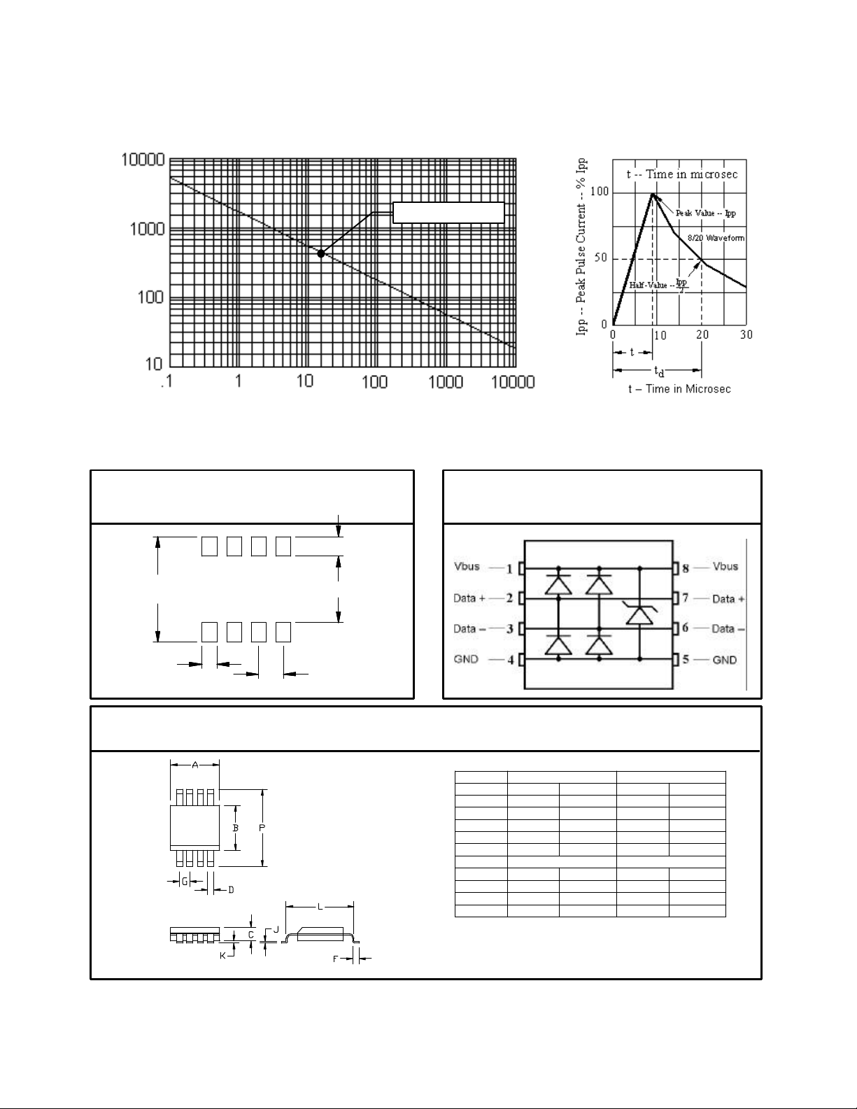
• Peak Pulse Power: 500 Watts (8/20 µsec, Figure 1
and 2)
• Pulse Repetition Rate: <.01%
ELECTRICAL CHARACTERISTICS PER LINE @ 250C Unless otherwise specified
STAND
OFF
VOLTAG
PART
NUMBER
USB6B1 USB6 5.0 6.0 9.8 18 5 15 3
DEVICE
MARKING
V
VOLTS
MAX MIN MAX MAX MAX TYP MAX
E
WM
BREAKDOWN
VOLTAGE
V
BR
@1 mA
VOLTS
CLAMPING
VOLTAGE
V
C
@ 1 Amp
(FIGURE 2)
VOLTS
CLAMPING
VOLTAGE
V
C
@ 5 Amp
(FIGURE 2)
VOLTS
STANDBY
CURRENT
I
D
@ V
WM
µA
CAPACITANCE
(f=1 MHz)
@0V
C
Data + To Data -
pF
TEMPERATURE
COEFFICIENT
of V
BR
á
V(BR)
mV/°C
MSC1068.PDF ISO 9001 CERTIFIED REV E 7/07/2000

INCHES
MILLIMETERS
MAX
MIN
DIM
MAX
MIN
0.197 A0.188
4.77
5.00
0.158
0.150
3.81
4.01
0.069
0.053
1.35
1.75
0.021
0.011
0.28
0.53
0.050
0.016
0.41
1.27
0.050 BSC
1.27 BSC
0.010
0.006
0.15
0.25
0.008
0.004
0.10
0.20
0.206
0.189
4.80
5.23 B C D F
G J K
L
0.244P0.228
5.79
6.19
– Peak Pulse Power - Watts
PP
P
Td - Pulse Time - µsec
Peak Pulse Power Vs Pulse Time
MOUNTING PAD S0-8 CIRCUIT DIAGRAM
WAVE FORMS
FIGURE 1
USB6B1
8/20 µs 500W Pulse
FIGURE 2
Pulse Wave Form
0.245
MIN
.030±.005
0.045±.005
.160±.005
.050 TYP
S0-8 PACKAGE
MSC1068.PDF ISO 9001 CERTIFIED REV E 7/07/2000
 Loading...