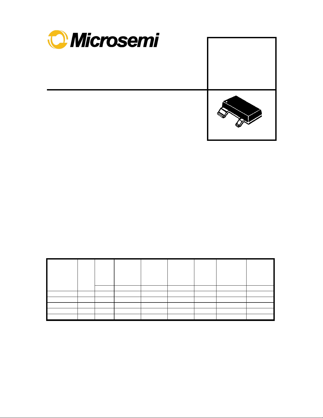
Microsemi USB0424C, USB0415C, USB0412C, USB0405C, USB0403C Datasheet

8700 E. Thomas Road
Scottsdale, AZ 85251
USB0403C
thru
Tel: (480) 941-6300
Fax: (480) 947-1503
USB0424C
TVSarray ™ Series
DESCRIPTION (300 watt)
This 4 pin 1 line bidirectional ULTRA LOW CAPACITANCE array is
designed for use in applications requiring board level protection from
voltage transients caused by electrostatic discharge (ESD) as defined
by IEC 1000-4-2, electrical fast transients (EFT) per IEC 1000-4-4 and
effects of secondary lightning.
These arrays are used to protect 1 discrete line utilizing pins (1,4 and
2,3). The S0T-143 product provides board level protection from static
electricity and other induced voltage surges that can damage sensitive
circuitry.
These TRANSIENT VOLTAGE SUPPRESSOR (TVS) Diode Arrays protect 3.3 Volt components such as
DRAM’s, SRAM’s, CMOS, HCMOS, HSIC, and low voltage interfaces up to 24Volts.
FEATURES MECHANICAL
• Protects 3.3 up through 24V Components • Molded SOT-143 Surface Mount
• Protects 1 line bidirectional • Weight: .035 grams (approximate)
• Provides electrically isolated protection • Body Marked with device marking
• SOT-143 Packaging code
• ULTRA LOW CAPACITANCE 5 pF • Pin #1 defined by DOT on top of
package
MAXIMUM RATINGS PACKAGING
• Operating Temperatures: -550C to +1500C • Tape & Reel EIA Standard 481-1-A
• Storage Temperature: -55
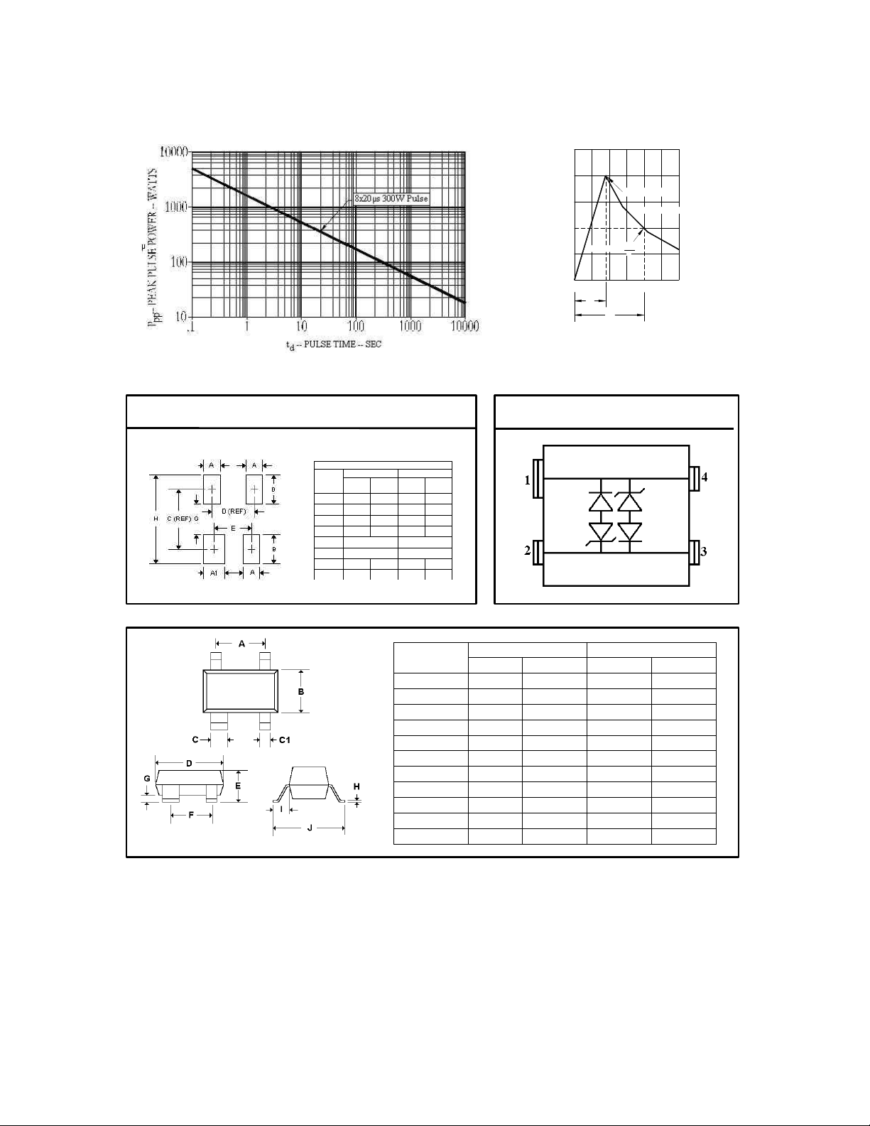
• Peak Pulse Power: 300 Watts (8/20 µsec, Figure 1)
• Pulse Repetition Rate: <.01%
ELECTRICAL CHARACTERISTICS @ 250C Unless otherwise specified
PART
NUMBER
USB0403C U3 3.3 4 8 11 200 5 -5
USB0405C U5 5.0 6.0 10.8 13 100 5 3
USB0412C U12 12.0 13.3 19 26 1 5 10
USB0415C U15 15.0 16.7 25 32 1 5 13
USB0424C U24 24.0 26.7 44 57 1 5 30
DEVICE
MARKING
NOTE: Transient Voltage Suppression (TVS) product is normally selected based on its stand off Voltage
VWM. Product selected voltage should be equal to or greater than the continuous peak operating voltage of
the circuit to be protected.
MSC0987.PDF ISO 9001 CERTIFIED REV D 1/14/2000
0
C to +1500C • 13 inch reel 10,000 pieces
STAND
VOLTAG
VOLTS
BREAKDOWN
OFF
E
V
WM
MAX MIN MAX MAX MAX MAX MAX
VOLTAGE
V
BR
@1 mA
VOLTS
CLAMPING
VOLTAGE
V
C
@ 1 Amp
(FIGURE 2)
VOLTS
CLAMPING
VOLTAGE
V
C
@ 5 Amp
(FIGURE 2)
VOLTS
STAND OFF
CURRENT
I
D
@ V
WM
µA
CAPACITANCE
(f=1 MHz)
@0V
C
pF
TEMPERATURE
COEFFICIENT
OF V
á
VBR
mV/°C
BR

USB0403C thru USB0424C
WAVE FORMS
100
Peak Value -- Ipp
8 X 20 Waveform
50
Ipp
Half-Value --
2
0
0
Ipp -- Peak Pulse Current -- % Ipp
t
t -- Time in microsec
10
t
20 30
d
FIGURE 1 FIGURE 2
Peak Pulse Power Vs Pulse Time Pulse Wave Form
MOUNTING PAD SOT 143 CIRCUIT DIAGRAM
DIMENSIONS
INCHES MM
DIM
MIN MAXMIN MA
A .032 .040 0.80 1.00
A1 .040 .048 1.00 1.20
B --- .057 --- 1.44
C --- .087 --- 2.20
D .075 BSC 1.90 BSC
E .067 BSC 1.70 BSC
G .032 .040 0.80 1.00
H .134 .140 3.40 3.60
X
DIMENSION
A 0.070 0.080 1.78 2.03
B 0.047 0.055 1.20 1.40
C 0.030 0.037 0.77 0.94
C1 0.015 0.020 0.37 0.50
D 0.110 0.119 2.80 3.04
E 0.035 0.044 0.89 1.17
F 0.071 0.079 1.80 2.00
G 0.0006 0.006 0.013 0.05
H 0.003 0.007 0.085 0.17
I 0.018 0.023 0.45 0.60
J 0.083 0.093 2.10 2.50
MSC0987.PDF ISO 9001 CERTIFIED REV D 1/14/2000
INCHES MILLIMETERS
MIN MAX MIN MAX
 Loading...