

DESCRIPTION KEY FEATURES
■■
■■
■ LOW START-UP CURRENT. (0.5mA max.)
■■
■■
■ TRIMMED OSCILLATOR DISCHARGE
CURRENT. (See Product Highlight)
p OPTIMIZED FOR OFF-LINE AND DC-TO-DC
CONVERTERS.
p AUTOMATIC FEED FORWARD
COMPENSATION.
p PULSE-BY-PULSE CURRENT LIMITING.
p ENHANCED LOAD RESPONSE
CHARACTERISTICS.
p UNDER-VOLTAGE LOCKOUT WITH
HYSTERESIS.
p DOUBLE PULSE SUPPRESSION.
p HIGH-CURRENT TOTEM POLE OUTPUT.
p INTERNALLY TRIMMED BANDGAP
REFERENCE.
p 500KHz OPERATION.
p LOW R
O
ERROR AMPLIFIER.
The UC184xA family of control ICs
provides all the necessary features to
implement off-line fixed-frequency,
current-mode switching power supplies
with a minimum of external components. The current mode architecture
demonstrates improved load regulation,
pulse-by-pulse current limiting and
inherent protection of the power supply
output switch. The IC includes: A
bandgap reference trimmed to ±1%
accuracy, an error amplifier, a current
sense comparator with internal clamp to
1V, a high current totem pole output
stage for fast switching of power
MOSFET's, and an externally programmable oscillator to set frequency and
maximum duty cycle. The undervoltage lock-out is designed to operate
with 250µA typ. start-up current,
allowing an efficient bootstrap supply
voltage design. Available options for
this family of products, such as start-up
voltage hysteresis and duty cycle, are
summarized below in the Available
Options section. The UC184xA family
of control ICs is also available in 14-pin
SOIC package which makes the Power
Output Stage Collector and Ground pins
available.
APPLICATIONS
■■
■■
■ ECONOMICAL OFF-LINE FLYBACK OR
FORWARD CONVERTERS.
■ DC-DC BUCK OR BOOST CONVERTERS.
■ LOW COST DC MOTOR CONTROL.
A VAILABLE OPTIONS
Part # Start-Up Hysteresis Max. Duty
Voltage Cycle
PACKAGE ORDER INFORMATION
T
A
(°C)
Plastic DIP
8-pin
0 to 70 UC384xAM UC384xADM UC384xAD —
-40 to 85 UC284xAM UC284xADM UC284xAD UC284xAY
-55 to 125 — — — UC184xAY
M
Plastic SOIC
8-pin
DM
Plastic SOIC
14-pin
D
Ceramic DIP
8-pin
Y
Note: All surface-mount packages are available in Tape & Reel. Append the letter "T" to part number. (i.e. UC3842ADMT)
UCx842A 16V 6V <100%
UCx843A 8.4V 0.8V <100%
UCx844A 16V 6V <50%
UCx845A 8.4V 0.8V <50%
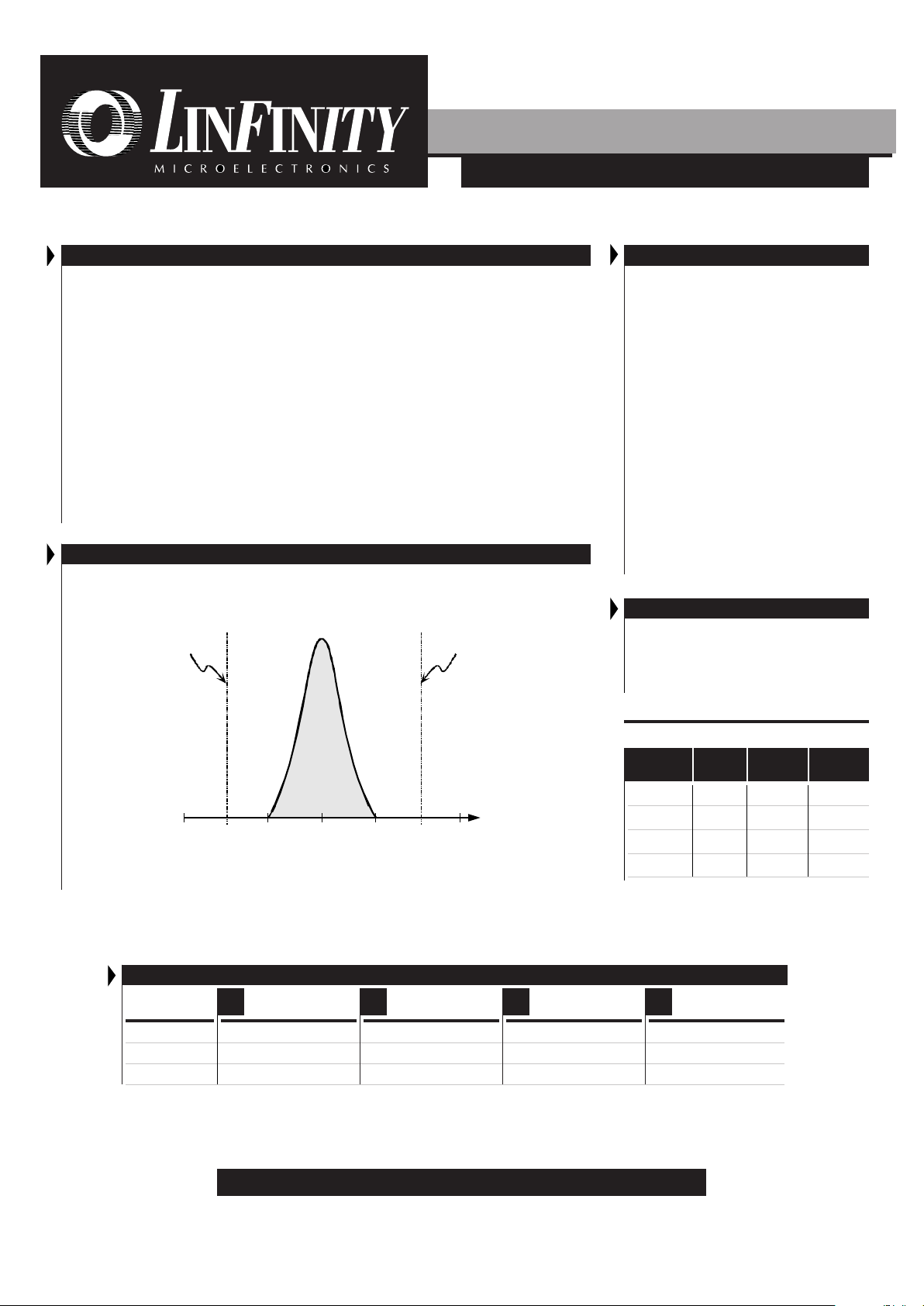
PRODUCT HIGHLIGHT
COMPARISON OF UC384XA VS. SG384X DISCHARGE CURRENT
UC384xA
7.5 8.3 9.3
Mean
SG384x
Min. Limit
7.8
−3σ
8.8
+3σ
SG384x
Max. Limit
Discharge Current Distribution - mA
T
A
=25°C
C URRENT MODE PWM CONTROLLER
P RODUCTION DATA SHEET
THE INFINITE POWER OF INNOVATION
Copyright © 1995
Rev. 1.2 12/95
FOR FURTHER INFORMATION CALL (714) 898-8121
11861 WESTERN AVENUE, GARDEN GROVE, CA. 92841
UC184xA/284xA/384xA
LIN DOC #:
1840
1
C URRENT MODE PWM CONTROLLER
UC184xA/284xA/384xA
PRODUCT DATABOOK 1996/1997
Copyright © 1995
Rev. 1.2 12/95
2
P
RODUCTION DATA SHEET
ABSOLUTE MAXIMUM RATINGS (Note 1)
Supply Voltage (Low Impedance Source) (VCC) ......................................................... 30V
Supply Voltage (I
CC
< 30mA).......................................................................... Self Limiting
Output Current ............................................................................................................. ±1A
Output Energy (Capacitive Load)................................................................................. 5µJ
Analog Inputs (V
FB
& I
SENSE
) ........................................................................ -0.3V to +6.3V
Error Amp Output Sink Current ............................................................................... 10mA
Power Dissipation at T
A
= 25°C (M Package) .............................................................. 1W
Storage Temperature Range .................................................................... -65°C to +150°C
Lead Temperature (Soldering, 10 Seconds) ............................................................. 300°C
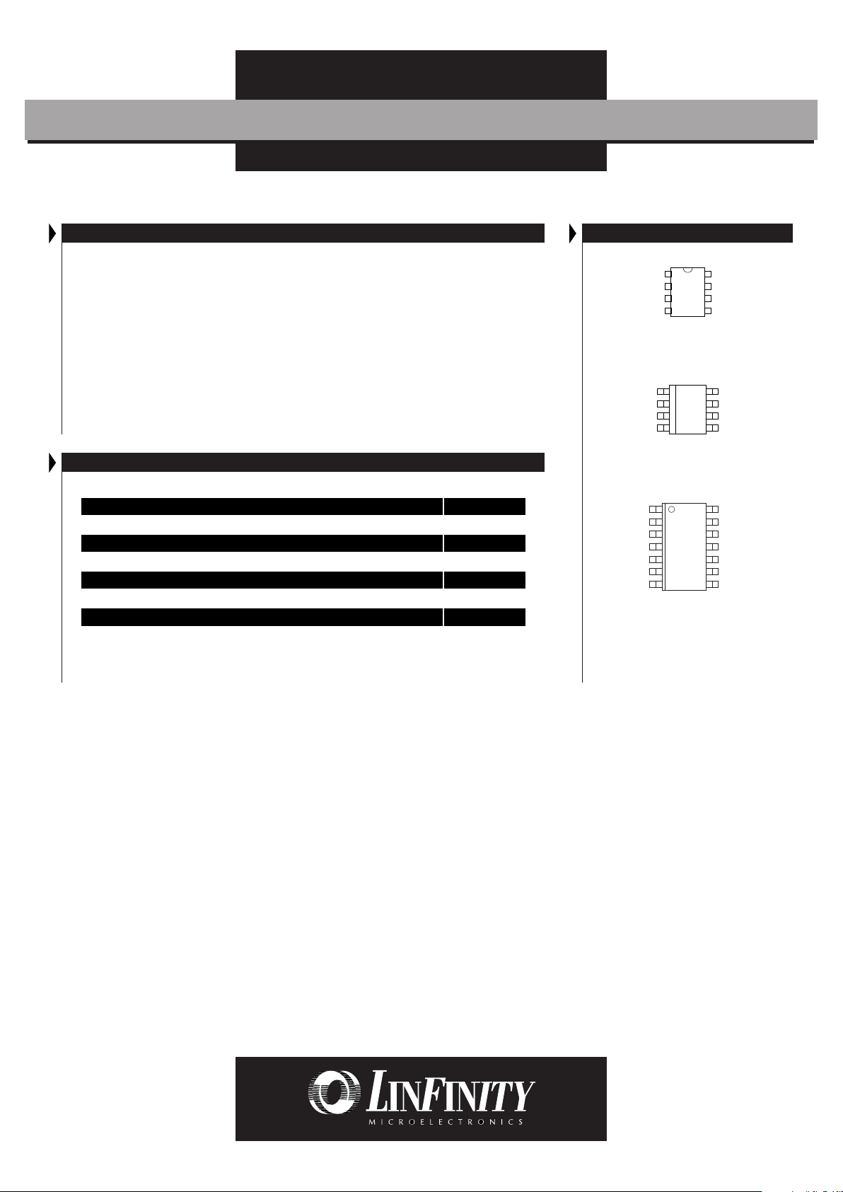
PACKAGE PIN OUTS
Note 1. Exceeding these ratings could cause damage to the device. All voltages are with respect
to Ground. Currents are positive into, negative out of the specified terminal. Pin
numbers refer to DIL packages only.
1 8
27
36
45
M & Y PACKAGE
(Top View)
M PACKAGE:
THERMAL RESISTANCE-JUNCTION TO AMBIENT,
θθ
θθ
θ
JA
95°C/W
DM PACKAGE:
THERMAL RESISTANCE-JUNCTION TO AMBIENT,
θθ
θθ
θ
JA
165°C/W
D PACKAGE:
THERMAL RESISTANCE-JUNCTION TO AMBIENT,
θθ
θθ
θ
JA
120°C/W
Y PACKAGE:
THERMAL RESISTANCE-JUNCTION TO AMBIENT,
θθ
θθ
θ
JA
130°C/W
Junction Temperature Calculation: T
J
= TA + (P
D
x θ
JA
).
The θ
JA
numbers are guidelines for the thermal performance of the device/pc-board system.
All of the above assume no ambient airflow
THERMAL DATA
DM PACKAGE
(Top View)
V
REF
V
CC
OUTPUT
GND
COMP
V
FB
I
SENSE
RT/C
T
1 8
27
36
45
V
REF
N.C.
V
CC
V
C
OUTPUT
GND
PWR GND
COMP
N.C.
V
FB
N.C.
I
SENSE
N.C.
RT/C
T
1 14
213
312
411
510
69
78
D PACKAGE
(Top View)
COMP
V
FB
I
SENSE
RT/C
T
V
REF
V
CC
OUTPUT
GND
C URRENT MODE PWM CONTROLLER
UC184xA/284xA/384xA
PRODUCT DATABOOK 1996/1997
3
Copyright © 1995
Rev. 1.2 12/95
P RODUCTION DATA SHEET
ELECTRICAL CHARACTERISTICS
(Unless otherwise specified, these specifications apply over the operating ambient temperatures for UC384xA with 0°C ≤ TA ≤ 70°C, UC284xA with -40°C ≤ TA ≤ 85°C,
UC184xA with -55°C ≤ T
A
≤ 125°C; V
CC
=15V; RT=10K; CT=3.3nF. Low duty cycle pulse testing techniques are used which maintains junction and case temperatures equal
to the ambient temperature.)
Reference Section
Parameter
Symbol
Test Conditions
Output Voltage V
REFTJ
= 25°C, IL = 1mA
Line Regulation 12 ≤ VIN ≤ 25V
Load Regulation 1 ≤ I
O
≤ 20mA
Temperature Stability (Note 2 & 7)
Total Output Variation Over Line, Load, and Temperature
Output Noise Voltage (Note 2) V
N
10Hz ≤ f ≤ 10kHz, TJ = 25°C
Long Term Stability (Note 2) TA = 125°C, t = 1000hrs
Output Short Circuit Current I
SC
UC384xA
Units
Min. Typ. Max. Min. Typ. Max.
UC184xA/284xA
4.95 5.00 5.05 4.90 5.00 5.10 V
620 620 mV
625 625 mV
0.2 0.4 0.2 0.4 mV/°C
4.9 5.1 4.82 5.18 V
50 50 µV
525 525 mV
-30 -100 -180 -30 -100 -180 mA
Oscillator Section
Initial Accuracy (Note 6) TJ = 25°C
Voltage Stability 12 ≤ VCC ≤ 25V
Temperature Stability (Note 2) T
MIN
≤ TA ≤ T
MAX
Amplitude (Note 2)
Discharge Current TJ = 25°C, V
PIN 4
= 2V
V
PIN 4
= 2V, T
MIN
≤ TA ≤ T
MAX
47 52 57 47 52 57 kHz
0.2 1 0.2 1 %
55%
1.7 1.7 V
7.8 8.3 8.8 7.8 8.3 8.8 mA
7.5 8.8 7.6 8.8 mA
Output Low Level
V
OL
I
SINK
= 20mA
I
SINK
= 200mA
Output High Level
V
OH
I
SOURCE
= 20mA
I
SOURCE
= 200mA
Rise Time (Note 2) T
R
TJ = 25°C, CL = 1nF
Fall Time (Note 2) T
F
TJ = 25°C, CL = 1nF
UVLO Saturation V
SATVCC
= 5V, I
SINK
= 10mA
Current Sense Section
Gain (Note 3 & 4) A
VOL
Maximum Input Signal (Note 3) V
PIN 1
= 5V
Power Supply Rejection Ratio (Note 3) PSRR 12 ≤ V
CC
≤ 25V
Input Bias Current I
B
Delay to Output (Note 2) T
pdVPIN 3
= 0 to 2V
Output Section
2.85 3 3.15 2.85 3 3.15 V/V
0.9 1 1.1 0.9 1 1.1 V
70 70 dB
-2 -10 -2 -10 µA
150 300 150 300 ns
0.1 0.4 0.1 0.4 V
1.5 2.2 1.5 2.2 V
13 13.5 13 13.5 V
12 13.5 12 13.5 V
50 150 50 150 ns
50 150 50 150 ns
0.7 1.2 0.7 1.2 V
(Electrical Characteristics continue next page.)
Error Amp Section
Input Voltage V
PIN 1
= 2.5V
Input Bias Current I
B
Open Loop Gain A
VOL
2 ≤ VO ≤ 4V
Unity Gain Bandwidth (Note 2) UGBW T
j
= 25°C
Power Supply Rejection Ratio (Note 3) PSRR 12 ≤ VCC ≤ 25V
Output Sink Current I
OLVPIN 2
= 2.7V, V
PIN 1
= 1.1V
Output Source Current I
OHVPIN 2
= 2.3V, V
PIN 1
= 5V
Output Voltage High Level V
OHVPIN 2
= 2.3V, RL = 15K to ground
Output Voltage Low Level V
OLVPIN 2
= 2.7V, RL = 15K to V
REF
2.45 2.50 2.55 2.42 2.50 2.58 V
-0.3 -1 -0.3 -2 µA
65 90 65 90 dB
0.7 1 0.7 1 MHz
60 70 60 70 dB
26 26 mA
-0.5 -0.8 -0.5 -0.8 mA
56 56 V
0.7 1.1 0.7 1.1 V

C URRENT MODE PWM CONTROLLER
UC184xA/284xA/384xA
PRODUCT DATABOOK 1996/1997
Copyright © 1995
Rev. 1.2 12/95
4
P
RODUCTION DATA SHEET
ELECTRICAL CHARACTERISTICS (Con't.)
Under-Voltage Lockout Section
Parameter
Symbol
Test Conditions
Start Threshold x842A/4A
x843A/5A
Min. Operation Voltage After Turn-On x842A/4A
x843A/5A
UC384xA
Units
Min. Typ. Max. Min. Typ. Max.
UC184xA/284xA
15 16 17 14.5 16 17.5 V
7.8 8.4 9.0 7.8 8.4 9.0 V
9 10 11 8.5 10 11.5 V
7.0 7.6 8.2 7.0 7.6 8.2 V
PWM Section
Maximum Duty Cycle x842A/3A
x844A/5A
Minimum Duty Cycle
94 96 100 94 96 100 %
47 48 50 47 48 50 %
00%
Total Standby Section
Start-Up Current
Operating Supply Current I
CC
Zener Voltage VZICC = 25mA
0.3 0.5 0.3 0.5 mA
11 17 11 17 mA
30 35 30 35 V
BLOCK DIAGRAM
*
- V
CC
and VC are internally connected for 8 pin packages.
**
- POWER GROUND and GROUND are internally connected for 8 pin packages.
***
- Toggle flip flop used only in x844A and x845A series.
Notes: 2. These parameters, although guaranteed, are not 100% tested in
production.
3. Parameter measured at trip point of latch with V
VFB
= 0.
4. Gain defined as: A
VOL
= ; 0 ≤ V
ISENSE
≤ 0.8V.
5. Adjust VCC above the start threshold before setting at 15V.
6. Output frequency equals oscillator frequency for the UC1842A
and UC1843A. Output frequency is one half oscillator frequency
for the UC1844A and UC1845A.
7. "Temperature stability, sometimes referred to as average temperature
coefficient, is described by the equation:
Temp Stability =
V
REF
(max.) & V
REF
(min.) are the maximum & minimum reference
voltage measured over the appropriate temperature range. Note that
the extremes in voltage do not necessarily occur at the extremes in
temperature."
V
REF
(max.) - V
REF
(min.)
TJ (max.) - TJ (min.)
∆ V
COMP
∆ V
ISENSE
UVLO
S / R
5V
Ref
Internal
Bias
34V
Error Amp
1V
Current Sense
Comparator
PWM
Latch
S
R
R
Oscillator
2R
**
T***
V
REF
Good Logic
2.5V
UVLO
16V (1842A/4A)
8.4V (1843A/5A)
Hysteresis
6V (1842A/4A)
0.8V (1843A/5A)
COMP
CURRENT SENSE
V
FB
RT/C
T
GROUND
*
V
CC
V
REF
5.0V
50mA
V
C
*
OUTPUT
POWER GROUND
**

C URRENT MODE PWM CONTROLLER
UC184xA/284xA/384xA
PRODUCT DATABOOK 1996/1997
5
Copyright © 1995
Rev. 1.2 12/95
P RODUCTION DATA SHEET
CHARACTERISTIC CURVES
FIGURE 1. — OSCILLATOR FREQUENCY vs. TIMING
RESISTOR
300 3.0k 100
k
0
100k
RT - (ohms)
Oscillator Frequency - (Hz)
10k
1M
1.0k 10.0k 30.0k
CT = 1nF
CT = 2.2nF
CT = 4.7nF
FIGURE 2. — MAXIMUM DUTY CYCLE vs. TIMING RESISTOR
300 3.0k 100
k
0
40.0
RT - (ohms)
Maximum Duty Cycle - (%)
20.0
60.0
1.0k 10.0k 30.0k
80.0
100.0
Note: Output drive frequency is half the oscillator frequency for
the UCx844A/5A devices.
8
4
5
V
REF
RT/C
T
GROUND
R
T
C
T
For R
T
> 5k, f »
1.72
R
T CT

C URRENT MODE PWM CONTROLLER
UC184xA/284xA/384xA
PRODUCT DATABOOK 1996/1997
Copyright © 1995
Rev. 1.2 12/95
6
P
RODUCTION DATA SHEET
TYPICAL APPLICATION CIRCUITS
FIGURE 3. — CURRENT SENSE SPIKE SUPPRESSION
FIGURE 4. — MOSFET PARASITIC OSCILLATIONS
6
Q1
V
CC
DC BUS
5
R
S
R
1
UCx84xA
7
UCx84xA
3
5
6
7
R
S
C
Q1
V
CC
DC BUS
I
PK
I
PK(MAX)
=
1.0V
R
S
CHANGE
FIGURE 5. — EXTERNAL DUTY CYCLE CLAMP AND MULTI-UNIT SYNCHRONIZATION
A resistor (R1) in series with the MOSFET gate will reduce overshoot
& ringing caused by the MOSFET input capacitance and any
inductance in series with the gate drive. (Note: It is very important to
have a low inductance ground path to insure correct operation of the
I.C. This can be done by making the ground paths as short and as
wide as possible.)
The RC low pass filter will eliminate the leading edge current spike
caused by parasitics of Power MOSFET.
f =
(RA + 2RB)C
1.44
f =
RA + 2R
B
R
B Precision duty cycle limiting as well as synchronizing several parts is
possible with the above circuitry.
2
6
7
R
B
R
A
5 1
84
3
555
TIMER
4
5
8
To other
UCx84xA devices
0.01
UCx84xA

C URRENT MODE PWM CONTROLLER
UC184xA/284xA/384xA
PRODUCT DATABOOK 1996/1997
7
Copyright © 1995
Rev. 1.2 12/95
P RODUCTION DATA SHEET
TYPICAL APPLICATION CIRCUITS (continued)
FIGURE 6. — SLOPE COMPENSATION
FIGURE 7. — OPEN LOOP LABORATORY FIXTURE
2
3
4
8
7
6
5
COMP
V
FB
I
SENSE
RTC
T
V
REF
V
CC
OUTPUT
GROUND
0.1µF 0.1µF
A
UCx84xA
R
T
2N2222
100K
4.7K
1K
4.7K
5K
I
SENSE
ADJUST
ERROR AMP
A
DJUST
C
T
1K
GROUND
OUTPUT
V
CC
V
REF
1
OSCILLATOR
V
REF
GOOD LOGIC
S
R5VREF
INTERNAL
BIAS
8(14)
4(7)
2(3)
1(1)
R
F
C
F
R
d
R
i
From V
O
R
SLOPE
2N222A
R
T
5V
UVLO
2.5V
ERROR
AMP
C
T
1V
2R
R
C.S.
COMP
PWM
LATCH
5(9)
3(5)
5(8)
CR
S
R
6(10)
7(11)
7(12)
V
CC
DC BUS
V
O
Q1
UCx84xA
Due to inherent instability of current mode converters running above 50% duty cycle, slope compensation should be added to either
the current sense pin or the error amplifier. Figure 6 shows a typical slope compensation technique.
High peak currents associated with capacitive loads necessitate careful grounding techniques. Timing and bypass capacitors should be
connected to pin 5 in a single point ground. The transistor and 5k potentiometer are used to sample the oscillator waveform and apply an
adjustable ramp to pin 3.

C URRENT MODE PWM CONTROLLER
UC184xA/284xA/384xA
PRODUCT DATABOOK 1996/1997
Copyright © 1995
Rev. 1.2 12/95
8
P
RODUCTION DATA SHEET
TYPICAL APPLICATION CIRCUITS (continued)
FIGURE 8. — OFF-LINE FLYBACK REGULATOR
SPECIFICATIONS
Input line voltage: 90VAC to 130VAC
Input frequency: 50 or 60Hz
Switching frequency: 40KHz ±10%
Output power: 25W maximum
Output voltage: 5V +5%
Output current: 2 to 5A
Line regulation: 0.01%/V
Load regulation: 8%/A*
Efficiency @ 25 Watts,
V
IN
= 90VAC: 70%
V
IN
= 130VAC: 65%
Output short-circuit current: 2.5Amp average
* This circuit uses a low-cost feedback scheme in which the DC
voltage developed from the primary-side control winding is
sensed by the UC3844A error amplifier. Load regulation is
therefore dependent on the coupling between secondary and
control windings, and on transformer leakage inductance.
7
150kW
100pF
V
FB
COMP
V
REF
RT/C
T
4700µF
10V
5V
2-5A
ISOLATION
BOUNDARY
3600pF
400V
1N4935
820pF
2.5k
W
1N4935
IRF830
27k
W
0.01µF
10µF
20V
1N4935
1k
W
470pF
0.85k
W
MBR735TI
4.7k
W
2W
140kW
1/2W
220µF
250V
4.7kW 1W
1N4004
1N40041N4004
1N4004
AC
INPUT
V
CC
OUT
CUR
SEN
GND
UC3844A
20kW
3.6k
W
10kW
.0022µF0.01µF
16V
3
6
2
1
8
4
5
 Loading...