Microsemi Corporation SMDA05, SMDA03C, SMDA05C, SMDA03, SMDA12 Datasheet
...
8700 E. Thomas Road
Scottsdale, AZ 85251
Tel: (480) 941-6300
Fax: (480) 947-1503
SMDA/B03
thru
SMDA/B24C
DESCRIPTION (300 and 500 watt)
This 8 pin 4 line Unidirectional or Bidirectional array is designed for use in
applications where protection is required at the board level from voltage transients
caused by electrostatic discharge (ESD) as defined by IEC 1000-4-2, electrical fast
transients (EFT) per IEC 1000-4-4 and effects of secondary lighting.
These arrays are used to protect any combination of 4 lines. The SMDA/B product
provides board level protection from static electricity and other induced voltage
surges that can damage sensitive circuitry.
These TRANSIENT VOLTAGE SUPPRESSOR (TVS) Diode Arrays protect 3.0/3.3
Volt components such as DRAM’s, SRAM’s, CMOS, HCMOS, HSIC, and low
voltage interfaces up to 24Volts.
FEATURES MECHANICAL
• Protects 3.0/3.3 up through 24V Components • Molded SO-8 Surface Mount
• Protects 4 lines Unidirectional or Bidirectional • Weight: 0.066 grams (approximate)
• Provides electrically isolated protection • Body Marked with Logo, and device number
• SO-8 Packaging • Pin #1 defined by DOT on top of package
MAXIMUM RATINGS PACKAGING
• Operating Temperatures: -550C to +1500C • Tape & Reel EIA Standard 481-1-A
• Storage Temperature: -550C to +1500C • 13 inch reel 2,500 pieces (OPTIONAL)
• SMDA Peak Pulse Power: 300 Watts (8/20 µsec, Figure 1) • Carrier tubes 95 pcs per (STANDARD)
• SMDB Peak Pulse Power: 500 Watts (8/20 µsec, Figure 1)
• Pulse Repetition Rate: <.01%
TVSarray Series
ELECTRICAL CHARACTERISTICS PER LINE @ 250C Unless otherwise specified
WM
BREAKDOW
N
VOLTAGE
V
BR
@1 mA
VOLTS
CLAMPING
VOLTAGE
V
C
@ 1 Amp
(FIGURE 2)
VOLTS
CLAMPING
VOLTAGE
V
C
@5 Amp
(FIGURE2)
VOLTS
LEAKAGE
CURRENT
I
D
@ V
WM
µA
CAPACITANCE
(f=1 MHz)
@0V
C
pF
TEMPERATURE
COEFFICIENT
STAND
OFF
PART
NUMBER
SMDA03 SDK 3.3 4 7 9 200 800 -3
SMDA03C SDL 3.3 4 7 9 200 400 -5
SMDB03 PDK 3.3 4 7 9 200 800 -3
SMDB03C PDL 3.3 4 7 9 200 400 -5
SMDA05 SDA 5.0 6 9.8 11 20 600 3
SMDA05C SDB 5.0 6 9.8 11 40 300 1
SMDB05 PDA 5.0 6 9.8 11 20 600 3
SMDB05C PDB 5.0 6 9.8 11 40 300 1
SMDA12 SDC 12.0 13.3 19 24 1 185 10
SMDA12C SDD 12.0 13.3 19 24 1 94 8
SMDB12 PDC 12.0 13.3 19 24 1 185 10
SMDB12C PDD 12.0 13.3 19 24 1 94 8
SMDA15 SDE 15.0 16.7 24 30 1 140 13
SMDA15C SDF 15.0 16.7 24 30 1 70 11
SMDB15 PDE 15.0 16.7 24 30 1 140 13
SMDB15C PDF 15.0 16.7 24 30 1 70 11
SMDA24 SDG 24.0 26.7 43 55 1 90 30
SMDA24C SDH 24.0 26.7 43 55 1 45 28
SMDB24 PDG 24.0 26.7 43 55 1 90 30
SMDB24C PDH 24.0 26.7 43 55 1 45 28
DEVICE
MARKING
VOLTAGE
V
VOLTS
MAX MIN MAX MAX MAX TYP MAX
Part numbers with a “C” suffix are bidirectional devices
OF V
Mv/°C
BR
á
VBR
MSC0330A.PDF ISO 9001 CERTIFIED REV N 7/06/2000

SMDA/B03 thru SMDA/B24C
INCHES
MILLIMETERS
MAX
MIN
DIM
MAX
MIN
0.197 A0.188
4.77
5.00
0.158
0.150
3.81
4.01
0.069
0.053
1.35
1.75
0.021
0.011
0.28
0.53
0.050
0.016
0.41
1.27
0.050 BSC
1.27 BSC
0.010
0.006
0.15
0.25
0.008
0.004
0.10
0.20
0.206
0.189
4.80
5.23 B C D F
G J K
L
0.244P0.228
5.79
6.19
NOTE: Transient Voltage Suppression (TVS) product is normally selected based on its stand off Voltage VWM. Product
selected voltage should be equal to or greater than the continuous peak operating voltage of the circuit to be protected.
WAVE FORMS
Ip
100
p -
Pe
ak
Pu
50
lse
Cu
rre
nt
0
--
0 10 20 30
%
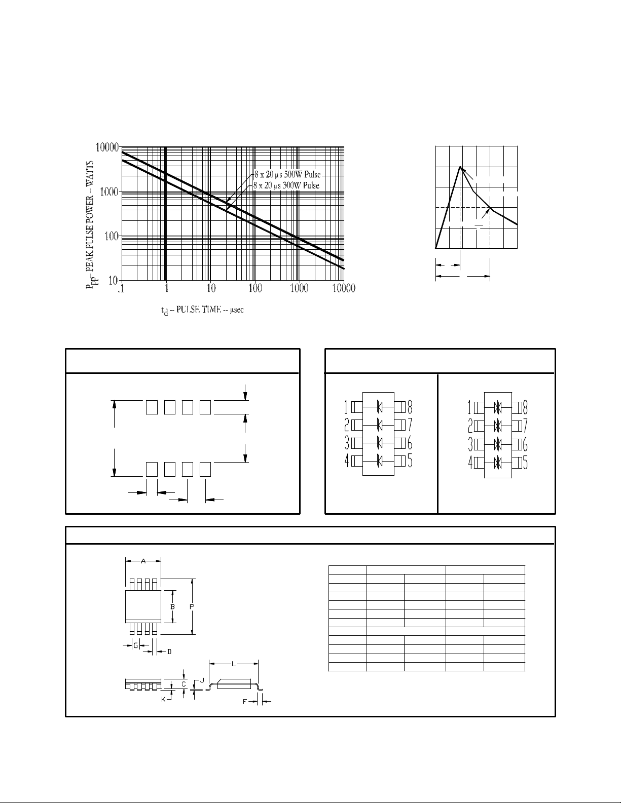
FIGURE 1 FIGURE 2
Peak Pulse Power Vs Pulse Time Pulse Wave Form
Peak Value -- Ipp
8 X 20 Waveform
Ipp
Half-Value --
2
t
t
d
t -- Time in microsec
0.245
MIN
.030±.005
MOUNTING PAD SO-8 CIRCUIT DIAGRAM
0.045±.005
.160±.005
.050 TYP
UNIDIRECTIONAL BIDIRECTIONAL
SO-8 PACKAGE
MSC0330A.PDF ISO 9001 CERTIFIED REV N 7/06/2000
 Loading...