Microsemi SMCG5629, SMCG5665A, SMCJ5629, SMCJ5665A Technical data

查询SMCG5629供应商
and SMCJ5629 thru SMCJ5665A
Transient Voltage Suppressors
SCOTTSDALE DIVISION
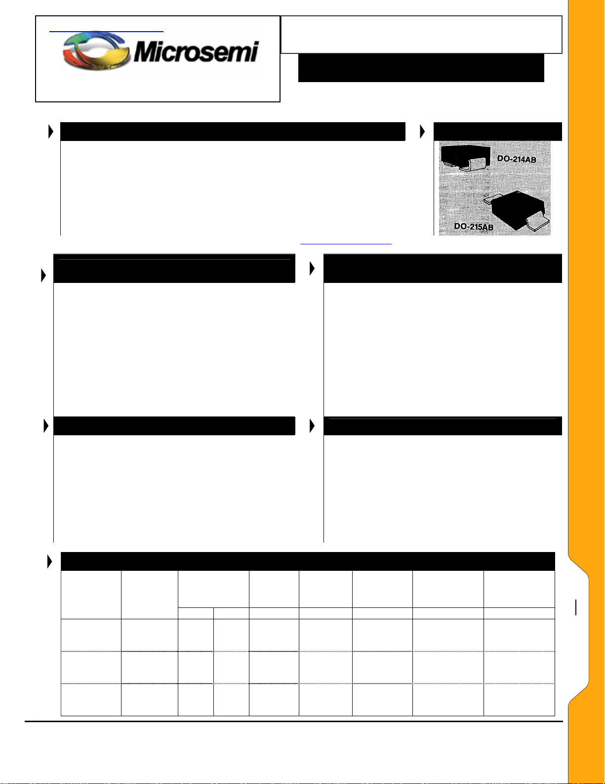
These surface mount Transient Voltage Suppressors (TVSs) are used for protecting
sensitive components requiring low clamping voltage levels. They are rated at high
current impulses typically generated by inductive switching transients. Other
benefits are achieved with low-profile surface mount J-bend or Gull-wing terminals
for stress-relief and lower weight. Its low-flat profile provides easier insertion or
automatic handling benefits compared to other MELF style packages. Options for
screening similar to JAN, JANTX, JANTXV, and JANS also exist by using MQ, MX,
MV or MSP respectively for part number prefixes and high reliability screening in
accordance with MIL-PRF-19500/507.
IMPORTANT: For the most current data, consult MICROSEMI’s website: http://www.microsemi.com
FEATURES
• Working Standoff Voltages: 5.5 volts to 171 volts
• Metallurgically bonded
• Reliability data per JESD22-A108, JESD22-A104,
JESD22-A113-B, JESD22-A101-B, and JESD22-A102
• Thermally efficient surface mount with J-bends or
Gull wings termination for stress relief (flat handling
surface and easier placement)
• Options for screening in accordance with MIL-PRF-
19500/500 for JAN, JANTX, JANTXV, and JANS are
available by adding MQ, MX, MV, or MSP prefixes
respectively to part numbers. For example,
designate a MXSMCJ5629A for a JANTX screen.
• Operating temperature: -55°C to +150°C
• Storage temperature: -55°C to +150°C
• 1500 Watts of Peak Pulse Power at 10/1000 µs as
shown in Figure 3 (see Figure 1 for other t
• Thermal resistance, R
• Impulse repetition rate (duty factor): 0.01%
• 5.0 Watt steady-state maximum power at T
• t
clamping
(theoretical)
• Forward voltage V
ELECTRICAL CHARACTERISTICS @ 25oC (Test Both Polarities)
MICROSEMI
Part Number
Modified
“G”
Bend Lead
SMCG5629
SMCG5629A
SMCG5630
SMCG5630A
SMCG5631
SMCG5631A
SMCG5632
SMCG5632A
SMCG5633
SMCG5633A
SMCG5634
SMCG5634A
MAXIMUM RATINGS
θJL
(0V to V
min): 50 picoseconds max
(BR)
@ 100 Amps 8.3 ms: 3.5 V max.
F
MICROSEMI
Part Number
Modified
“J”
Bend Lead
SMCJ5629
SMCJ5629A
SMCJ5630
SMCJ5630A
SMCJ5631
SMCJ5631A
SMCJ5632
SMCJ5632A
SMCJ5633
SMCJ5633A
SMCJ5634
SMCJ5634A
DESCRIPTION
• For high reliability transient voltage suppression in
• Light weight for airborne or satellite applications
• Superior surge quality to protect from ESD and EFT
• Lightning surge protection per IEC61000-4-5 for
APPLICATIONS / BENEFITS
low profile surface mount locations requiring easy
placement and strain relief
transients per IEC61000-4-2 and -4-4
Class 1 and 2 with source impedance of 42 Ohms as
well as Class 3 and 4 selectively at lower voltages
(V
) and higher surge current (IPP) ratings herein
WM
• Protects sensitive components such as ICs, CMOS,
Bipolar, BiCMOS, ECL, DTL, T
values)
)
BR
7.48
7.14
8.25
7.88
9.02
8.61
10.0
9.55
11.0
10.5
12.1
11.6
P
=25°C
L
Test
Current
)
(I
(BR)
10
10
10
10
10
10
1
1
1
1
1
1
Rated
Standoff
Voltage
(V
WM
5.50
5.80
6.05
6.40
6.63
7.02
7.37
7.78
8.10
8.55
8.92
9.40
= 20°C/W
Breakdown
Voltage*
(V
MIN. MAX.
Vdc Vdc mAdc V µAdc V A
6.12
6.45
6.75
7.13
7.38
7.79
8.19
8.65
9.00
9.5
9.9
10.5
MECHANICAL AND PACKAGING
• Molded epoxy package meets UL94V-0
• Terminals: Solderable per MIL-STD-750
Method 2026. (max 260 °C for 10 sec.)
• Body marked with P/N without SMCJ or SMCG letters
(ie. 5629A, 5640, 5655A, 5662, 5665A, etc.)
• Cathode indicated by band
• Weight: 0.25 grams (approximate)
• Tape & Reel packaging per EIA-481
(2500 units/reel)
Maximum
Standby
)
Current
at VWM)
(I
D
1000
1000
500
500
200
200
50
50
10
10
SMCG5629 thru SMCG5665A
Maximum Peak
Reverse Voltage
(V
C
5
5
APPEARANCE
2
L, etc.
max. at IPP)
10.8
10.5
11.7
11.3
12.5
12.1
13.8
13.4
15.0
14.5
16.2
15.6
Maximum Peak
Pulse Current
(IPP)
139
143
128
132
120
124
109
112
100
103
93
96
WWW.Microsemi . COM
SMCG/J5629 thru
SMCG/J5665A
Copyright 2003
01-24-2003 REV A
Microsemi
Scottsdale Division
8700 E. Thomas Rd. PO Box 1390, Scottsdale, AZ 85252 USA, (480) 941-6300, Fax: (480) 947-1503
Page 1

SCOTTSDALE DIVISION
SMCG5629 thru SMCG5665A
and SMCJ5629 thru SMCJ5665A
Transient Voltage Suppressors
* V
MICROSEMI
Part Number
Modified
“G”
Bend Lead
SMCG5635
SMCG5635A
SMCG5636
SMCG5636A
SMCG5637
SMCG5637A
SMCG5638
SMCG5638A
SMCG5639
SMCG5639A
SMCG5640
SMCG5640A
SMCG5641
SMCG5641A
SMCG5642
SMCG5642A
SMCG5643
SMCG5643A
SMCG5644
SMCG5644A
SMCG5645
SMCG5645A
SMCG5646
SMCG5646A
SMCG5647
SMCG5647A
SMCG5648
SMCG5648A
SMCG5649
SMCG5649A
SMCG5650
SMCG5650A
SMCG5651
SMCG5651A
SMCG5652
SMCG5652A
SMCG5653
SMCG5653A
SMCG5654
SMCG5654A
SMCG5655
SMCG5655A
SMCG5656
SMCG5656A
SMCG5657
SMCG5657A
SMCG5658
SMCG5658A
SMCG5659
SMCG5659A
SMCG5660
SMCG5660A
SMCG5661
SMCG5661A
SMCG5662
SMCG5662A
SMCG5663
SMCG5663A
SMCG5664
SMCG5664A
SMCG5665
SMCG5665A
NOTE 1: A TVS is normally selected according to the rated “Stand Off Voltage” VWM which should be equal to or greater than the dc or continuous peak
operating voltage level.
is measured after I
(BR)
MICROSEMI
Part Number
Modified
“J”
Bend Lead
SMCJ5635
SMCJ5635A
SMCJ5636
SMCJ5636A
SMCJ5637
SMCJ5637A
SMCJ5638
SMCJ5638A
SMCJ5639
SMCJ5639A
SMCJ5640
SMCJ5640A
SMCJ5641
SMCJ5641A
SMCJ5642
SMCJ5642A
SMCJ5643
SMCJ5643A
SMCJ5644
SMCJ5644A
SMCJ5645
SMCJ5645A
SMCJ5646
SMCJ5646A
SMCJ5647
SMCJ5647A
SMCJ5648
SMCJ5648A
SMCJ5649
SMCJ5649A
SMCJ5650
SMCJ5650A
SMCJ5651
SMCJ5651A
SMCJ5652
SMCJ5652A
SMCJ5653
SMCJ5653A
SMCJ5654
SMCJ5654A
SMCJ5655
SMCJ5655A
SMCJ5656
SMCJ5656A
SMCJ5657
SMCJ5657A
SMCJ5658
SMCJ5658A
SMCJ5659
SMCJ5659A
SMCJ5660
SMCJ5660A
SMCJ5661
SMCJ5661A
SMCJ5662
SMCJ5662A
SMCJ5663
SMCJ5663A
SMCJ5664
SMCJ5664A
SMCJ5665
SMCJ5665A
(BR)
Breakdown
Voltage*
)
(V
BR
MIN. MAX.
Test
Current
)
(I
(BR)
Rated
Standoff
Voltage
)
(V
WM
Maximum
Standby
Current
at VWM)
(I
D
Maximum Peak
Reverse Voltage
(VC max. at IPP)
Maximum Peak
Pulse Current
Vdc Vdc mAdc V µAdc V A
10.8
11.4
11.7
12.4
13.5
14.3
14.4
15.2
16.2
17.1
18.0
19.0
19.8
20.9
21.6
22.8
24.3
25.7
27.0
28.5
29.7
31.4
32.4
34.2
35.1
37.1
38.7
40.9
42.3
44.7
45.9
48.5
50.4
53.2
55.8
58.9
61.2
64.6
67.5
71.3
73.8
77.9
81.9
86.5
90
95
99
105
108
114
117
124
135
143
144
152
153
162
162
171
180
190
has been applied for < 300 ms. No suffix is 10% tolerance and suffix A is 5% tolerance for V
13.2
12.6
14.3
13.7
16.5
15.8
17.6
16.8
19.8
18.9
22.0
21.0
24.2
23.1
26.4
25.2
29.7
28.4
33.0
31.5
36.3
34.7
39.6
37.8
42.9
41.0
47.3
45.2
51.7
49.4
56.1
53.6
61.6
58.8
68.2
65.1
74.8
71.4
82.5
78.8
90.2
86.1
100.0
95.5
110
105
121
116
132
126
143
137
165
158
176
168
187
179
198
189
220
210
1
1
10.2
1
10.5
1
11.1
1
12.1
1
12.8
1
12.9
1
13.6
1
14.5
1
15.3
1
16.2
1
17.1
1
17.8
1
18.8
1
19.4
1
20.5
1
21.8
1
23.1
1
24.3
1
25.6
1
26.8
1
28.2
1
29.1
1
30.8
1
31.6
1
33.3
1
34.8
1
36.8
1
38.1
1
40.2
1
41.3
1
43.6
1
45.4
1
47.8
1
50.2
1
53.0
1
55.1
1
58.1
1
60.7
1
64.1
1
66.4
1
70.1
1
73.7
1
77.8
1
81.0
1
85.5
1
89.2
1
94.0
1
97.2
1
102
1
105
1
111
1
121
1
128
1
130
1
136
1
138
1
145
1
146
1
154
1 1 162
171
9.72
5
5
5
5
5
5
5
5
5
5
5
5
5
5
5
5
5
5
5
5
5
5
5
5
5
5
5
5
5
5
5
5
5
5
5
5
5
5
5
5
5
5
5
5
5
5
5
5
5
5
5
5
5
5
5
5
5
5
5
5
5
5
17.3
16.7
19.0
18.2
22.0
21.2
23.5
22.5
26.5
25.2
29.1
27.7
31.9
30.6
34.7
33.2
39.1
37.5
43.5
41.4
47.7
45.7
52.0
49.9
56.4
53.9
61.9
59.3
67.8
64.8
73.5
70.1
80.5
77.0
89.0
85.0
98.0
92.0
108
103
118
113
131
125
144
137
158
152
173
165
187
179
215
207
230
219
244
234
258
246
287
274
87
90
79
82
68
71
64
67
56.5
59.5
51.5
54
47
49
43
45
38.5
40
34.5
36
31.5
33
29
30
26.5
28
24
25.3
22.2
23.2
20.4
21.4
18.6
19.5
16.9
17.7
15.3
16.3
13.9
14.6
12.7
13.3
11.4
12.0
10.4
11.0
9.5
9.9
8.7
9.1
8.0
8.4
7.0
7.2
6.5
6.8
6.2
6.4
5.8
6.1
5.2
5.5
.
(BR)
(IPP)
WWW.Microsemi . COM
SMCG/J5629 thru
SMCG/J
5665A
Copyright 2003
01-24-2003 REV A
Microsemi
Scottsdale Division
8700 E. Thomas Rd. PO Box 1390, Scottsdale, AZ 85252 USA, (480) 941-6300, Fax: (480) 947-1503
Page 2
 Loading...