

Page 1

SmartFusion Development Kit
User’s Guide
Page 2

SmartFusion Development Kit
Table of Contents
Introduction . . . . . . . . . . . . . . . . . . . . . . . . . . . . . . . . . . . . . . . . . . . . . . . . . . . . . . . . . . . . . . . . . . . . . . 5
Kit Contents . . . . . . . . . . . . . . . . . . . . . . . . . . . . . . . . . . . . . . . . . . . . . . . . . . . . . . . . . . . . . . . . . . . . . . . . . . . . . . . 6
SmartFusion Development Kit Web Resources . . . . . . . . . . . . . . . . . . . . . . . . . . . . . . . . . . . . . . . . . . . . . . . . . . . . 6
Board Description . . . . . . . . . . . . . . . . . . . . . . . . . . . . . . . . . . . . . . . . . . . . . . . . . . . . . . . . . . . . . . . . . . . . . . . . . . 6
1 Installation and Settings. . . . . . . . . . . . . . . . . . . . . . . . . . . . . . . . . . . . . . . . . . . . . . . . . . . . . . . . . . . . . 9
Software Installation . . . . . . . . . . . . . . . . . . . . . . . . . . . . . . . . . . . . . . . . . . . . . . . . . . . . . . . . . . . . . . . . . . . . . . . . . 9
Hardware Installation . . . . . . . . . . . . . . . . . . . . . . . . . . . . . . . . . . . . . . . . . . . . . . . . . . . . . . . . . . . . . . . . . . . . . . . . 9
2 Hardware Components . . . . . . . . . . . . . . . . . . . . . . . . . . . . . . . . . . . . . . . . . . . . . . . . . . . . . . . . . . . . 15
SmartFusion cSoC Description and Connections . . . . . . . . . . . . . . . . . . . . . . . . . . . . . . . . . . . . . . . . . . . . . . . . . 15
I/O Pin Connections . . . . . . . . . . . . . . . . . . . . . . . . . . . . . . . . . . . . . . . . . . . . . . . . . . . . . . . . . . . . . . . . . . . . . . . . 16
SmartFusion cSoC Hard ARM Cortex-M3 Processor . . . . . . . . . . . . . . . . . . . . . . . . . . . . . . . . . . . . . . . . . . . . . . 17
Power Sources . . . . . . . . . . . . . . . . . . . . . . . . . . . . . . . . . . . . . . . . . . . . . . . . . . . . . . . . . . . . . . . . . . . . . . . . . . . . 18
3 Components Description and Operation . . . . . . . . . . . . . . . . . . . . . . . . . . . . . . . . . . . . . . . . . . . . . . . 19
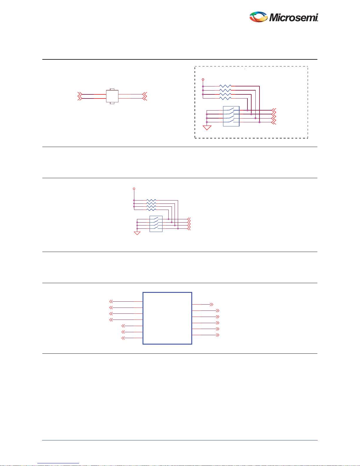
VAREF Connections . . . . . . . . . . . . . . . . . . . . . . . . . . . . . . . . . . . . . . . . . . . . . . . . . . . . . . . . . . . . . . . . . . . . . . . 19
Current Sensing Circuit . . . . . . . . . . . . . . . . . . . . . . . . . . . . . . . . . . . . . . . . . . . . . . . . . . . . . . . . . . . . . . . . . . . . . 20
PWM Circuit . . . . . . . . . . . . . . . . . . . . . . . . . . . . . . . . . . . . . . . . . . . . . . . . . . . . . . . . . . . . . . . . . . . . . . . . . . . . . . 20
Push-Button System Reset . . . . . . . . . . . . . . . . . . . . . . . . . . . . . . . . . . . . . . . . . . . . . . . . . . . . . . . . . . . . . . . . . . 21
Push-Button, DIP Switches, and User LEDs . . . . . . . . . . . . . . . . . . . . . . . . . . . . . . . . . . . . . . . . . . . . . . . . . . . . . 22
One-Bit DAC (OBD) Circuit . . . . . . . . . . . . . . . . . . . . . . . . . . . . . . . . . . . . . . . . . . . . . . . . . . . . . . . . . . . . . . . . . . 24
OLED Display . . . . . . . . . . . . . . . . . . . . . . . . . . . . . . . . . . . . . . . . . . . . . . . . . . . . . . . . . . . . . . . . . . . . . . . . . . . . 25
SPI Flash . . . . . . . . . . . . . . . . . . . . . . . . . . . . . . . . . . . . . . . . . . . . . . . . . . . . . . . . . . . . . . . . . . . . . . . . . . . . . . . . 28
SPI DAC . . . . . . . . . . . . . . . . . . . . . . . . . . . . . . . . . . . . . . . . . . . . . . . . . . . . . . . . . . . . . . . . . . . . . . . . . . . . . . . . . 29
2
C EEPROM . . . . . . . . . . . . . . . . . . . . . . . . . . . . . . . . . . . . . . . . . . . . . . . . . . . . . . . . . . . . . . . . . . . . . . . . . . . . . 30
I
Clock Oscillator . . . . . . . . . . . . . . . . . . . . . . . . . . . . . . . . . . . . . . . . . . . . . . . . . . . . . . . . . . . . . . . . . . . . . . . . . . . 32
USB-to-UART Interface . . . . . . . . . . . . . . . . . . . . . . . . . . . . . . . . . . . . . . . . . . . . . . . . . . . . . . . . . . . . . . . . . . . . . 33
RS485 Interface . . . . . . . . . . . . . . . . . . . . . . . . . . . . . . . . . . . . . . . . . . . . . . . . . . . . . . . . . . . . . . . . . . . . . . . . . . . 34
Ethernet Interface . . . . . . . . . . . . . . . . . . . . . . . . . . . . . . . . . . . . . . . . . . . . . . . . . . . . . . . . . . . . . . . . . . . . . . . . . 35
Memory Section Overview . . . . . . . . . . . . . . . . . . . . . . . . . . . . . . . . . . . . . . . . . . . . . . . . . . . . . . . . . . . . . . . . . . . 37
Using EMC I/Os as User I/Os . . . . . . . . . . . . . . . . . . . . . . . . . . . . . . . . . . . . . . . . . . . . . . . . . . . . . . . . . . . . . . . . 45
Controller Area Network (CAN) Interface . . . . . . . . . . . . . . . . . . . . . . . . . . . . . . . . . . . . . . . . . . . . . . . . . . . . . . . . 45
Ethernet for Control Automation Technology (EtherCAT) Interfa ce . . . . . . . . . . . . . . . . . . . . . . . . . . . . . . . . . . . . 46
Low Cost Programming Stick (LCPS) Header . . . . . . . . . . . . . . . . . . . . . . . . . . . . . . . . . . . . . . . . . . . . . . . . . . . . 47
RealView Header . . . . . . . . . . . . . . . . . . . . . . . . . . . . . . . . . . . . . . . . . . . . . . . . . . . . . . . . . . . . . . . . . . . . . . . . . . 48
Direct-C Programming Interface . . . . . . . . . . . . . . . . . . . . . . . . . . . . . . . . . . . . . . . . . . . . . . . . . . . . . . . . . . . . . . 49
FlashPro4 Programming Header . . . . . . . . . . . . . . . . . . . . . . . . . . . . . . . . . . . . . . . . . . . . . . . . . . . . . . . . . . . . . . 50
A2F500 Digital I/O Expansion Header . . . . . . . . . . . . . . . . . . . . . . . . . . . . . . . . . . . . . . . . . . . . . . . . . . . . . . . . . . 54
Mixed Signal Header . . . . . . . . . . . . . . . . . . . . . . . . . . . . . . . . . . . . . . . . . . . . . . . . . . . . . . . . . . . . . . . . . . . . . . . 56
4 Pin List . . . . . . . . . . . . . . . . . . . . . . . . . . . . . . . . . . . . . . . . . . . . . . . . . . . . . . . . . . . . . . . . . . . . . . . . . 61
Pin List for A2F500M3G-FGG484ES Devices . . . . . . . . . . . . . . . . . . . . . . . . . . . . . . . . . . . . . . . . . . . . . . . . . . . . 61
5 Board Stackup . . . . . . . . . . . . . . . . . . . . . . . . . . . . . . . . . . . . . . . . . . . . . . . . . . . . . . . . . . . . . . . . . . . 75
Revision 7 2
Page 3

Table of Contents
A2F500-DEV-KIT-2 Board Stack-Up . . . . . . . . . . . . . . . . . . . . . . . . . . . . . . . . . . . . . . . . . . . . . . . . . . . . . . . . . . . 75
6 Manufacturing Test. . . . . . . . . . . . . . . . . . . . . . . . . . . . . . . . . . . . . . . . . . . . . . . . . . . . . . . . . . . . . . . . 79
A2F500-DEV-KIT-2 Board Testing Procedures . . . . . . . . . . . . . . . . . . . . . . . . . . . . . . . . . . . . . . . . . . . . . . . . . . . 79
Jumper Settings for the Board Test . . . . . . . . . . . . . . . . . . . . . . . . . . . . . . . . . . . . . . . . . . . . . . . . . . . . . . . . . . . . 79
Installing the A2F500-DEV-KIT-2 Board USB Serial Driver . . . . . . . . . . . . . . . . . . . . . . . . . . . . . . . . . . . . . . . . . . 80
Hooking up the Board and Programming Stick . . . . . . . . . . . . . . . . . . . . . . . . . . . . . . . . . . . . . . . . . . . . . . . . . . . 80
Programming the A2F500-DEV-KIT-2 Board (SmartFusion cSoC Device) . . . . . . . . . . . . . . . . . . . . . . . . . . . . . . 82
Setting Up the Test Terminal . . . . . . . . . . . . . . . . . . . . . . . . . . . . . . . . . . . . . . . . . . . . . . . . . . . . . . . . . . . . . . . . . 85
Running the A2F500-DEV-KIT-2 Board Test . . . . . . . . . . . . . . . . . . . . . . . . . . . . . . . . . . . . . . . . . . . . . . . . . . . . . 89
A2F500-DEV-KIT-2 Board Failures . . . . . . . . . . . . . . . . . . . . . . . . . . . . . . . . . . . . . . . . . . . . . . . . . . . . . . . . . . . 112
A List of Changes . . . . . . . . . . . . . . . . . . . . . . . . . . . . . . . . . . . . . . . . . . . . . . . . . . . . . . . . . . . . . . . . . 113
B Product Support . . . . . . . . . . . . . . . . . . . . . . . . . . . . . . . . . . . . . . . . . . . . . . . . . . . . . . . . . . . . . . . . . 115
Customer Service . . . . . . . . . . . . . . . . . . . . . . . . . . . . . . . . . . . . . . . . . . . . . . . . . . . . . . . . . . . . . . . . . . . . . . . . 115
Customer Technical Support Center . . . . . . . . . . . . . . . . . . . . . . . . . . . . . . . . . . . . . . . . . . . . . . . . . . . . . . . . . . 115
Technical Support . . . . . . . . . . . . . . . . . . . . . . . . . . . . . . . . . . . . . . . . . . . . . . . . . . . . . . . . . . . . . . . . . . . . . . . . 115
Website . . . . . . . . . . . . . . . . . . . . . . . . . . . . . . . . . . . . . . . . . . . . . . . . . . . . . . . . . . . . . . . . . . . . . . . . . . . . . . . . 115
Contacting the Customer Technical Support Center . . . . . . . . . . . . . . . . . . . . . . . . . . . . . . . . . . . . . . . . . . . . . . 115
ITAR Technical Support . . . . . . . . . . . . . . . . . . . . . . . . . . . . . . . . . . . . . . . . . . . . . . . . . . . . . . . . . . . . . . . . . . . . 116
Index . . . . . . . . . . . . . . . . . . . . . . . . . . . . . . . . . . . . . . . . . . . . . . . . . . . . . . . . . . . . . . . . . . . . . . . . . 117
3 Revision 7
Page 4

Page 5
Introduction
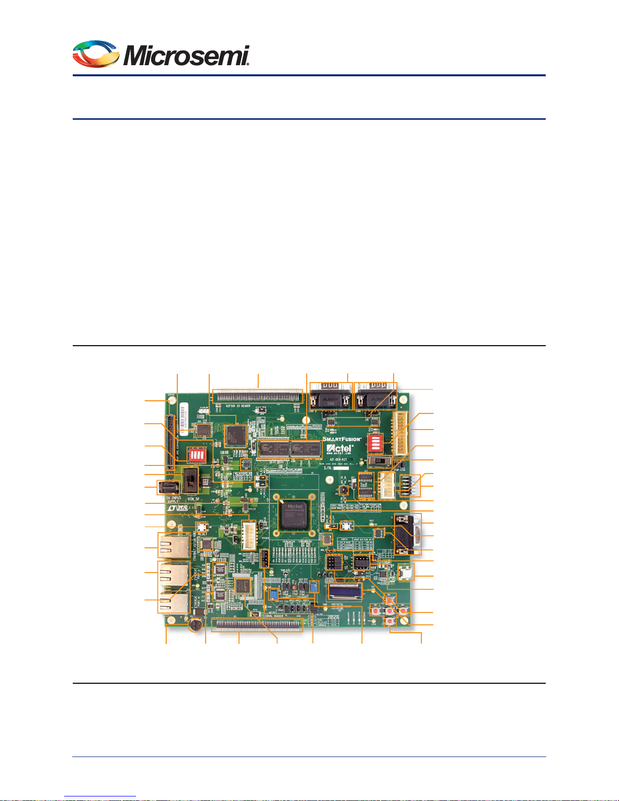
DirectC Header
Board Reset Switch
Power Jack
Memory Device
Configuration Headers
AGLP DIP Switch
AGLP125V5-
CSG289
IGLOO PLUS Header
10/100 Ethernet PHY
RJ45 Connector for
10/100 Ethernet
AGLP Header
DACOUT/
ADC Headers
RJ45 Connectors for
EtherCAT Ports
SmartFusion Device
DB9 Connector
for CAN0
SRAM
(3.3 V)
CAN
Transceivers
DB9 Connector
for CAN1
A2F500
Connector
PSRAM
(1.8 V)
LCPS Connector
FlashPro Header
DIP Switch
JTAG_SEL Switch
JTAG Chain Configuration Header
1.5 V Header
PUB Switch
RS485 Transceiver
DB9 Connector for RS485 (UART1)
50 MHz Oscillator
SPI Headers
I
2
C Headers
USB Connector for UART0
OLED
Push-Button
Switches
RealView
®
Header
JTAG MUX
EtherCAT
PHYs
DAC0 and DAC1
Callibration POTs for
±15 V Bipolar Outputs
POT for
Current Monitor
Mixed-Signal
Header
EtherCAT
ASIC
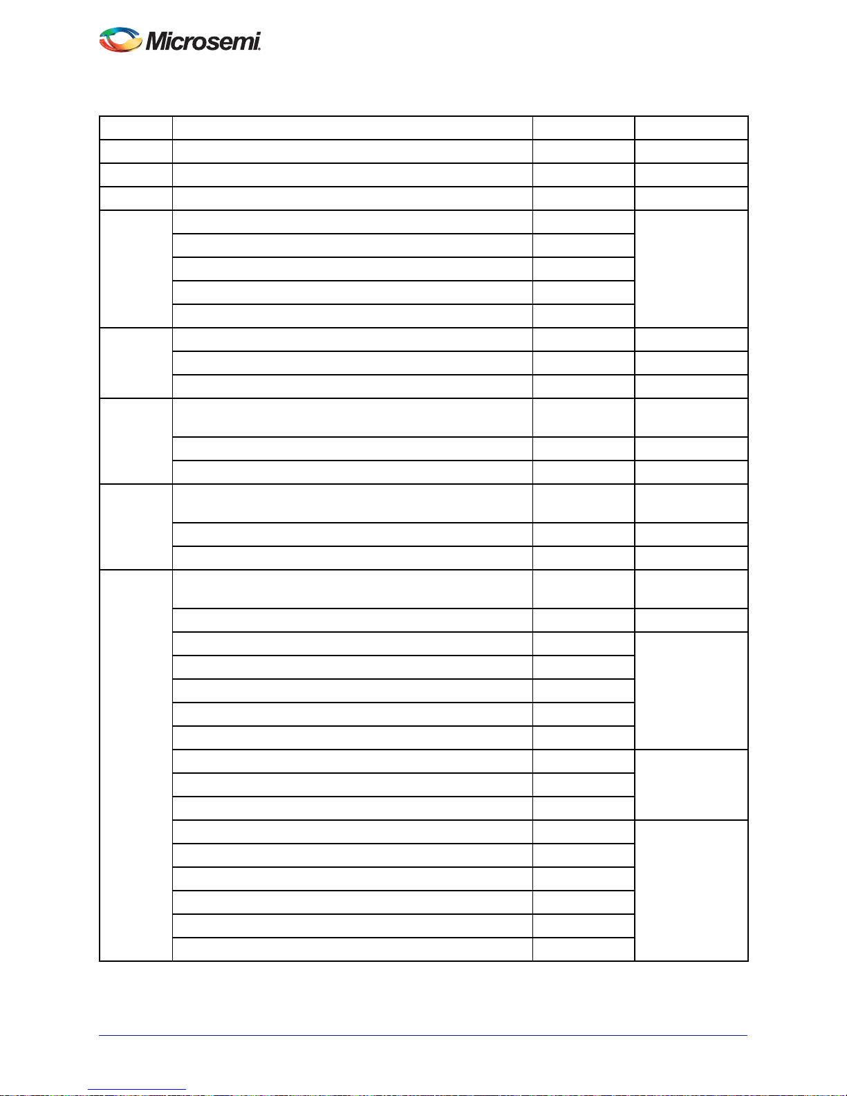
The RoHS-compliant SmartFusion® Development Kit (A2F500-DEV-KIT -2) enables designers to develop
applications that involve one or more of the following:
• Microcontroller applications
• Real-time operating system (RTOS)/OS development
• Embedded ARM
• Motor control
• System management
• Power sequencing, trimming, and management
• Touch screen display control
• Audio processing
•FieldBus
•EtherCAT
• Industrial network
The board also provides a standard 100-pin mixed signal header for interfacing to the analog pins. This
provides access for plugging in a daughter board with a mixed signal interface.
®
Cortex™-M3 processor based systems
®
demonstrator
®
Figure 1 • A2F500-DEV-KIT-2
Revision 7 5
Page 6
Introduction
Kit Contents
Table 1 lists the contents of the SmartFusion Development Kit.
Table 1 • Kit Contents – A2F500-DEV-KIT-2
Quantity Description
1 SmartFusion Development Board with SmartFusion A2F500M3G-FGG484ES device
1 Low-cost programming stick (LCPS) or FlashPro 4 programmer
1 5 V power supply with international adapters
2 USB 2.0 A to mini-B cable
1 Quickstart card
SmartFusion Development Kit Web Resources
The SmartFusion Development Kit web resources are available on the Microsemi website:
www.microsemi.com/soc/products/hardware/devkits_boards/smartfusion_dev.aspx#rsc.
Board Description
The SmartFusion Development Kit Board is designed to pro vide a development platform for users to
evaluate all the features of the world’s only customizable system-on-chip (cSoC) with a hard ARM
Cortex-M3 processor powered microcontroller subsystem (MSS) along with programmable analog.
The board supports a SmartFusion cSoC device in an FG484 package. To enable the MSS, analog, and
evaluation of features, the board includes the following:
• Ethernet, EtherCAT, and USB-to-UART interface for communication with Ethernet and UART
peripherals of the SmartFusion MSS
• Static random access memory (SRAM), parallel flash, SPI flash, and electrically erasable
programmable read-only memory (EEPROM) that interface with EMC, SPI, and I2C peripherals of
the SmartFusion MSS
• Digital-to-analog converter (DAC) that interfaces either to SPI port 0 or SPI port 1 of the
SmartFusion MSS
• Organic light-emitting diode (OLED) that interfaces with either SPI or I
SmartFusion MSS
•I2C interface and temperature monitoring
• Mixed signal header for daughter card interfacing
• RealView ICE Simulation Unit (RVI) header for application programming and debug from either
®
Keil
ULINK® or IAR J-link
The board includes a FlashPro4 programming header to enable programming and debugging from
Microsemi design tools FlashPoint and SoftConsole.
®
2
C peripherals of the
6 Revision 7
Page 7

SmartFusion Development Kit
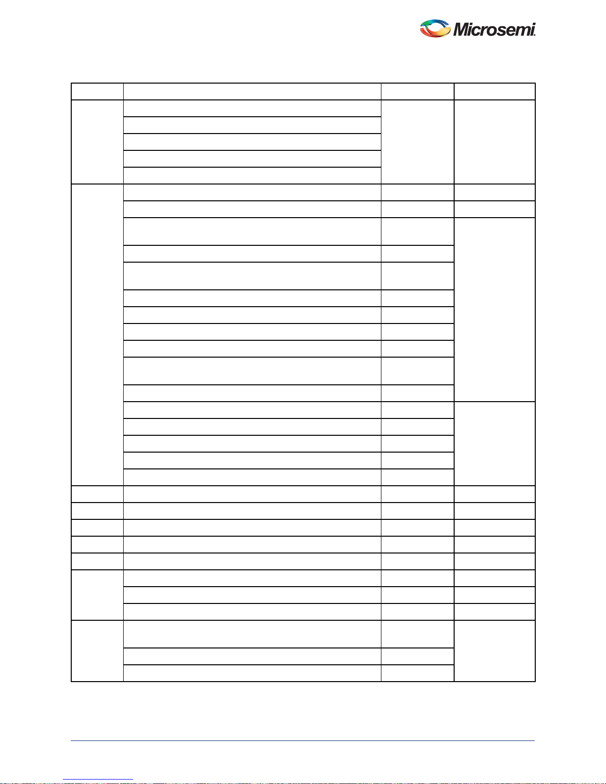
Table 2 describes SmartFusion Development Kit Board Components.
.
Table 2 • SmartFusion Development Kit Board Components
Name Description
A2F500M3G-FGG484ES Microsemi SmartFusion cSoC with hard ARM Cortex-M3 processor
CURRENT SENSING Current monitoring using thumbwheel POT (RV1)
PWM CIRCUIT Pulse Width Modulation Resistor Capacitor (PWMRC) circuit
OBD Three one-bit DACs used in comparator
OLED DISPLAY Organic 96×16 pixel
white OLED PMO18701 with option to interface to I
2
C port 0 or SPI
port 0 of the SmartFusion MSS
I2C EEPROM 512 Kbit I
2
C EEPROM ST M24512-WMN6TP connected to I2C port 1 of the SmartFusion
MSS
SPI FLASH 8 MByte SPI flash Atmel AT25DF641-MWH-T connected to SPI port 1 of the SmartFusion
MSS
SPI DAC 12-bit SPI DAC AD5320 with option to interface either to SPI port 0 or SPI port 1 of the
SmartFusion MSS
OSC-50 50 MHz clock oscillator
OSC-20 20 MHz/20 PPM clock oscillator
OSC-32 32.768 KHz low power oscillator
USB/UART USB-to-UART adapter chip CP2102 and connector interfacing with UART Port 0 of the
SmartFusion MSS
RS485 RS485 with DB9 female connector interfacing with MAX3240CSA, connected to UART
port 1 of the SmartFusion MSS
ETHERNET RJ45 connector (Ethernet jack with magnetics) interfacing with National Semiconductor
10/100 PHY chip DP83848C in RMII mode, interfacing with Ethernet port of the
SmartFusion MSS (on-chip MAC and external PHY)
®
AGLP125-CS289 IGLOO
PLUS FPGA implementing level converter between 3.3 V and 1.8 V to connect
1.8 V PSRAM/flash with external memory controller (EMC, which has native voltage level
of 3.3 V) of the SmartFusion MSS
EXPANSION When external memory controller (EMC) is not used, the I/Os are available as
3.3 V GPIOs.
Asynchronous SRAM Two 16-Mbit SRAM Cypress CY7C1061DV33-10ZSXI connected to each region of the
EMC interface of the SmartFusion MSS
FLASH Two 64-Mbit parallel flash memory Numonyx JS28F640J3D-75 connected to each region
of the EMC interface of the SmartFusion MSS
LG_PSRAM 128-Mbit, 1.8 V asynchronous PSRAM Micron MT45W8MW16BGX connected to the EMC
interface of the SmartFusion MSS. This provides the option of bigger memory as an
alternative to the SRAM for memory intensive applications.
LG_FLASH 128-Mbit, 1.8 V, parallel flash memory Numonyx JS28F128P30T85 873824 connected to
the EMC interface of the SmartFusion MSS. This provides the option of bigger memory as
an alternative to the flash for memory intensive applications.
CAN_IF Two CAN interfaces with DB9 female connector interfacing with MAXIMMAX3051 CAN
transceiver connected to four GPIOs of the SmartFusion MSS
Revision 7 7
Page 8
Introduction
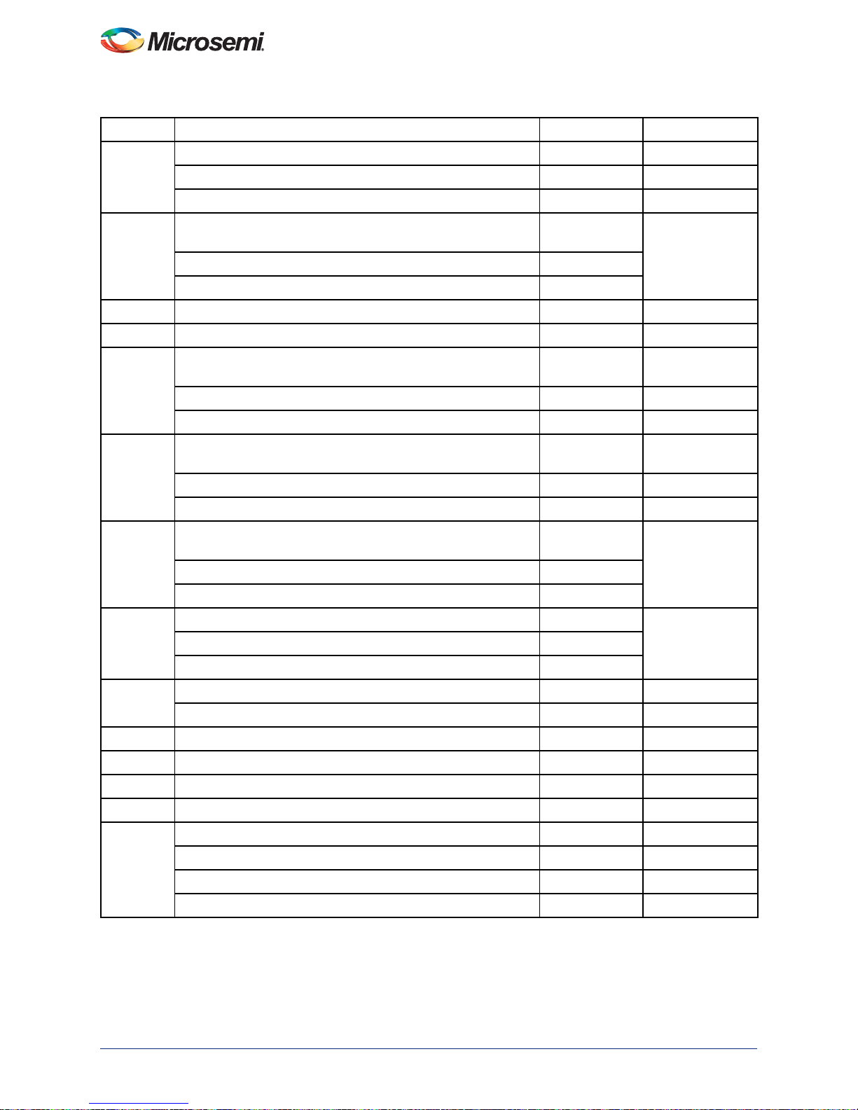
Table 2 • SmartFusion Development Kit Board Components (continued)
Name Description
ETHERCAT_IF Two RJ45 connectors (Ethernet jack with magnetics) for EtherCAT ports interfacing with
Beckhoff ET1 100 and Micrel KS8721BL and connecting to the SmartFusion cSoC via soft
SPI implemented in the fabric using six general purpose I/Os
RVI HEADER RVI header for application programming an d debug from Keil ULINK or IAR J-Link
FP4 Programming
HEADER
Flashpro4 programming header for FPGA and cSoC programming and debugging with
Microsemi tools
PROG HDR Direct-C programming header
TEMP DIODE Temperature diode
BATT BACKUP Battery backup circuit
DIPSWITCH Two 4-switch DIP switch packs for GPIO
LEDS Four active Low LEDs that can be connected to any user I/O for debug to power-on the
board
PUSH-BUTTON RESET Push-button system reset for SmartFusion System
MIXED_CONN100 To power-on the board mixed signal header
PUSH-BUTTON
Six push-button switches for test and navigation and PUB
SWITCHES
MIXED_CONN100 Mixed signal header
A2F500_CONN100 Microsemi SmartFusion A2F500M3F-FG484ES additional I/O connector
8 Revision 7
Page 9
1 – Installation and Settings
Software Installation
Download and install the latest release of Microsemi Libero® Integrated Design Environment (IDE), v9.0
or later, from the Microsemi website and register for your free Gold license. For instructions on how to
install Libero IDE and SoftConsole, refer to the Libero IDE Installation and Licensing Guide, available on
the Microsemi website. Refer to the Installing IP Cores and Drivers User’s Guide for download and
installation of Microsemi DirectCores, SGCores, and Driver firmware cores that must be localized on the
personal computer where Microsemi's Libero IDE is installed when designing with Microsemi FPGAs and
cSoCs. Microsemi has partnered with key industry leaders in the microcontroller space to provide the
robust SmartFusion ecosystem. Microsemi SmartFusion is supported by the latest release of IAR
Systems, the IAR Embedded Workbench for ARM. Refer to Designing SmartFusion with IAR Systems
document for more information. The Microsemi SmartFusion cSoC is also supported by the latest
release of Keil, the MDK-ARM Microcontroller Development Kit. Refer to the Designing SmartFusion with
Keil document for more information.
Hardware Installation
The FlashPro4 (FP4) programmer plugs directly into the A2F500-DEV-KIT-2 board. This allows
programming A2F500 and AGLP125 devices in chain mode or individually with appropriate jumper
settings (JP5).
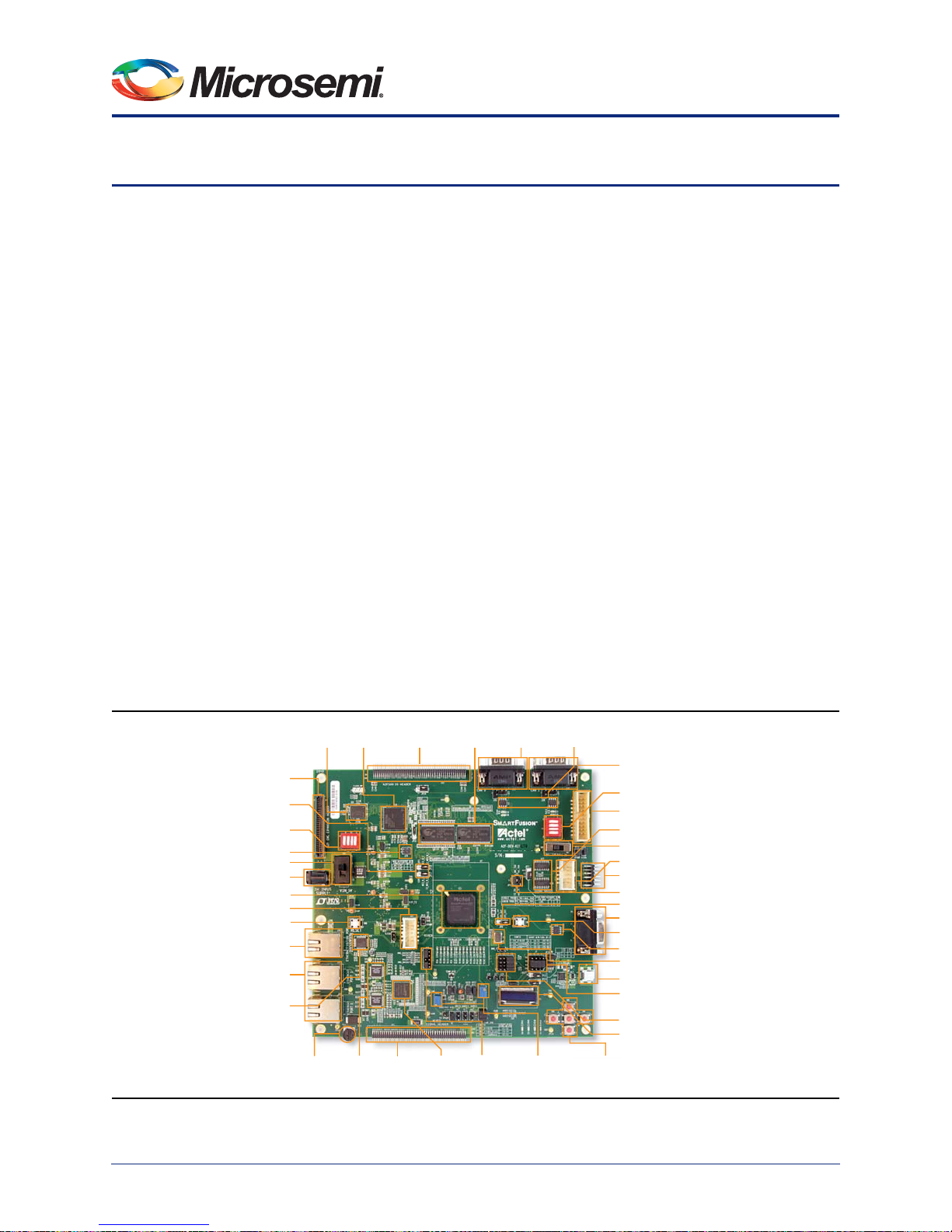
Jumpers, Switches, LEDs and DIP Switch Settings
The recommended default jumpers, switches, LEDs, and dual in-line package (DIP) switch settings are
shown in Figure 1-1 and defined in Table 1-1 on page 10 through Table 1-4 on page 13. Connect the
jumpers with the default settings to enable the pre-programmed demonstration design to function
correctly.
IGLOO PLUS Header
Memory Device
Configuration Headers
AGLP DIP Switch
AGLP Header
Power Jack
SmartFusion Device
DirectC Header
Board Reset Switch
RJ45 Connector for
10/100 Ethernet
RJ45 Connectors for
EtherCAT Ports
10/100 Ethernet PHY
PSRAM
(1.8 V)
POT for
Current Monitor
AGLP125V5-
CSG289
EtherCAT
PHYs
A2F500
Connector
Mixed-Signal
Header
EtherCAT
ASIC
SRAM
(3.3 V)
DACOUT/
ADC Headers
DB9 Connector
for CAN0
Callibration POTs for
±15 V Bipolar Outputs
Transceivers
DAC0 and DAC1
CAN
DB9 Connector
for CAN1
DIP Switch
®
RealView
JTAG MUX
JTAG_SEL Switch
FlashPro Header
LCPS Connector
JTAG Chain Configuration Header
1.5 V Header
DB9 Connector for RS485 (UART1)
PUB Switch
RS485 Transceiver
50 MHz Oscillator
USB Connector for UART0
2
C Headers
I
SPI Headers
OLED
Push-Button
Switches
Header
Figure 1-1 • Jumper Locations
Revision 7 9
Page 10
Installation and Settings
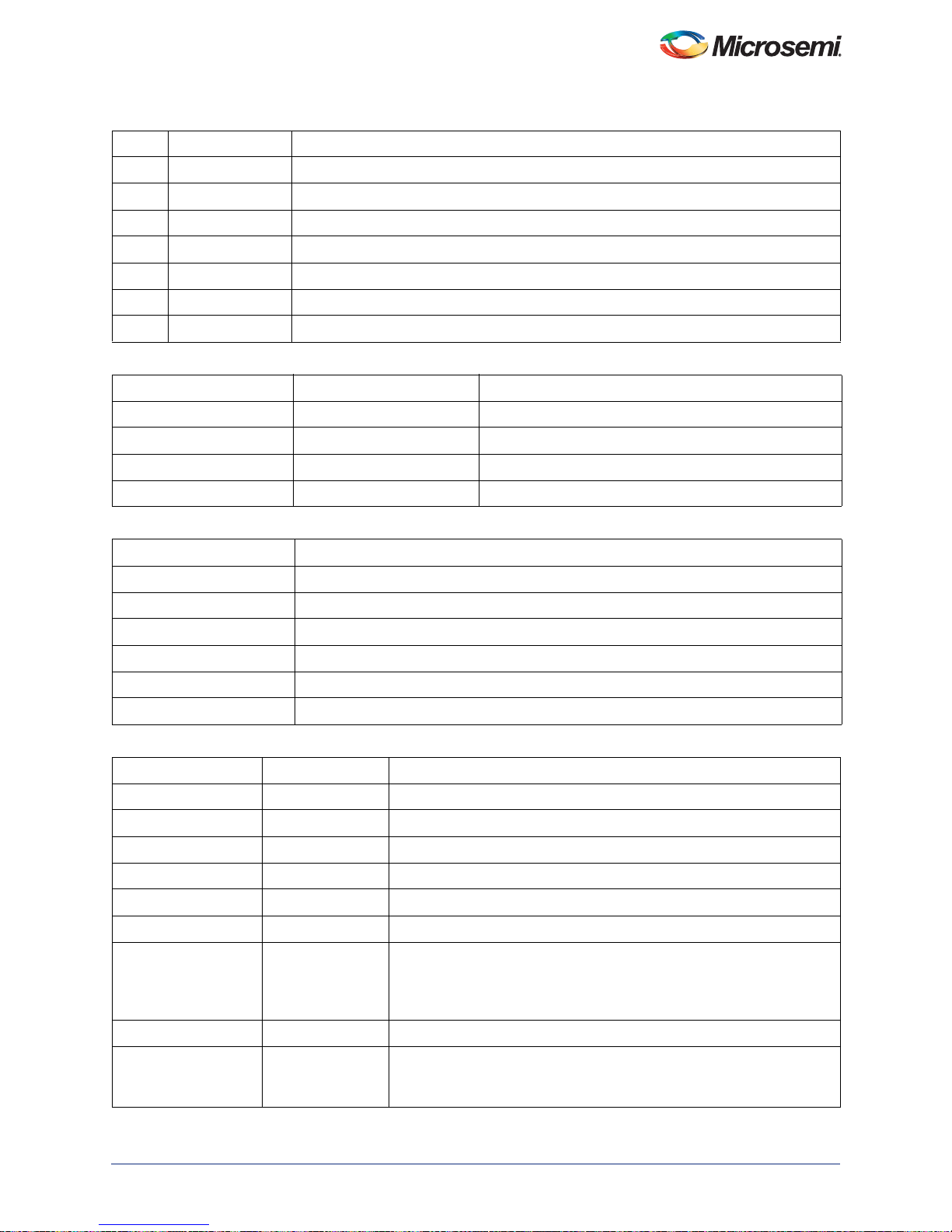
Table 1-1 • Jumper Settings
Jumper Function Default Setting Notes
JP1 Jumper to select first 3.3 V power supply for board 1–2 Closed
JP2 Jumper to select second 3.3 V power supply for board 1–2 Closed
JP3 Jumper for SPI DAC output VOUT Open
JP4 Jumper settings to use comparator Pins 2, 6,10 are
Pin 3–4 = DACOUT0 to ADC0 Open
connected to
AGND
Pin 7–8 = DACOUT1 to ADC1 Open
Pin 1–3 = DACOUT0 to OBD_DACOUT0 Closed
Pin 7–9 = DACOUT1 to OBD_DACOUT1 Closed
JP5 Jumper for JTAG device option (A2F500 and AGLP125)
Pin 1–3 = A2F500 in chain Open
Pin 1–2 and Pin 4-3 = A2F500 and AGLP125 daisy chained Closed
JP6 Jumper to select either 1.5 V external regulator or SmartFusion
cSoC device 1.5 V internal regulator
Pin 1–2 = 1.5 V internal Open
Pin 3–2 = 1.5 V external Closed
JP7 Jumper to select between RVI header or LCPS header for
application debug
Pin 1–2 = LCPS for SoftConsole Closed
Pin 2–3 = RVI for Keil U-link/ IAR J-link Open
2
J7 Jumper/Header for SPI_0, I
C, EEPROM, OLED, and I2C
loopback
I2C0 to OLED
Pin 2–3 = I2C_0_SCL to OLED_SCL Closed Configuration 1:
Pin 14–15 = I2C_0_SDA to OLED_SDA_IN Closed
I2C0 -> OLED and
I2C1 -> EEPROM
I2C1 to EEPROM
Pin 6–7 = I2C_1_SCL to EEPROM_SCL Closed
Pin 10–11 = I2C_1_SDA to EEPROM_SDA Closed
I2C0 and I2C1 Loopback Configuration 2:
Pin 2–6 = I2C_0_SCL to I2C_1_SCL Open
I2C0 <-> I2C1
(Loop Back)
Pin 10–14 = I2C_1_SDA to I2C_0_SDA Open
SPI to OLED Configuration 3:
Pin 3–4 = SPI_SCK to OLED_SCL Open
SPI -> OLED and
I2C1 -> EEPROM
Pin 15–16 = SPI_SDA to OLED_SDA Open
I2C1 to EEPROM
Pin 6–7 = I2C_1_SCL to EEPROM_SCL Closed
Pin 10–11 = I2C_1_SDA to EEPROM_SDA Closed
10 Revision 7
Page 11
SmartFusion Development Kit
Table 1-1 • Jumper Settings (continued)
Jumper Function Default Setting Notes
J20 From AGLP125 CS289 Closed These pins are
Pin 1=AGLP_3.3V_SIG1
Pin 2=AGLP_3.3V_SIG2
brought out for
future and testing
purpose.
Pin 3=AGLP_3.3V_SIG3
Pin 4=AGLP_3.3V_SIG4
JP8 Jumper/Header for SPI, OLED, SPI flash, and loopback
SPI_0 to OLED
Pin 1–2 = SPI_0_OUT to OLED_SDA_IN (Need shunt pin 15–
Open Configuration 1:
16 jumper on J7)
Pin 5–6 = SDI_0_IN to OLED_SDA_OUT Open
Pin 9–10 = SCLK_0_OUT to OLED_SCL (Need shunt pin 3–4
Open
jumper on J7)
Pin 13–14 = SS_0_OUT to OLED_CS# Open
SPI_1 to SPI flash
Pin 3–4 = SDI_1_IN to SPI_1_SO (SO output of SPI flash) Closed
Pin 7–8 = SDO_1_OUT to SPI_1_SI (SI input of SPI flash) Closed
Pin 11–12 = SCLK_1_OUT to SPI_1_SCK (SCK input of SPI
Closed
flash)
Pin 15–16 = SS_1_OUT to SPI_CS_N (CS# input of SPI flash) Closed
SPI0 to SPI1 (loopback) Configuration 2:
Pin 2–3 = SDO_0_OUT to SDI_1_IN Open
Pin 6–7 = SDI_0_IN to SDO_1_OUT Open
Pin 10–11 = SCLK_0_OUT to SCLK_1_OUT Open
Pin 14–15 = SS_0_OUT to SS_1_OUT Open
JP11 Jumper to connect 3.3 V to VJTAG 1–2 Closed
JP12 Jumper to connect 3.3 V to VPUMP 1–2 Closed
JP13 VREF_OUT to OP_AMP (U44A & U51A) positive 1–2 Closed
JP14 OP_AMP (U44C) output to ABPS0 of FPGA fabric 1–2 Open
SPI_0 to OLED
and SPI_1 to SPI
flash
SPI0 and SPI1
loopback
JP15 OP_AMP (U44C) output to ABPS4 of FPGA fabric 1–2 Open
JP16 Jumper to control F*F of AGLP125 device
Pin 1–2 = F*F connected to 3.3 V (deasserted) Open
Pin 2–3 = F*F connected to GND (asserted) Closed
JP17 Jumper to select between 1.8 V and 3.3 V memory Interface
connected to region 0 of EMC
Pin 1–2 = 1.8 V interface Open
Pin 2–3 = 3.3 V interface Closed
To keep 3.3 V
devices tristated
Revision 7 11
Page 12
Installation and Settings
Table 1-1 • Jumper Settings (continued)
Jumper Function Default Setting Notes
JP18 Jumper to connect OLED_SDA_OUT and OLED_SDA_IN
2
Pin 1–2 = Closed for I
C configuration mode Closed
Pin 1–2 = Open for SPI mode
JP19 Jumper to select between 1.8 V and 3.3 V memory interface
connected to EMC
To keep 3.3 V
devices tristated
Pin 1–2 = 1.8 V interface Open
Pin 2–3 = 3.3 V interface Closed
JP20 Jumper to select positive 10 V power supply for board Closed
JP21 OP_AMP (U51C) output to ABPS1 of FPGA fabric 1–2 Open
JP22 Jumper to connect OLED_BS1 (MCU interface selection Input)
to 3.3 V or GND
2
Pin 1–2 = 3.3 V (needed for I
C mode) Open
Pin 2–3 = GND (needed for SPI mode) Closed
JP23 Jumper to connect OLED_BS2 (MCU interface selection input)
to 3.3 V or GND
Pin 1–2 = 3.3 V Closed
Pin 2–3 = GND (needed for both I2C & SPI modes) Open
JP24 Jumper to connect FLASH_VPEN of 64-Mbit parallel flash
connected to both regions of EMC
Identified as
FLASH
Pin 1–2 = FLASH_VPEN to 3.3 V (enabled) Closed
Pin 2–3 = FLASH_VPEN to GND (disabled) Open
JP25 Jumper to connect FLASH_WP# of 128-Mbit parallel flash Identified as
Pin 1–2 = FLASH_WP# to 1.8 V (disabled) Open
LG_FLASH
Pin 2–3 = FLASH_WP# to GND (enabled) Closed
JP26 Jumper to connect WE_N of EEPROM to 3.3 V
Pin 1–2 = 3.3 V (EEPROM write disabled) Closed
JP27 OP_AMP (U51C) output to ABPS5 of FPGA fabric
JP28 Jumper to select 1.8 V power supply for board 1–2 Closed
JP30 Jumper to connect VJTAG of PROG HDR to 3.3 V Open
JP31 Jumper to connect VPUMP of PROG HDR to 3.3 V Open
J32 VAREFOUT to ADC0, ADC1, ADC2 VAREF inputs
1–2 VAREFOUT to VAREF0 Closed
3–4 VAREFOUT to VAREF1 Closed
5–6 VAREFOUT to VAREF2 Closed
12 Revision 7
Page 13
SmartFusion Development Kit
Table 1-2 • SmartFusion Development Kit LEDs
LED SmartFusion Pin Comment
D1 B19 Test LED for user application
D2 B20 Test LED for user application
D3 C19 Test LED for user application
D4 H17 Test LED for user application
D5 N/A 5 V Power Supply Indicator LED. This LED is ON when board is powered on
D6 N/A SPEED LED: The LED is ON when device is in 100 Mbps and OFF when in 10 Mbps.
D8 N/A UART over USB link indicator LED
Table 1-3 • SmartFusion Development Board DIP Switches
DIP Switch (S1) SmartFusion Pin Comment
DIP1 H20 Test switch for user application
DIP2 C21 Test switch for user application
DIP3 D21 Test switch for user application
DIP4 F19 Test switch for user application
Table 1-4 • SmartFusion Development Kit Test Points
T est Point Comment
TP1, TP12 5 V power supply (measures 4.3 V due to diode drop)
TP2, TP5, TP6, TP7, TP8 Digital ground (GND)
TP3, TP4, TP13 Analog ground (AGND)
TP9 10 V rail for OLED
TP10 3.3 V supply for SmartFusion
TP11 3.3 V analog supply
Table 1-5 • SmartFusion Development Kit Push-Button Switches
Push-Button Switch SmartFusion Pin Comment
SW1 G19 Test and navigation switch
SW2 G20 Test and navigation switch
SW3 G21 Test and navigation switch
SW4 E1 Tes t and navigation switch
SW5 E14 Test and navigation switch
SW6 N/A Switch ON 5 V DC into SmartFusion cSoC device regulators
SW7 W7 Push-button switch for PUB. This negative active switch is connected to
the PUB pin, which is a digital input to the FPGA fabric. PUB is the
connection for the external momentary switch used to turn on the 1.5 V
voltage regulator.
SW8 R1 System reset for DUT
SW9 R16 (JTAGSEL) Switch to select A2F500 programming with FlashPro4 or Cortex-M3
processor debug. OFF position selects A2F500 programming and ON
position selects Cortex-M3 processor for application debug.
Revision 7 13
Page 14

Installation and Settings
Testing the Hardware
If the board is shipped directly from Microsemi, it contains a test program that determines whether the
board works properly. If while using the board you suspect that the board is damaged, you can rerun the
"Manufacturing Test" on page 79 to verify the key components of the board functionality.
14 Revision 7
Page 15

2 – Hardware Components
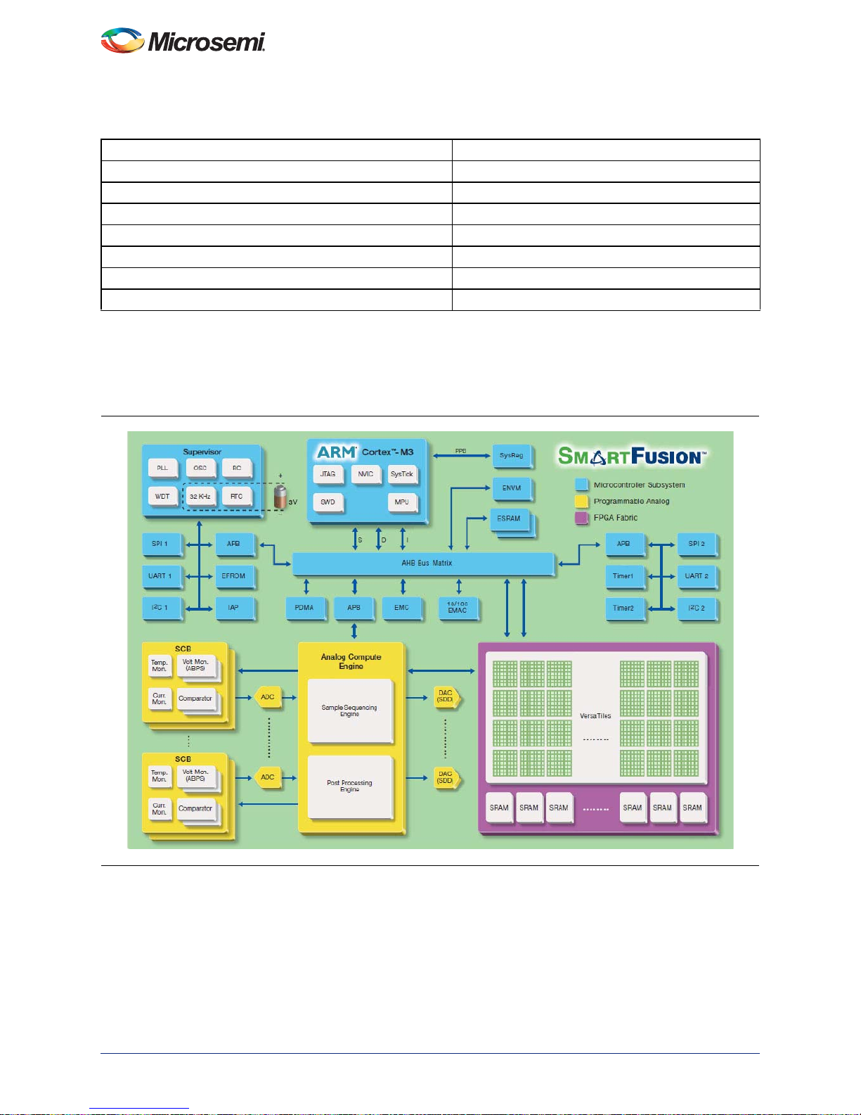
SmartFusion cSoC Description and Connections
The SmartFusion Development Kit Board is populated with a SmartFusion A2F500M3G-FGG484ES, the
world’s only cSoC with hard ARM Cortex-M3 processor. The key features of the SmartFusion cSoC are
listed below and in Table 2-1 on page 16.
The MSS consists of the following:
• 100 MHz 32-Bit ARM Cortex-M3 1.25 DMIPS/MHz throughput from zero wait state memory
• Internal memories
– Embedded flash memory (eNVM), 64 Kbytes to 512 Kbytes
– Embedded high-speed SRAM (eSRAM), 16 Kbytes to 64 Kbytes, implemented in two physical
blocks to enable simultaneous access from two different masters
• Multi-layer AHB communications matrix
– Provides up to 16 Gbps of on-chip memory bandwidth
• 10/100 Ethernet MAC with RMII interface
• Programmable external memory controller, which supports:
– Asynchronous memories
– NOR flash, SRAM, PSRAM
– Synchronous SRAMs
•Two I
• Two 16550 compatible UARTs
• Two SPI peripherals
• Two 32-bit timers
• 32-bit watchdog timer
• 8-Channel DMA controller
• Clock sources
• High-performance FPGA fabric
• Based on Microsemi's proven ProASIC
• Analog front-end (AFE)
• Up to three 12-Bit SAR ADCs
• One first-order ΣΔ DAC (sigma-delta) per ADC
• Up to five new high-performance analog signal conditioning blocks (SCB) per device
• Two high-speed comparators
• Analog compute engine (ACE)
2
C peripherals
– 1.5 MHz to 20 MHz main oscillator
– Battery-backed 32 KHz low-power oscillator with real-time counter (RTC)
– 100 MHz embedded RC oscillator 1% accurate
– Embedded PLL with 4 ou tput phases
®
3 FPGA fabric
– Offloads CPU from analog initialization and processing of ADC, DAC, and SCBs
– Sample sequence engine for ADC and DAC parameter set-up
– Post-processing engine for functions such as low-pass filtering and linear transformation
Revision 7 15
Page 16
Hardware Components
Table 2-1 • A2F500 I/Os
Device Package
A2F500 FG484
Direct analog input 12
Total analog input 32
Total analog output 3
MSS I/Os
FPGA I/Os 128
Total I/Os 204
Notes:
1. 16 MSS I/Os are multiplexed and can be used as FPGA I/Os, if no t needed for the MSS. These I/Os support
2. 9 MSS I/Os are primarily for 10/00 Ethernet MAC and are also multiplexed and can be used as FPGA I/Os if
1, 2
Schmitt triggers and support only LVTTL and LVCMOS (1.5 / 1.8 / 2.5, and 3.3 V) standards.
Ethernet MAC is not used in a design. These I/Os support Schmitt triggers and support only LVTTL and LVCMOS
(1.5 / 1.8 / 2.5, and 3.3 V) standards.
41
Figure 2-1 • SmartFusion Block Diagram
I/O Pin Connections
The pin list is provided in the "Pin List" section on page 61.
16 Revision 7
Page 17

SmartFusion Development Kit
SmartFusion cSoC Hard ARM Cortex-M3 Processor
The SmartFusion cSoC comes with a hard Cortex-M3 advanced processor-based MSS. The ARM
Cortex-M3 microcontroller is a low power processor that features low gate count, low predictable
interrupt latency, and low-cost debug. It is intended for deeply embedded applications that require fast
interrupt response features. SmartFusion cSoCs use the R1P1 version of the Cortex- M3 processor core.
Some of the important subsystems are listed below:
• Memory protection unit (MPU)
• Single-cycle multiplication and hardware divide
• JTAG debug (4 wire), Serial Wire Debug (SWD – 2 wire) and serial wire viewer (SWV) interfaces
The development board is populated with components to enable development using the MSS. These
components include SRAM, PSRAM, flash, SPI flash, I2C, EEPROM, OLED, SPI DAC, communication
interfaces such as Ethernet, and USB-to-UART.
Revision 7 17
Page 18

Hardware Components
Power Sources
This board is powered through an external 5 V power supply brick.
SmartFusion Power Sources
Seven voltage rails (10 V, 5 V, 3.3 V, 1.8 V, 1.5 V, and ± 15 V) are provided on the board:
• A single regulator, Linear LT3684EMSE (3.3 V, 2 A), supplies both analog and digital 3.3 V going
to the SmartFusion cSoC device. Sufficient isolation is provided through low-pass filter and layout
to prevent noise from the digital domain to propagate to the analog domain.
• Linear LT3684EMSE (1.8 V, 2 A), supplies 1.8 V rails.
• Linear LT3684EMSE (1.5 V, 2 A), supplies 1.5 V rails.
• Linear LT1615 step-up converter supplies 10 V, 100 mA typical, for driving OLED.
• A single regulator, Linear L T1615, supplies both the +15 V and –15 V with 4 mA rating required by
the DAC comparators.
18 Revision 7
Page 19

3 – Components Description and Operation
VAREF_OUT
VAREF_1
VAREF_OUT
VAREF_OUT
VAREF_OUT
VAREF_0
VAREF_1
VAREF2
VAREF2
VAREF_0
AGND
AGND
AGND
AGND
AGND
C63
10uF
C63
10uF
12
J5
HEADER 1x2
J5
HEADER 1x2
2
4
6
1
3
5
J32
HEADER 3X2
J32
HEADER 3X2
C62
10uF
C62
10uF
1
J2
HEADER 1
J2
HEADER 1
12
J6
HEADER 1x2
J6
HEADER 1x2
C61
10uF
C61
10uF
C79
10uF
C79
10uF
12
J8
HEADER 1x2
J8
HEADER 1x2
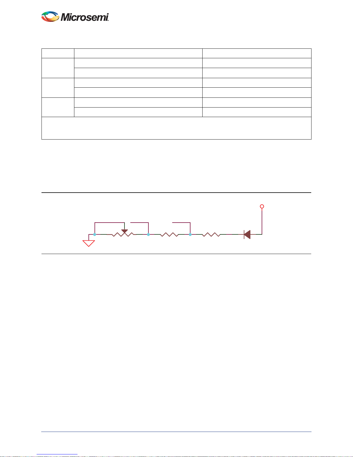
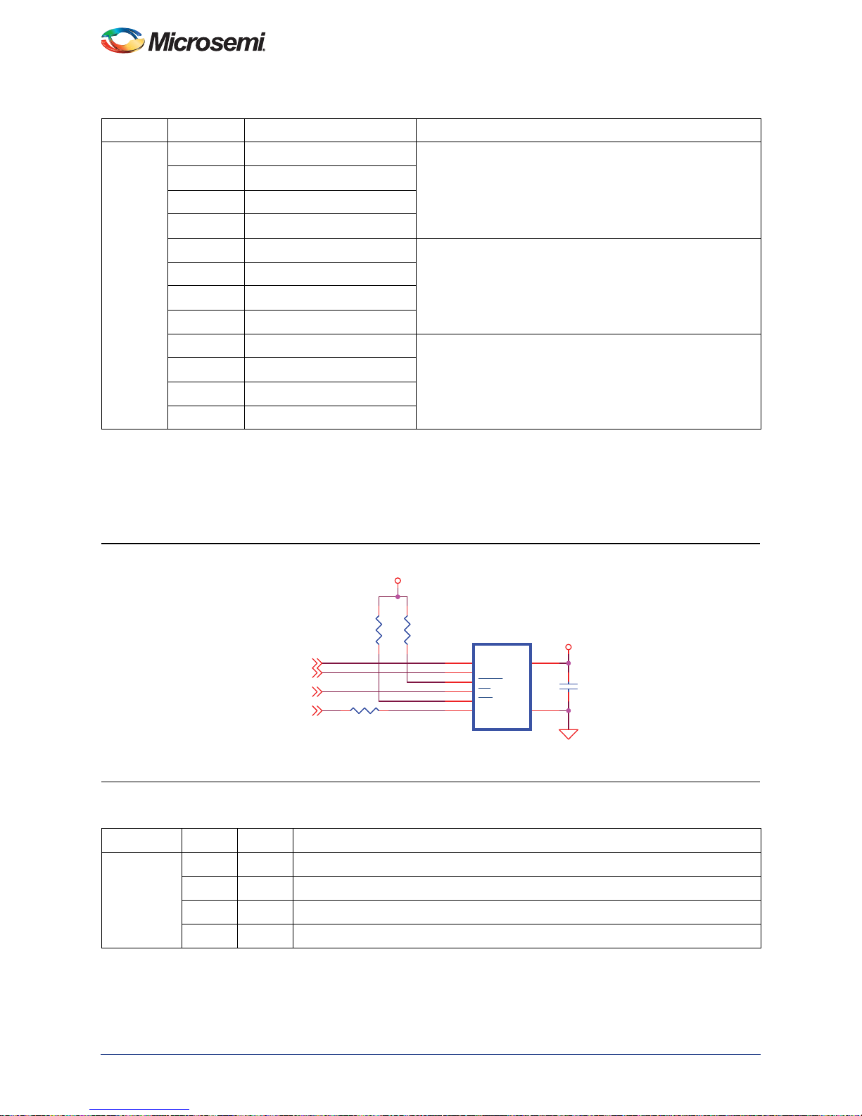
VAREF Connections
The SmartFusion cSoC has one external VAREF input pin for each of the ADCs. The internal VAREF is
brought out as an output, available as VAREFOUT output pin. There are multiple options available to
drive the VAREF0 and VAREF1 from either external VAREF or the internal VAREF through VAREFOUT
output of the FPGA fabric.
Figure 3-1 • VAREF Jumper Selections
Table 3-1 • Use as Internal VAREF
Jumper Function
J32 1–2 VAREFOUT to VAREF0
Notes:
VAREF0 corresponds to ADC[3:0], CM[1:0], TM[1:0]
VAREF1 corresponds to ADC[7:4], CM[3:2], TM[3:2]
VAREF2 corresponds to ADC[11:8], CM4, TM4 (A2F500 only)
3–4 VAREFOUT to VAREF1
5–6 VAREFOUT to VAREF2
Revision 7 19
Page 20
Components Description and Operation
Table 3-2 • Using External VAREF
VAREF Jumper Settings Comment
VAREF0 J32: 1–2 Open
Connect external voltage across J8 pins 1–2 Do not place a jumper on J8
VAREF1 J32: 3–4 Open
Connect external voltage across J5 pins 1–2 Do not place a jumper on J5
VAREF2 J32: 5–6 Open
Connect external voltage across J6 pins 1–2 Do not place a jumper on J6
Note: You need an external VAREF to monitor voltages greater than 2.56 V on the DC/AC/AT channels. An internal
VREF is sufficient to monitor voltages less than 2.56 V on the ADC/AC/AT channels. All ABPS channels can
monitor voltages greater than 2.56 V using an internal VREF.
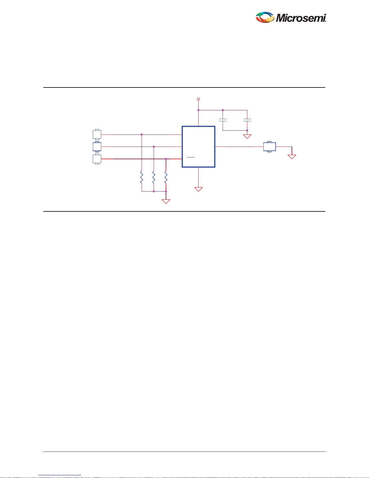
Current Sensing Circuit
For applications using the embedded current monitor, a current sensing circuit is provided on the
SmartFusion Development Kit board. The current monitoring is performed across AC0 and AT0 pins of
the SmartFusion cSoC device. The voltage across the potentiometer can be monitored via the AT0 pin.
The current sensing circuits is for the 3.3 V voltage rail as shown in Figure 3-2.
3
RV1
RV1
Figure 3-2 • Current Sensing
Note: The current monitoring circuit on the SmartFusion Development Kit board is connected to the
SmartFusion cSoC devices CM0 and TM0 inputs. CM0 can also be used to monitor the voltage
across the potentiometer. This input does not have a prescaler circu it. Because of the value chosen
for the potentiometer, the full-scale input is reached after turning the potentiometer about one
quarter of the maximum travel. Although this will not damage the SmartFusion cSoC device, you
may notice the potentiometer is very sensitive.
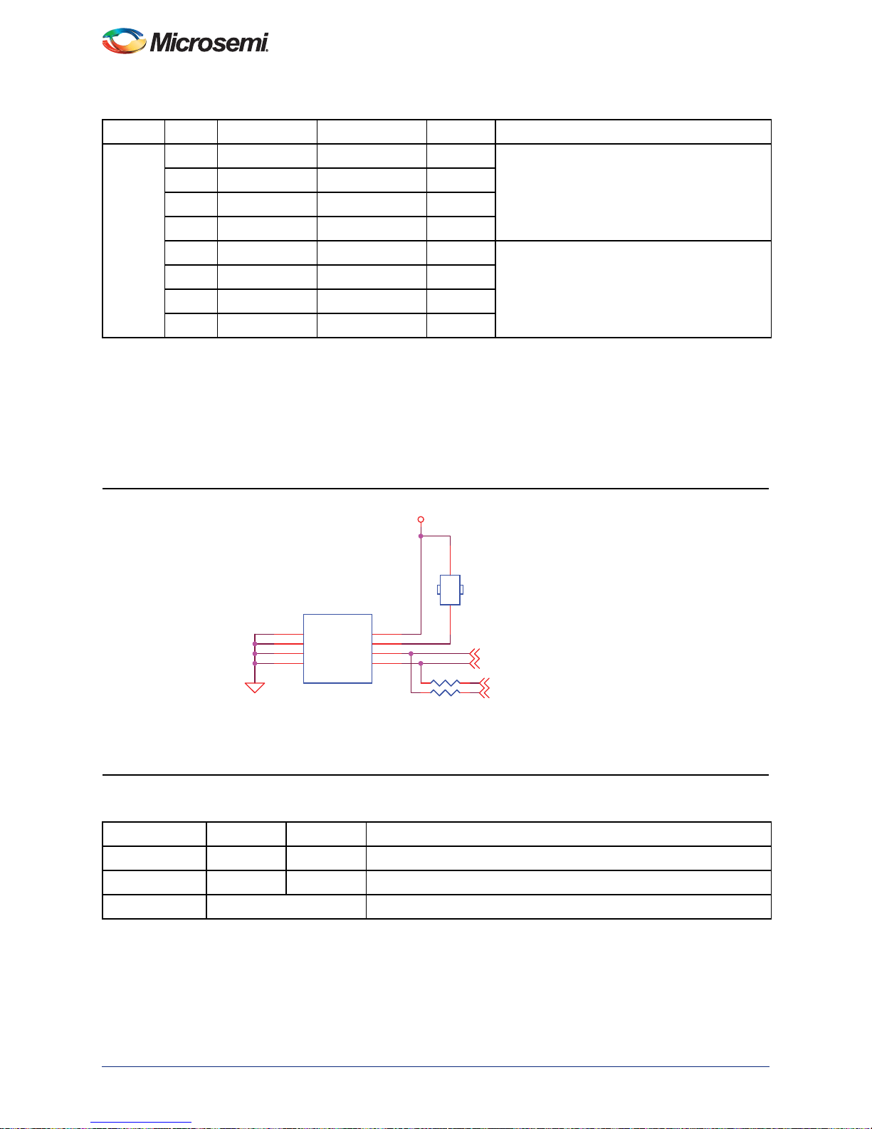
PWM Circuit
The PWM RC circuit depicted in Figure 3-3 and Figure 3-4 on page 21 can be used with Microsemi
CorePWM instantiated in the FPGA fabric to generate various voltage waveforms. These voltage
waveforms can be displayed on the OLED or used via the mixed signal header. In addition, one PWM RC
circuit source is routed to the AV input pin of an analog quad. This AV pin can be used to monitor the
generated voltage with high accuracy, depending on the ADC resolution configured in the FPGA fabric.
CURRENT MONITORING
AT0
2
1
R6
50K
50K
R6
AC0
100,1%
100,1%
R7
R7
5.36k
5.36k
S5BC-13-F
S5BC-13-F
D22
D22
V3P3
20 Revision 7
Page 21
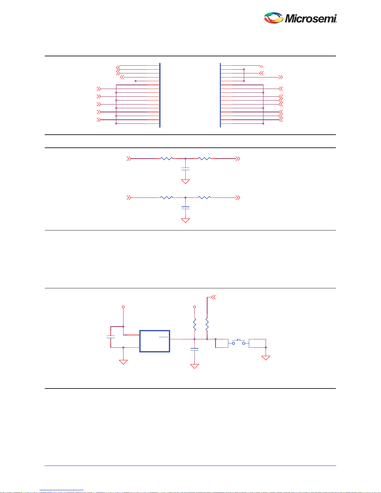
Figure 3-3 shows the A2F500 pins driving PWM and the PWM circuit.
PWM0 PWM1
F2-200-IO_8
F2-200-IO_6
F2-200-IO_7
DACOUT0{6}
AC4{6}
AC2{6}
AC3{6}
AV1_1{6}
DACOUT1 {6}
AT2 {6}
AT3 {6}
AV2_1 {6}
ATGND1 {6}
AT4 {6}
ATGND2 {6}
F2-200-4-FPGAIO
F2-200-6-FPGAIO
35
F2-200-7-FPGAIO
37
F2-200 PWM0
39
DGND8
41
AGND1
43
OBD0
45
AGND3
47
AC2
49
AGND5
51
AC3
53
AGND6
55
AC4
57
AGND8
59
AV1_1
61
63
F2-200-5-FPGAIO
DGND7
36
F2-200-8-FPGAIO
38
F2-200 PWM1
40
DGND9
42
AGND2
44
OBD1
46
AGND4
48
AT2
50
ATGND1
52
AT3
54
AGND7
56
AT4
58
ATGND2
60
AV2_1
62
64
PWM0
PWM1
F2-200-PWM1
F2-200-PWM0
C284
220nF
C284
220nF
R3164.7K R3164.7K
C283
220nF
C283
220nF
R3144.7K R3144.7K
R289100K R289100K
R281
100K
R281
100K
V3P3
V3P3
MSS_SYSRESETB {8,9,15,20,21,27}
Mfr P/N :DS1818R-10+T&R
Mfr: Dallas
RST
Mfr P/N :EVQ-PAD04M
Panasonic - ECG
Notes;
R35 need to place at U15
1
2
3
4
SW8
EVQ-PAD04M
SW8
EVQ-PAD04M
VCC
2
GND
3
RST
1
U15
DS1818
U15
DS1818
R34
10K
R34
10K
C74
1uF
C74
1uF
C73
0.1uF
C73
0.1uF
R3539R35
39
Figure 3-3 • PWM Pins
SmartFusion Development Kit
Figure 3-4 • PWM Circuit
Push-Button System Reset
A push-button system reset switch with a Schmitt trigger is provided on the board (Figure 3-5). The
Schmitt trigger reduces noise on the system reset push-button. SmartFusion MSS reset is synchronized
with this reset.
Figure 3-5 • Push-Button System Reset
Revision 7 21
Page 22
Components Description and Operation
V3P3
V3P3
V3P3
V3P3
V3P3
SWITCH1
SWITCH2
SWITCH4
SWITCH5
SWITCH3
Mfr P/N :KSC403J 50SH LFG
Panasonic - C&K Components
Mfr P/N :KSC403J 50SH LFG
Panasonic - C&K Components
Mfr P/N :KSC403J 50SH LFG
Panasonic - C&K Components
Mfr P/N :KSC403J 50SH LFG
Panasonic - C&K Components
Mfr P/N :KSC403J 50SH LFG
Panasonic - C&K Components
1
2
3
4
SW1
KSC403J 50SH LFG
SW1
KSC403J 50SH LFG
R46
10K
R46
10K
1 2
3 4
SW2
KSC403J 50SH LFG
SW2
KSC403J 50SH LFG
R48
10K
R48
10K
1 2
3 4
SW4
KSC403J 50SH LFG
SW4
KSC403J 50SH LFG
1 2
3
4
SW5
KSC403J 50SH LFG
SW5
KSC403J 50SH LFG
R47
10K
R47
10K
1 2
3 4
SW3
KSC403J 50SH LFG
SW3
KSC403J 50SH LFG
R44
10K
R44
10K
R43
10K
R43
10K
Push-Button, DIP Switches, and User LEDs
Push-button switches and user LEDs can also be used for debugging and for various applications, such
as gaming.
Figure 3-6 • Test LEDs
The board provides users access to four active Low LEDs, which are connected to the SmartFusion pins
B19, B20, C19, and H17.
LED1_N
LED2_N
LED3_N
LED4_N
R32 1.5KR32 1.5K
R38 1.5KR38 1.5K
R40 1.5KR40 1.5K
R41 1.5KR41 1.5K
Mfr P/N :SML-512DWT86
Mfr: Rohm
D1
D1
LED_ORANGE
LED_ORANGE
D2
D2
LED_ORANGE
LED_ORANGE
D3
D3
LED_ORANGE
LED_ORANGE
D4
D4
LED_ORANGE
LED_ORANGE
ACTIVE LOW
V3P3
Figure 3-7 • Push-Button Switches
22 Revision 7
The board comes with Two four input DIP switches.
Page 23
The inputs of AGLP_DIP switch are connected to pins N13,P16,R2,T2 of Bank 2 of the AGLP125
AGLP_3.3V_SIG1AGLP_3.3V_SIG1
AGLP_3.3V_SIG2AGLP_3.3V_SIG2
AGLP_3.3V_SIG3AGLP_3.3V_SIG3
AGLP_3.3V_SIG4AGLP_3.3V_SIG4
1
2
4
J20
HEADER 2X2
3
AGLP_3.3V_DIP1AGLP_3.3V_DIP1
AGLP_3.3V_DIP2AGLP_3.3V_DIP2
AGLP_3.3V_DIP3AGLP_3.3V_DIP3
AGLP_3.3V_DIP4AGLP_3.3V_DIP4
AGLP_DIP
R158
R161
R163
R164
4.7K
4.7K
4.7K
4.7K
AGLP_DIP
S2
V3P3
5
6
7
8
Mfr P/N: 76SB04ST
Mfr: GrayhillInc
2
3
4
1
CS289.
Figure 3-8 • AGLP_ DIP
The inputs of A2F_ DIP switch are connected to pins H20, C21, D21, and F19 of the
SmartFusion cSoC.
SmartFusion Development Kit
V3P3
R33 4.7KR33 4.7K
R36 4.7KR36 4.7K
R37 4.7KR37 4.7K
R39 4.7KR39 4.7K
1
2
3
4
Mfr P/N :76SB04ST
Mfr: Grayhill Inc
Figure 3-9 • Input Push-Button Switch
In addition, the board includes five push-button switches that are connected to pins G19, G20, G21, E1,
and F14 of the SmartFusion cSoC.
U7-17
U7-17
LED1_N
LED2_N
LED3_N
LED4_N
DIP1
DIP2
DIP3
B19
GBB0/IO18NDB0V0
B20
GBB1/IO18PDB0V0
C19
GBA0/IO19NPB0V0
H17
IO25NDB1V0
H20
GCC0/IO26NPB1V0
C21
GBC2/IO21PDB1V0
D21
IO21NDB1V0
F2-200/500-FGG484
F2-200/500-FGG484
Figure 3-10 • LED, DIP, and Push-Button I/Os
S1
8
7
6
5
A2F_DIPS1A2F_DIP
LED , DIP & PB
LED , DIP & PB
GCA2/IO23PDB1V0
GCB2/IO24PDB1V0
GFC2/IO67PPB5V0
GBC0/IO17NPB0V0
IO23NDB1V0
IO24NDB1V0
DIP1
DIP2
DIP3
DIP4
F19
G19
G20
G21
E1
E14
DIP4
SWITCH1
SWITCH2
SWITCH3
SWITCH4
SWITCH5
Revision 7 23
Page 24
Components Description and Operation
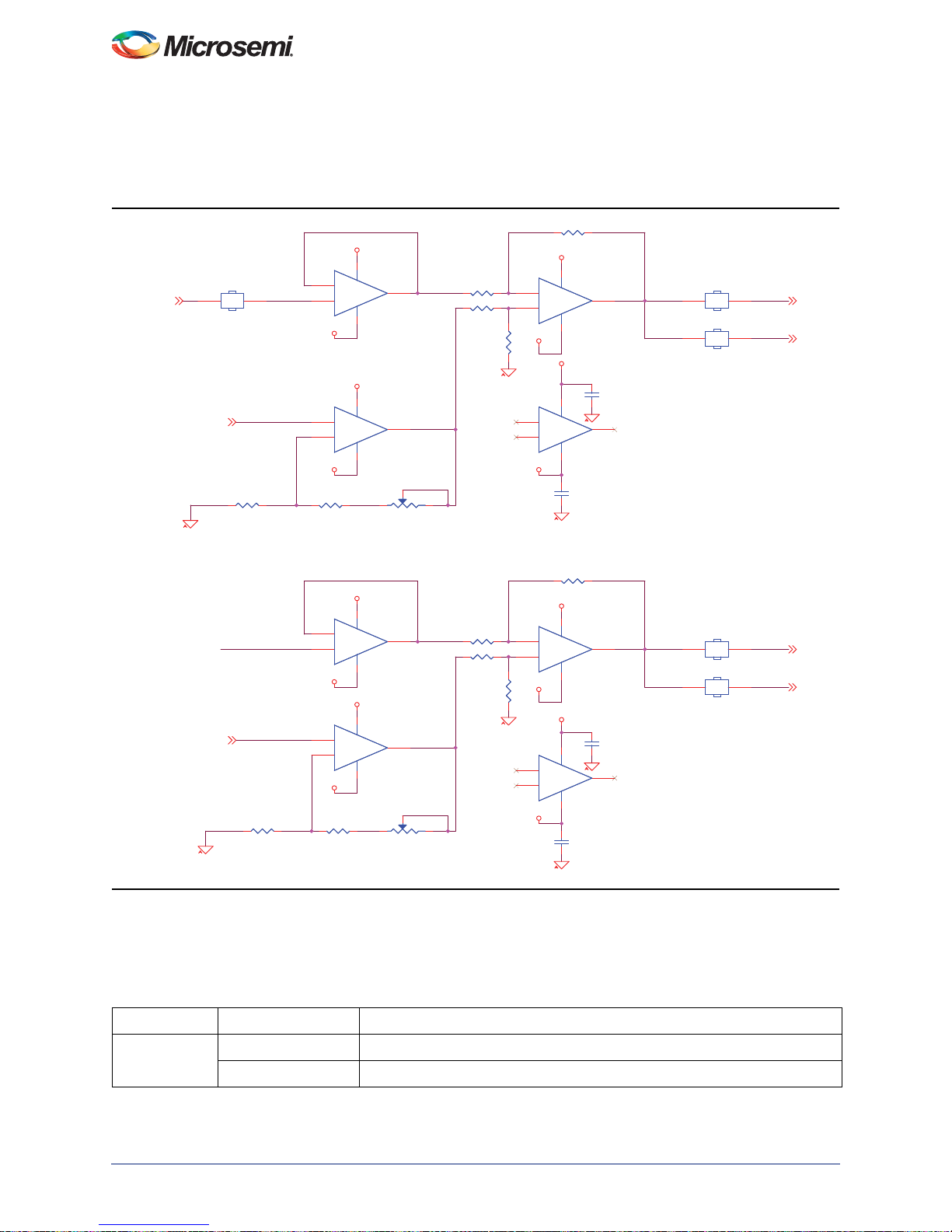
One-Bit DAC (OBD) Circuit
For applications that require conversion from a digital to analog domain , two analog conditi oning circui ts
are provided. This is useful in closed-loop applications. Figure 3-11 shows the circuit. Table 3-5 on
page 25 and Table 3-6 on page 26 show the jumper settings.
VAREF_OUT{6}
OBD_DACOUT0
{6}
AGND
OBD_DACOUT1{6}
AGND
JP13
JP13
12
HEADER 1x2
HEADER 1x2
R140 1K,1%R140 1K,1%
VREF_OUT
R151 1K,1%R151 1K,1%
VREF_OUT
1P15V
U44A
U44A
2
-
-
3
+
+
1N15V
1P15V
U44B
U44B
5
+
+
6
-
-
1N15V
R139 500,1%R139 500,1%
1P15V
U51A
U51A
2
-
-
3
+
+
1N15V
1P15V
U51B
U51B
5
+
+
6
-
-
1N15V
R152 500,1%R152 500,1%
411
AD824ARZ-14
AD824ARZ-14
AD824ARZ-14
AD824ARZ-14
11 4
1 3
411
AD824ARZ-14
AD824ARZ-14
AD824ARZ-14
AD824ARZ-14
11 4
1 3
R147 5.8K,1%R147 5.8K,1%
1P15V
411
U44C
U44C
AGND
R178
R178
5.8K,1%
5.8K,1%
10
13
12
9
-
-
+
+
AD824ARZ-14
AD824ARZ-14
1N15V
MANUFACTURER P/N = AD824ARZ-14
MANUFACTURER P/N = AD824ARZ-14
1P15V
MANUFACTURER = Analog Devices Inc
MANUFACTURER = Analog Devices Inc
C161
C161
411
U44D
1N15V
U44D
-
-
+
+
AD824ARZ-14
AD824ARZ-14
C162
C162
0.01uF
0.01uF
0.01uF
0.01uF
8
AGND
14
1
7
2
1K
R21 1K,1%R21 1K,1%
R22 1K,1%R22 1K,1%
RV21KRV2
JP14
JP14
JP15
JP15
12
HEADER 1x2
HEADER 1x2
12
HEADER 1x2
HEADER 1x2
AV1_0 {6}
AV1_2 {6}
AGND
R148 5.8K,1%R148 5.8K,1%
1P15V
411
U51C
U51C
AGND
R179
R179
5.8K,1%
5.8K,1%
9
-
-
10
+
+
AD824ARZ-14
AD824ARZ-14
1N15V
1P15V
411
U51D
U51D
13
-
-
12
+
+
AD824ARZ-14
AD824ARZ-14
MANUFACTURER P/N = AD824ARZ-14
MANUFACTURER P/N = AD824ARZ-14
1N15V
MANUFACTURER = Analog Devices Inc
MANUFACTURER = Analog Devices Inc
C163
C163
0.01uF
0.01uF
8
C164
C164
0.01uF
0.01uF
AGND
14
1
7
2
R149 1K,1%R149 1K,1%
R150 1K,1%R150 1K,1%
RV31K RV31K
JP21
JP21
JP27
JP27
12
HEADER 1x2
HEADER 1x2
12
HEADER 1x2
HEADER 1x2
AV2_0 {6}
AV2_2 {6}
AGND
Figure 3-11 • OBD_DACOUT
The OBDs can be used in two applications.
These circuits take the OBD output of the SmartFusion quad and feed it back to the SmartFusion analog
inputs of ADC0 and ADC1 (Table 3-3). This is useful in closed-loop applications.
Table 3-3 • OBD Output to Loopback to ADC
Jumper Pin Function
JP4 3-4 DACOUT0 to ADC0
7-8 DACOUT1 to ADC1
24 Revision 7
Page 25
SmartFusion Development Kit
The OBDs can also be fed into a voltage gain circuit as shown in Figure 3-11 on page 24 and described
in Table 3-4. In this application, the OBD sweep of 0–2.56 V can be translated to –15 V to +15 V. This is
useful in closed-loop applications for ABPS channels with prescalers.
Table 3-4 • OBD Connections for Voltage Gain
Jumper Pin Pin
JP4 1–3 DACOUT0 to OBD_DACOUT0
7–9 DACOUT1 to OBD_DACOUT1
JP13 1–2 Connect VAREF_OUT to bias the opamp
The output of the Opamp can be configured to be monitored by the ABPS channel (Table 3-5). This can
be done as below:
Table 3-5 • Output of the Opamps to ABPS Channels
Jumper Pin Pin Function
JP14 1 2 OP_AMP (U44C) output to ABPS0 of FPGA fabric
JP15 1 2 OP_AMP (U44C) output to ABPS4 of FPGA fabric
JP21 1 2 OP_AMP (U51C) output to ABPS1 of FPGA fabric
JP27 1 2 OP_AMP (U51C) output to ABPS5 of FPGA fabric
OLED Display
A 9616-pixel low-power OLED is made available on the board for display. This low-power device, WHITE
OLED, requires 3.3 V and 10 V power supplies. Either one of the SmartFusion MSS I2C0 or SPI0 can be
interfaced with the OLED.
The OLED displays sharp gaming images or text. For example, the SmartFusion RTC current time or
time between two events can be displayed on the OLED. Figure 3-12 on page 26 shows the OLED
connections on the board along with jumpers for BS1 and BS2 and the jumper settings for accessing the
OLED from SPI0.
Revision 7 25
Page 26
Components Description and Operation
OLED_BS1 OLED_BS2
OLED_BS1 OLED_BS2
OLED_CS#
V3P3
V3P3 V3P3
V10P
V3P3
OLED_D/C#{27}
MSS_SYSRESETB{8,12,15,20,21,27}
OLED_SCL {10}
OLED_SDA_OUT {10,11}
OLED_SDA_IN {10}
OLED_CS#
{11}
SCL
SDA
Mfr P/N :PMO13701
Mfr: PACER
Mfr P/N :3-644456-3
Mfr:Tyco Electronics
Mfr P/N :3-644456-3
Mfr:Tyco Electronics
TANT
R202MR20
2M
+
C67
4.7uF 25V
+
C67
4.7uF 25V
C68
0.01uF
C68
0.01uF
R201
10K
R201
10K
R17
10K
R17
10K
1
2
3
JP22JP22
R202
10K
R202
10K
R1651KR165
1K
R203
10K
R203
10K
R18
10K
R18
10K
1
2
3
JP23JP23
R3651KR365
1K
R207
10K
R207
10K
R19
10K
R19
10K
C69
1uF
C69
1uF
VCC
30
VCOMH
29
IREF
28
VDD
11
BS1
12
BS2
13
NC11NC28NC39NC410NC514NC6
31
VSS
2
TEST1
7
TEST2
6
TEST3
5
TEST4
4
TEST5
3
D0
20
D1
21
D2
22
D3
23
D4
24
D5
25
D6
26
D7
27
RD#
19
WR#
18
D/C#
17
RES#
16
CS#
15
U11
PMO13701
U11
PMO13701
Refer to the "Jumper Settings" section on page 26 for accessing the OLED from I2C0 and SPI0.
Figure 3-12 • OLED Connections
Jumper Settings
Table 3-6 • Interface MSS I2C0 to the OLED
Jumper Pin Pin Connection Details
J7 2 3 I2C_0_SCL to OLED_SCL
14 15 I2C_0_SDA to OLED_SDA_IN
JP18 1 2 Closed
JP23 1 2 OLED_BS1 connected to 3.3 V
JP22 2 3 OLED_BS2 connected to GND
Table 3-7 • Interface MSS SPI0 to the OLED
Jumper Pin Pin Connection Details
J7 3 4 SPI_SCK to OLED_SCL
JP8 1 2 SPI_0_OUT to OLED_SDA_IN
JP18 1 2 Open
JP23 2 3 OLED_BS1 connected to GND
JP22 2 3 OLED_BS2 connected to GND
26 Revision 7
15 16 SPI_SDA to OLED_SDA
5 6 SDI_0_IN to OLED_SDA_OUT
9 10 SCLK_0_OUT to OLED_SCL
13 14 SS_0_OUT to OLED_CS#
Page 27
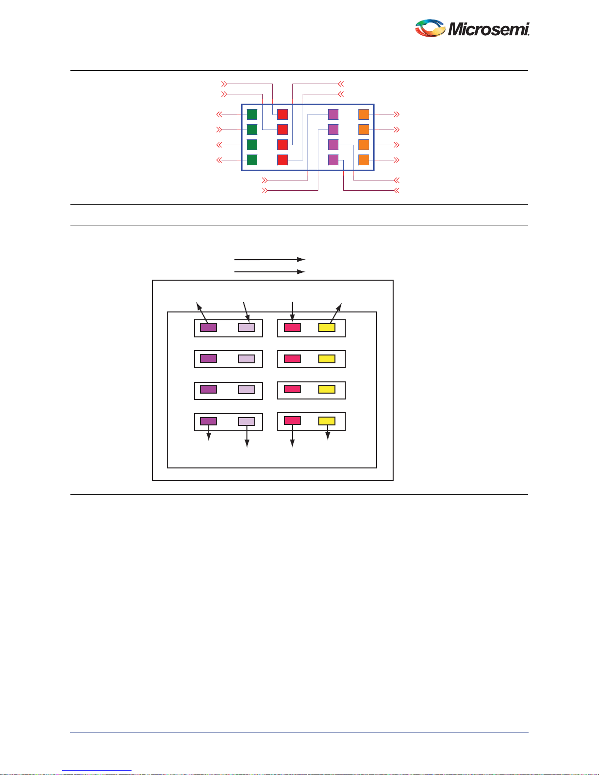
Figure 3-13 • JP8 Jumper Details
OLED_CS#
{9}
SPI_0_SCK
{10}
SDO_0_OUT
SDI_0_IN
SCLK_0_OUT
SS_0_OUT
SS_1_OUT
SCLK_1_OUT
SPI_1_SO
SPI_1_SI
SPI_1_SCK
SPI_CS_N
SDI_1_IN
SDO_1_OUT
SPI_0_SI
{10}
OLED_SDA_OUT{9,10}
2
3
4
6
7
8
10
11
12
14
15
16
1
5
9
13
JP8
HDR4X4
JP8
HDR4X4
SPI Configuration –1
SPI Port 0
SPI Port 1
OLED
SPI Flash
OLED
Display
SPI
Port 0
SPI
Port 1
SPI
Flash
OLED
Display
SPI
Port 0
SPI
Port 1
SPI
Flash
SmartFusion Development Kit
Figure 3-14 • MSS SPI0 and SPI1 Settings
Revision 7 27
Page 28
Components Description and Operation
SPI_SO
V3P3
V3P3
SPI_CS_N
SPI_1_SI
SPI_1_SCK
SPI_1_SO
8 MByte
Mfr P/N : AT25DF641-MWH-T
Mfr: Atmel
R28
10K
R28
10K
R293
10K
R293
10K
SI
5
SCK
6
HOLD
7
CS
1
WP
3
VCC
8
GND
4
SO
2
U13
AT25DF641-MWH-T
U13
AT25DF641-MWH-T
C70
0.1uF 10V
C70
0.1uF 10V
R206 39R206 39
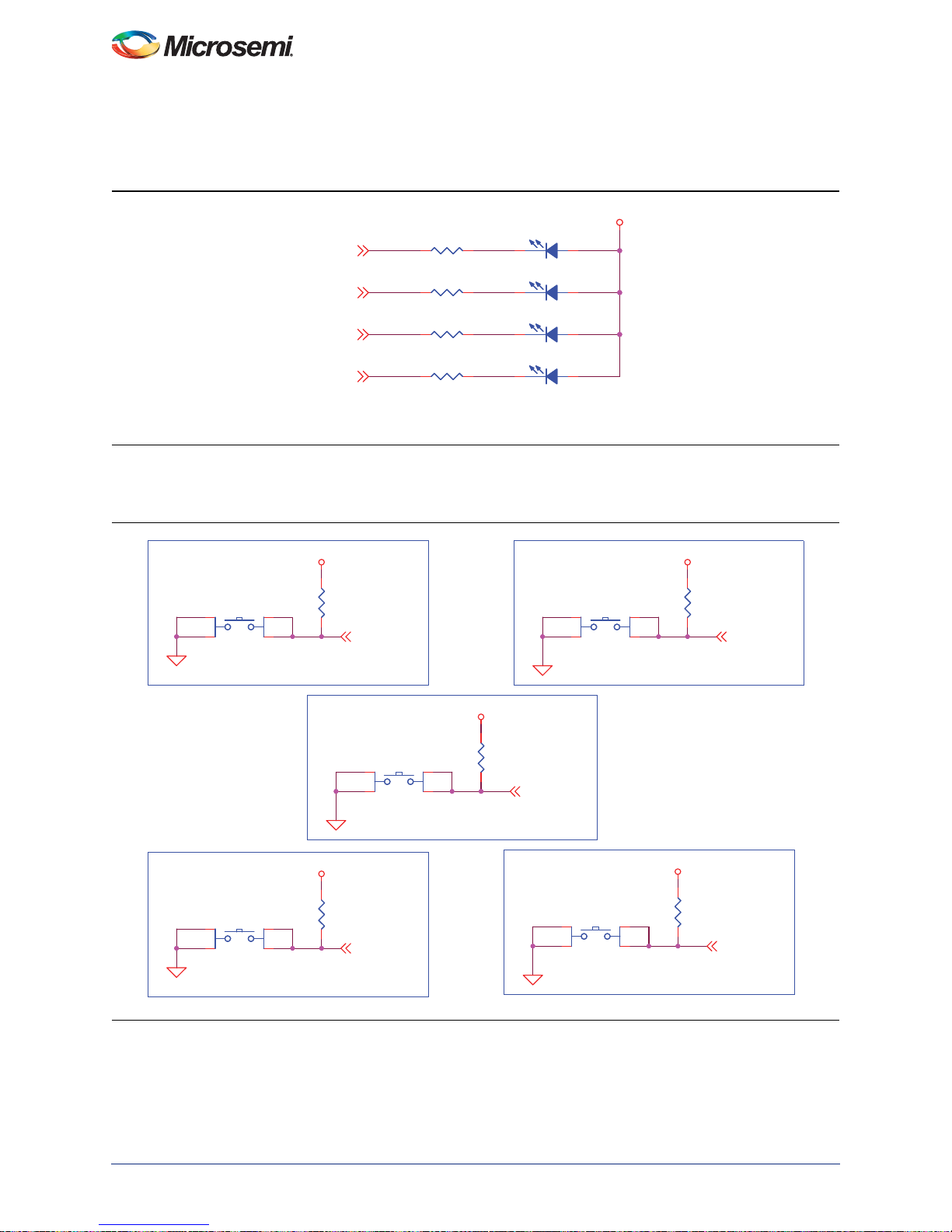
Table 3-8 • MSS SPI0 and MSS SPI1 Loopback and Off-Board SPI Device Connections
Jumper Pin Signal Connection Details
JP8 6 SPI0_SDI To interface any SPI device to MSS SPI0
2 SPI0_SDO
10 SPI0_SCK
14 SPI0_SS
3 SPI1_SDI To interface any SPI device to MSS SPI1
7 SPI1_SDO
11 SPI1_SCK
15 SPI1_SS
6 7 MSS SPI0 and SPI1 loopback
23
10 11
14 15
SPI Flash
One 8-MByte SPI flash Atmel AT25DF641-MWH-T is also offered on the board. This can optionally be
interfaced to either the SPI0 or SPI1 peripherals of the SmartFusion MSS. Figure 3-15 and Figure 3-16
show the SPI flash circuit and the jumper settings to access it from SPI1.
Figure 3-15 • SPI Flash
Table 3-9 • MSS SPI1 to SPI Flash
Jumper Pin Pin Connection Details
JP8 3 4 SDI_1_IN to SPI_1_SO (SO output of SPI flash)
7 8 SDO_1_OUT to SPI_1_SI (SI input of SPI flash)
11 12 SCLK_1_OUT to SPI_1_SCK (SCK input of SPI flash)
15 16 SS_1_OUT to SPI_CS_N (CS# input of SPI flash)
28 Revision 7
Page 29
SPI DAC
One 12-bit SPI DAC AD5320 is available on the board. This can be optionally interfaced to either the
SPI0 or SPI1 of the SmartFusion MSS. Figure 3-16 shows the SPI DAC instance along with the header
that must be connected to the SPI_x_SDI, SPI_x_SCK, SPI_x_SS, and SPI_x_SDO pins of SPI0 or
SPI1.
HEADER 1
HEADER 1
HEADER 1
HEADER 1
HEADER 1
HEADER 1
J16
J16
J17
J17
J18
J18
SmartFusion Development Kit
V3P3
C72
ANA_V
C72
10uF 16V
10uF 16V
JP3
JP3
1
HEADER 1x2
HEADER 1x2
2
C71
C71
3
U14
U14
1
1
1
R30
R30
R31
R31
50 NL
50 NL
50 NL
50 NL
R29
R29
50 NL
50 NL
4
DIN
VDD
5
6
SCLK
SYNC
VOUT
GND
AD5320_NL
AD5320_NL
2
0-1uF 10V
0-1uF 10V
1
Figure 3-16 • SPI DAC
Revision 7 29
Page 30
Components Description and Operation
I2C_WC_N
V3P3
I2C_EEPROM_SCL
I2C_EEPROM_SDA
ET1100_I2C_EEPROM_SCL {31}
ET1100_I2C_EEPROM_SDA {31}
Device Select Code: " 0 0 0 "
R309 0R309 0
12
JP26
HEADER 1x2
JP26
HEADER 1x2
R307 0R307 0
E0
1
E1
2
E2
3
VSS
4
SDA
5
SCL
6
WC_N
7
VCC
8
U12
M24512-WMN6TP
MANUFACTURER P/N = M24512-WMN6TP
MANUFACTURER = STMicroelectronics
U12
M24512-WMN6TP
MANUFACTURER P/N = M24512-WMN6TP
MANUFACTURER = STMicroelectronics
Table 3-10 • To Interface MSS SP10 or MSS SPI1 to SPI DAC
Jumper Pin Signal Header/Jumper Signal Connection Detai ls
JP8 6 SPI0_SDI J16 DIN To Interface SPI DAC to MSS SPI0
2 SPI0_SDO JP3 (Pin1) VOUT
10 SPI0_SCK J17 SCK
14 SPI0_SS J18 SYNC#
3 SPI1_SDI J16 DIN T o Interface SPI DAC to MSS SPI1
7 SPI1_SDO JP3 (Pin1) VOUT
1 1 SPI1_SCK J17 SCK
15 SPI1_SS J18 SYNC#
I2C EEPROM
One 512-Kbit I2C EEPROM ST M24512-WMN6TP is available on the board to interface with I2C Port1 of
the SmartFusion MSS. Alternatively the EtherCAT chip, Beckhoff ET1100, can interface with the
EEPROM.
Figure 3-17, and Figure 3-18 and Figure 3-19 on page 31 show the EEPROM connections, I2C interface,
and header with jumper settings for access to EEPROM.
Figure 3-17 • I2C EEPROM
Table 3-11 • To Interface MSS I2C1 to EEPROM
Jumper Pin Pin Connection Details
J7 6 7 I2C_1_SCL to EEPROM_SCL
14 15 I2C_1_SDA to EEPROM_SDA
JP26 Closed To write protect EEPROM (WE_N)
30 Revision 7
Page 31

SmartFusion Development Kit
SPI_0_SCK {11}
SPI_0_SI {11}
I2C_SCL_0_IN
I2C_SCL_1_IN
I2C_SDA_1_IN
I2C_SDA_0_IN
OLED_SCL {9}
I2C_EEPROM_SDA
OLED_SDA_IN {9}
I2C_EEPROM_SCL
1
5
9
13
14415
7
11
16
3
2
10 6
8
12
J7
I2C INTERFACE
J7
I2C INTERFACE
Figure 3-18 • MSS I2C0 and I2C1 Jumper Settings
Table 3-12 • To Interface EtherCAT ET1100 to EEPROM
EEPROM PIN ET1100 PIN Connection details Comment
5 G11 EEPROM CLK of ET1100 to SCL of EEPROM When MSS I2C1 is not
6 F11 EEPROM DATA of ET1100 to SDA of EEPROM
driving EEPROM
JP26 Closed To write protect EEPROM (WE_N)
V3P3
R24
Figure 3-19 • I
I2C_SDA_0_IN
I2C_SCL_0_IN
I2C_SDA_1_IN
I2C_SCL_1_IN
2
C Interface Terminations
R23
R23
10K
10K
R24
10K
10K
R25
R25
10K
10K
R26
R26
10K
10K
U7-16
U7-16
I2C INTERFACE
I2C INTERFACE
V21
I2C_0_SDA/GPIO_22
U21
I2C_0_SCL/GPIO_23
V22
I2C_1_SDA/GPIO_30
U20
I2C_1_SCL/GPIO_31
F2-200/500-FGG484
F2-200/500-FGG484
PORT0
PORT0
PORT1
PORT1
Revision 7 31
Page 32

Components Description and Operation
V3P3
V3P3
CLK_50MHZ {27}
MSS_RMII_CLK {15}
E/D
1
GND
2
VDD
4
OUTPUT
3
Y3
50Mhz_HC73
Y3
50Mhz_HC73
R231 39R231 39
C75 0.01uFC75 0.01uF
R45 39R45 39
R42 10KR42 10K
PTBASE
V1P5_INTV1P5_INTV1P5_INT
RTC_SW
Mfr P/N :EVQ-PAD04M
Mfr: Panasonic - ECG
RESET CIRCUIT
AGND AGND
AGND AGND
U7-2
F2-500-FGG484
U7-2
F2-500-FGG484
PCAP
AB5
NCAP
AB6
PU_N
W17
PTBASE
AB20
PTEM
Y18
MAINXIN
AA16
LPXIN
AA18
MAINXOUT
AA17
LPXOUT
AA19
C49
2.2uF 16V
C49
2.2uF 16V
12
C51
30pF
C51
30pF
C53
0.1uF
C53
0.1uF
C52
30pF
C52
30pF
C48
18pF
C48
18pF
SW7
EVQ-PAD04M
SW7
EVQ-PAD04M
12
34
C50
18pF
C50
18pF
Y2
32.768 KHZ
Y2
32.768 KHZ
Y1
20MHZ 20 PPM
Y1
20MHZ 20 PPM
Clock Oscillator
A 50 MHz cloc k oscillator with 20 PPM is available on the board (Figure 3-20). This cl ock oscillator is
connected to the FPGA fabric to provide a system reference clock and connected to the PHY to provide
the RMII_CLK. An on-chip SmartFusion PLL can be configured to generate a wide range of highprecision clock frequencies.
Figure 3-20 • 50 MHz RC OSC
20 MHz Oscillator
A 20 MHz resonator o f 20 PPM is placed across the MAINXIN and MAINXOUT pins of the SmartFusion
cSoC with the appropriate 18 pF capacitors. This is used to generate high precisio n clock for Ethernet
MAC and also in RTC based applications.
32.768 KHz (low power) Oscillator
A 32.768 KHz resonator, CM519, is placed across the LPXIN and LPXOUT pins of the SmartFusion
cSoC with the appropriate 30 pF capacitors. This low-power resonator is useful in RTC based
applications.
Figure 3-21 • 20 MHz and 32.768 KHz Oscillators
32 Revision 7
Page 33

SmartFusion Development Kit
USB-to-UART Interface
Included on the development board is a USB-to-UART interface with ESD protection (Figure 3-22). This
interface includes an integrated USB-to-UART bridge controller (U16) to provide a standard UART
connection with the SmartFusion MSS UART0 port.
One application of the USB-to-UART interface is to allow HyperTermina l on a PC to communicate with
the SmartFusion cSoC. HyperTerminal is a serial communications application program that can be
installed in the Windows
Windows.
With a USB driver properly installed, and the correct COM port and communication settings selected, you
can use the HyperTerminal program to communicate with a design running on the SmartFusion cSoC.
Table 3-13 lists the supported UART parameters, such as baud rate, for HyperTerminal application.
Table 3-13 • UART HyperTerminal Settings
Supported HyperTerminal Parameters
Baud Rates Data Bits Parity Types STOP BIT
110 5, 6, 7, 8 NO/ODD/EVEN/MARK (1)/SPACE (0) ONE/ONE-HALF/TWO
300
1200
2400
®
operating system. A basic HyperTe rminal program is usually distributed with
4800
9600
19200
38400
57600
115200
230400
460800
921600
TXD_0_OUT
RXD_0_IN
R236 39R236 39
U7-9
U7-9
UART INTERFACE
UART INTERFACE
Y22
UART_0_TXD/GPIO_20
U18
UART_0_RXD/GPIO_21
F2-500-FGG484
F2-500-FGG484
PORT0
PORT0
Figure 3-22 • USB-to-UART
Revision 7 33
Page 34

Components Description and Operation
V3P3
RXD_1_IN
RS485_B
RS485_A
TXD_1_OUT
RS485_DE
RS485_RE
R28839R288
39
R566
120
R566
120
R
D
U56
MAX3430CSA
R
D
U56
MAX3430CSA
R0
1
RE
2
DE
3
DI
4
VCC
8
B
7
A
6
GND
5
C81
0.1uF
C81
0.1uF
RS485_RE
RS485_DE
RXD_1_IN
TXD_1_OUT
R28739R287
39
UART HANDSHAKING
PORT1
U7-18
F2-500-FGG484
UART HANDSHAKING
PORT1
U7-18
F2-500-FGG484
GDA2/IO42NDB1V0
L18
GDB1/IO39PDB1V0
L20
UART_1_TXD/GPIO_28
V20
UART_1_RXD/GPIO_29
W22
RS485 Interface
Included on the development board is an RS485 with DB9 female connector, interfacing with the
MAX3240CSA connected to UART port 1 (Figure 3-23, Figure 3-24, and Figure 3-25 on page 35) of the
SmartFusion MSS. This is provided for applications that require RS485, for which the UART port needs
to be used in MODEM mode.
Figure 3-23 • RS485
Figure 3-24 • SmartFusion UART Port 1
34 Revision 7
Page 35

P1
P1
1
6
SmartFusion Development Kit
11
G3
DCD
DSR
Figure 3-25 • DB9 Connector
Ethernet Interface
One Ethernet interface, configured for RMII full d uplex mode, and a low-powe r 10/100 Mbps single-port
Ethernet physical layer transceiver (U19) are provided on-board (Fig ure 3-27 on page 36). The Ethernet
physical layer features integrated sub-layers to support both 10BASE-T and 100BASE-TX Ethernet
protocols. These sub-layers ensure compatibility and interoperability with many other standards-based
Ethernet solutions.
The Ethernet RJ45 interface and physical layer, the interface with the SmartFusion MSS Ethernet media
access controller (MAC) which supports RMII, serves many purposes. For example, this interface can be
used to access the SmartFusion cSoC to monitor the ADC data over a network. The embedded system
memory and control registers can be accessed and processed remotely to support system management.
RS485_B
RS485_A
2
TX
7
RTS
3
RX
8
CTS
4
DTR
9
RI
5
G1
G2
CONNECTOR DB9F
CONNECTOR DB9F
Manufacturer P/N = 152-3409
Manufacturer P/N = 152-3409
10
Manufacturer = Kobiconn
Manufacturer = Kobiconn
Clocking Scheme for RMII CLK
The 10/100 MAC RMII interface requires a 50 MHz clock. The PHY device also requires a 50 MHz
20 PPM clock for proper operation. While there are a few possible ways of providing the clock, the
following two schemes are discussed:
Clocking Scheme 1: From 50 MHz clock oscillator
• 50 MHz oscillator goes as input to CCC and to the X1 clock input of Ethernet PHY through GPIO
• The GLC output of CCC, which is also at 50 MHz, feeds MAC_CLK of 10/100 MAC
Revision 7 35
Page 36

Components Description and Operation
Clocking Scheme 2: From 20 MHz clock oscillator
• 20 MHz oscillator goes as input to CCC. GLC output of CCC is configured at 50 MHz
• The GLC output of CCC feeds MAC_CLK of 10/100 MAC
• The same GLC output of CCC feeds X1 clock input of Ethernet PHY through GPIO
Clock Conguration 1
A2F500
X1 Input
50 MHz OSC
Clock Conguration 2
20 MHz OSC
Figure 3-26 • Ethernet Clocking
FPGA_ENA_MDC
FPGA_ENA_MDIO
FPGA_ENA_TXEN
FPGA_ENA_TXD0
FPGA_ENA_TXD1
22
22
R24222R242
R23322R233
R23422 R23422
CCC
50 MHz
GLC
A2F500
CCC
GLC
50 MHz
U7-14
AA3
MAC_MDC/IO57RSB4V0
V4
MAC_MDIO/IO58RSB4V0
Y4
MAC_TXEN/IO61RSB4V0
AA5
MAC_TXD[0]/IO65RSB4V0
W5
MAC_TXD[1]/IO64RSB4V0
10/100 MAC
MAC_CLK
10/100 MAC
MAC_CLK
ETHERNETETHERNET
MAC_CRSDV/IO60RSB4V0
MAC_RXER/IO59RSB4V0
MAC_RXD[0]/IO63RSB4V0
MAC_RXD[1]/IO62RSB4V0
TXD
RXD
TXD
RXD
MAC_CLK
W4
AA4
V5
U5
T6
Ethernet
PHY
50 MHz Clk
Output
X1 Input
Ethernet
PHY
50 MHz Clk
Output
FPGA_ENA_CRS
FPGA_ENA_RXER
FPGA_ENA_RXD0
FPGA_ENA_RXD1
MSS_RMII_CLK {12}
Figure 3-27 • Ethernet Interface
36 Revision 7
F2-500-FGG484
Page 37

Memory Section Overview
Part Number
CY7C1061DV33–10ZSXI(1M X 16)
JS28F640J3D–75 (4M X 16)
Part#
MT45W8MW16BGX (8M X 16)
JS28F128P30T85873824 (16M X 16)
Logic 0 – All Out Buffers are tristated
Logic 1 – Channeling is in use
SRAM
and Flash
SRAM
SRAM
PSRAM
and
Flash
PSRAM
Flash
Flash
Flash
When memory is not used the
Expansion connector will be used
As 3.3V GPIOs
3.3 V
Interface
3.3 V
Interface
1.8 V
Interface
Expansion
Connector
0 Ohm
Isolation
Resistors
Design 1: GPIOs are channeled from
A2F500 to Expansion Header Pins
A2F500
AGLP
CS289
Design 2: GPIOs are channeled from
A2F500(EMC) to PSRAM/Header Pins
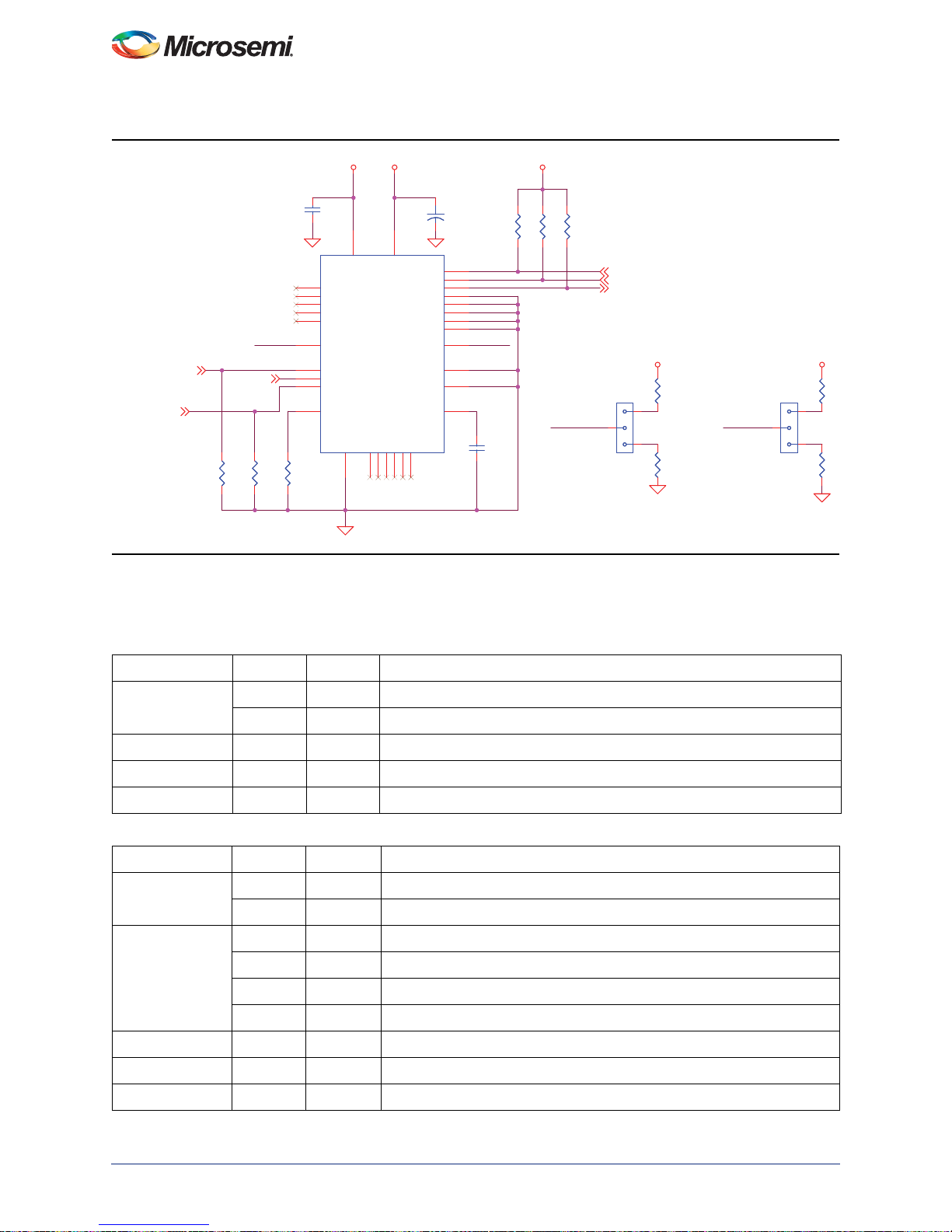
The SmartFusion MSS provides options to interface with a variety of external memory devices such as
NOR flash and synchronous or asynchronous SRAM for large applications co de. The external memory
controller (EMC) interface of SmartFusion MSS is 3.3 V LVTTL compliant. This interfaces directly with
3.3 V SRAM and flash devices. On the development board, two 16-Mbit SRAM Cypress
CY7C1061DV33-10ZSXI and two 64-Mbit parallel flash memory Numonyx JS28F640J3D-75 memories
interface with EMC region0 and region1. Microsemi expects these memories to be used in most
SmartFusion applications.
For applications that require larger SRAM memory than this, an alternative 128-Mbit, 1.8 V
asynchronous PSRAM Micron
only available at 1.8 V, coupled with the fact that the EMC interface does not allow region0 and region1 to
be completely independent of each other due to shared chip select, 128-Mbit, 1.8 V, parallel flash
memory Numonyx JS28F128P30T85 873824 is mounted on the board as a companion for the 1.8 V
SRAM. This requires a 3.3 V to 1.8 V conversion to interface the 3.3 V EMC with these 1.8 V memories.
If the EMC is not used, the shared EMC I/Os are available as 3.3 V GPIO at the expansion connector. To
provide the option of a 1.8 V interface and to make the EMC I/Os available to user application, an
AGLP125 FPGA is used as an I/O translator on the board. Based on the EMC configuration selected, the
AGLP125 can be programmed either as a 3.3 V to 1.8 V level converte r or I/O extender (with all 3.3 V
and 1.8 V memories held in tristate). This device can be selectively programmed by choosing appropriate
jumper settings to select the JTAG chain.
Figure 3-28 captures the memory section overview.
®
MT45W8MW16BGX is also offered. Given that memories of this size are
SmartFusion Development Kit
Figure 3-28 • Memory Top Level
Revision 7 37
Page 38

Components Description and Operation
3.3 V Memory Section
Mounted on the development board are two instances of 16-Mbit asynchronous SRAM. Also included are
two 64-Mbit parallel flash memories (FLASH). Both instances of the asynchronous SRAM are connected
to region0 of the EMC interface of the SmartFusion MSS. Similarly both instances of the flash are
connected to region1 of the EMC interface of the SmartFusion MSS. These operate at 3.3 V and are
directly interfaced to the EMC. The AGLP125 FPGA is not use d in this case and is he ld in Flash*Freeze
mode to avoid any power consumption.
Table 3-14 gives the summary of jumper settings needed to access the 3.3 V memories.
Table 3-14 • Jumper Settings to Interface EMC with 3.3 V Memories (SRAM and flash)
Jumper Pin Pin Connection Details
JP17 2 3 EMC chip select for region0 to CS1 of SRAM
JP19 2 3 EMC chip select for region1 to CS1 of flash
JP24 1 2 FLASH_VPEN to 3.3 V (to enable 3.3 V flash)
JP16 2 3 To keep AGLP125 in Flash*Freeze mode
Asynchronous SRAM Memory Components
The 3.3 V asynchronous SR AMs populated on the board are 16-Mb it SRAM Cypress CY7C1061DV3310ZSXI (PSRAM), as shown in Figure 3-29 on page 39. These interface with the EMC port of the
SmartFusion MSS. They provide a reasonable off-chip memory at high speed that the hard ARM
Cortex-M3 processor can use for applications such as RTOS.
Performance Note: Table 3-15 describes the External Memory Controller settings for 100 MHz and 80
MHz system performance. A slower speed device might work at higher speed—but it is not always
guaranteed. These are obtained on the development board with an application that uses asynchronous
SRAM extensively.
Tab le 3-15 • EMC Settings for 3.3 V Asynchronous SRAM Performance
Port Size: Half Word
Latency in FCLK(HCLK) Cycles
Read Latency for First Access 1 1
Read Latency for Remaining Accesses 1 1
Write Latency 0 0
Note: Make sure to keep AGLP125 device in Flash*Freeze mode by closing pins 2-3 of JP16.
System Clock Frequency FCLK (HCLK)
100 MHz 80 MHz
38 Revision 7
Page 39

SmartFusion Development Kit
V3P3
50
29
23
14
2
U21
U21
DATA0 {20,21,26}
DATA1 {20,21,26}
DATA2 {20,21,26}
DATA1
DATA2
DATA0
22
25
IO0
IO124IO2
VCC5
VCC4
VCC3
VCC2
VCC1
A0
A2
A1
9
10
11
ADDRESS1
ADDRESS3
ADDRESS2
ADDRESS1
ADDRESS2{20,21,26}
ADDRESS3
{20,21,26}
{20,21,26}
DATA0 {20,21,26}
DATA1 {20,21,26}
DATA4 {20,21,26}
DATA3 {20,21,26}
DATA5 {20,21,26}
DATA3
DATA4
DATA5
27
28
30
IO3
IO4
IO5
A38A4
A5
7
48
ADDRESS4
ADDRESS5
ADDRESS6
ADDRESS6
ADDRESS4
ADDRESS5{20,21,26}
{20,21,26}
{20,21,26}
DATA3 {20,21,26}
DATA4 {20,21,26}
DATA2 {20,21,26}
DATA6 {20,21,26}
DATA7 {20,21,26}
DATA8 {20,21,26}
DATA6
DATA7
DATA8
49
33
31
IO8
IO6
IO7
A845A944A10
A6
A7
47
46
ADDRESS9
ADDRESS7
ADDRESS8
ADDRESS7{20,21,26}
ADDRESS8{20,21,26}
ADDRESS9
{20,21,26}
DATA5 {20,21,26}
DATA6 {20,21,26}
DATA7 {20,21,26}
DATA9 {20,21,26}
DATA11 {20,21,26}
DATA10 {20,21,26}
DATA9
DATA10
DATA11
DATA12
52
51
1
54
IO9
IO11
IO10
A11
37
36
38
ADDRESS10
ADDRESS11
ADDRESS12
ADDRESS13
ADDRESS11
ADDRESS12
ADDRESS10{20,21,26}
{20,21,26}
{20,21,26}
DATA9 {20,21,26}
DATA10 {20,21,26}
DATA8 {20,21,26}
DATA12 {20,21,26}
DATA14 {20,21,26}
DATA13 {20,21,26}
DATA13
DATA14
3
IO12
IO144IO13
A1434A15
A13
A12
35
ADDRESS14
ADDRESS15
ADDRESS13{20,21,26}
ADDRESS14
ADDRESS15
{20,21,26}
{20,21,26}
DATA13 {20,21,26}
DATA11 {20,21,26}
DATA12 {20,21,26}
DATA15 {20,21,26}
DATA15
6
IO15
A17
A16
19
20
21
ADDRESS19
ADDRESS16
ADDRESS17
ADDRESS18
ADDRESS16{20,21,26}
ADDRESS17
ADDRESS18{20,21,26}
{20,21,26}
DATA14 {20,21,26}
DATA15 {20,21,26}
ADDRESS21 {20,21,26}
MCS_N_0
MBYTEN_0 {21,26}
MBYTEN_1 {21,26}
39
12
16
13
BLE
CE2
CE1
BHE
A19
A18
17
18
ADDRESS20
ADDRESS19{20,21,26}
ADDRESS20
{20,21,26}
SRAM1_ADDRESS21
MCS_N_0
MBYTEN_0 {21,26}
MBYTEN_1 {21,26}
40
NC243NC1
MANUFACTURER P/N = CY7C1061AV33-10ZXC
MANUFACTURER P/N = CY7C1061AV33-10ZXC
MANUFACTURER = Cypress Semiconductor
MANUFACTURER = Cypress Semiconductor
VSS5
53
VSS4
41
VSS3
32
VSS2
26
VSS1
5
OE
WE
42
15
CY7C1061AV33-10ZXC
CY7C1061AV33-10ZXC
MOE_N_0{21,26}
MRW_N{20,21,26}MOE_N_0{21,26}
V3P3
R2221KR222
23
Shunt b/w
JP17 pins
Memory Device
Config
3.3V INTERFACE
1.8V INTERFACE 1 2
MCS_N_0
MANUFACTURER P/N = 3-644456-3
MANUFACTURER = Tyco Electronics
MANUFACTURER P/N = 3-644456-3
MANUFACTURER = Tyco Electronics
JP17
JP17
123
1K
F2_MCS_N_0{21,26}
V3P3
Figure 3-29 • PSRAM Connections
50
29
23
14
2
U20
U20
DATA0
DATA1
DATA2
25
22
IO0
IO124IO2
VCC5
VCC4
VCC3
VCC2
VCC1
A0
A110A2
9
11
ADDRESS2
ADDRESS3
ADDRESS1
ADDRESS1
ADDRESS2
ADDRESS3
{20,21,26}
{20,21,26}
{20,21,26}
DATA3
DATA4
DATA5
28
27
IO530IO6
IO3
IO4
A548A6
A3
A4
7
8
ADDRESS4
ADDRESS5
ADDRESS6
ADDRESS4
ADDRESS5
ADDRESS6
{20,21,26}
{20,21,26}
{20,21,26}
DATA6
DATA7
DATA8
33
31
49
IO8
IO7
A7
A8
46
45
47
ADDRESS8
ADDRESS9
ADDRESS7
ADDRESS8
ADDRESS9
ADDRESS7
{20,21,26}
{20,21,26}
{20,21,26}
DATA10
DATA11
DATA9
DATA12
52
54
1
51
IO9
IO10
IO11
A11
A944A10
37
38
ADDRESS10
ADDRESS13
ADDRESS11
ADDRESS12
ADDRESS10
ADDRESS11
ADDRESS12
{20,21,26}
{20,21,26}
{20,21,26}
DATA13
DATA14
DATA15
3
6
IO144IO13
IO15
IO12
A15
A14
A1236A13
21
34
35
ADDRESS14
ADDRESS15
ADDRESS16
ADDRESS15
ADDRESS16
ADDRESS13
ADDRESS14
{20,21,26}
{20,21,26}
{20,21,26}
{20,21,26}
13
CE1
A16
A17
A18
18
20
19
ADDRESS18
ADDRESS19
ADDRESS20
ADDRESS17
ADDRESS18{20,21,26}
ADDRESS19
ADDRESS17
{20,21,26}
{20,21,26}
12
39
16
BLE
CE2
BHE
A19
17
ADDRESS20
{20,21,26}
43
40
V3P3
MANUFACTURER P/N = CY7C1061AV33-10ZXC
MANUFACTURER = Cypress Semiconductor
MANUFACTURER P/N = CY7C1061AV33-10ZXC
MANUFACTURER = Cypress Semiconductor
53
41
32
26
5
CY7C1061AV33-10ZXC
CY7C1061AV33-10ZXC
U41
U41
OE
42
NC1
NC2
VSS5
VSS4
VSS3
VSS2
VSS1
WE
15
MRW_N
{20,21,26}
SRAM1_ADDRESS21
5
4
Y
VCC
NC
GND
A
NC7SZ04M5X
NC7SZ04M5X
MANUFACTURER P/N = NC7SZ04M5X
MANUFACTURER P/N = NC7SZ04M5X
3
1
2
ADDRESS21
ADDRESS21{20,21,26}
MANUFACTURER = Fairchild Semiconductor
MANUFACTURER = Fairchild Semiconductor
Revision 7 39
Page 40

Components Description and Operation
Parallel Flash Memory Components (Flash)
Two 64-Mbit parallel flash memories, Numonyx JS28F640J3D-75, are the 3.3 V flash memory instances
populated on the board (Figure 3-30 on page 41). They interface with the EMC port of the SmartFusion
MSS and provide off-chip high-speed nonvolatile memory that the hard ARM Cortex-M3 processor can
use for applications such as storing compressed Linux images, which can be un compressed using the
SmartFusion MSS eNVM and stored into asynchronous SRAM.
Performance Note: Table 3-16 describes the EMC settings for 100 MHz and 80 MHz system
performance. These are obtained on the development board with an ap plication that uses parallel flash
extensively.
Tab le 3-16 • EMC Settings for 3.3 V Parallel Flash Performance
Port Size: Half Word
Latency in FCLK(HCLK) Cycles
Read Latency for First Access 5 4
Read Latency for Remaining Accesses 1 1
Write Latency 0 0
Note: Make sure to keep the AGLP125 device in Flash*Freeze mode by closin g pins 2-3 of JP16.
System Clock Frequency FCLK (HCLK)
100 MHz 80 MHz
40 Revision 7
Page 41

SmartFusion Development Kit
FLASH_VPEN
DATA10
DATA11
DATA0
DATA12
DATA13
DATA1
DATA14
DATA2
DATA15
DATA3
DATA4
DATA5
DATA6
DATA7
DATA8
DATA9
DATA0
DATA1
DATA2
DATA3
DATA4
DATA5
DATA6
DATA7
DATA8
DATA9
DATA10
DATA11
DATA12
DATA13
DATA14
DATA15
FLASH_VPEN
FLASH_VPEN
ADDRESS1
ADDRESS12
ADDRESS2
ADDRESS13
ADDRESS3
ADDRESS14
ADDRESS4
ADDRESS15
ADDRESS5
ADDRESS16
ADDRESS6
ADDRESS17
ADDRESS7
ADDRESS18
ADDRESS8
ADDRESS19
ADDRESS9
ADDRESS20
ADDRESS10
ADDRESS21
ADDRESS11
ADDRESS22
ADDRESS1
ADDRESS12
ADDRESS2
ADDRESS13
ADDRESS3
ADDRESS14
ADDRESS4
ADDRESS15
ADDRESS5
ADDRESS16
ADDRESS6
ADDRESS17
ADDRESS7
ADDRESS18
ADDRESS8
ADDRESS19
ADDRESS9
ADDRESS20
ADDRESS10
ADDRESS21
ADDRESS11
ADDRESS22
V3P3
V3P3
V3P3
V3P3
V3P3
V3P3
V3P3
MSS_SYSRESETB {8,9,12,15,21,27}
MRW_N
{19,21,26}
DATA1 {19,21,26}
DATA2 {19,21,26}
DATA3 {19,21,26}
DATA4 {19,21,26}
DATA5 {19,21,26}
DATA6 {19,21,26}
DATA7 {19,21,26}
DATA8 {19,21,26}
DATA9 {19,21,26}
DATA10 {19,21,26}
DATA11 {19,21,26}
DATA12 {19,21,26}
DATA13 {19,21,26}
DATA14 {19,21,26}
DATA15 {19,21,26}
DATA0 {19,21,26}
DATA1 {19,21,26}
DATA2 {19,21,26}
DATA3 {19,21,26}
DATA4 {19,21,26}
DATA5 {19,21,26}
DATA6 {19,21,26}
DATA7 {19,21,26}
DATA8 {19,21,26}
DATA9 {19,21,26}
DATA10 {19,21,26}
DATA11 {19,21,26}
DATA12 {19,21,26}
DATA13 {19,21,26}
DATA14 {19,21,26}
DATA15 {19,21,26}
DATA0 {19,21,26}
ADDRESS23 {21,26}
MSS_SYSRESETB {8,9,12,15,21,27}
MRW_N
{19,21,26}
MOE_N_1{21,26}
MOE_N_1{21,26}
MCS_N_1
MCS_N_1
FLASH2_ADDRESS23
FLASH2_ADDRESS23
ADDRESS23{21,26}
MCS_N_1
F2_MCS_N_1
ADDRESS1
{19,21,26}
ADDRESS2
{19,21,26}
ADDRESS3
{19,21,26}
ADDRESS4
{19,21,26}
ADDRESS5
{19,21,26}
ADDRESS6
{19,21,26}
ADDRESS7
{19,21,26}
ADDRESS8
{19,21,26}
ADDRESS9
{19,21,26}
ADDRESS10
{19,21,26}
ADDRESS11
{19,21,26}
ADDRESS12
{19,21,26}
ADDRESS13
{19,21,26}
ADDRESS14
{19,21,26}
ADDRESS15
{19,21,26}
ADDRESS16
{19,21,26}
ADDRESS17
{19,21,26}
ADDRESS18
{19,21,26}
ADDRESS19{19,21,26}
ADDRESS20
{19,21,26}
ADDRESS21
{19,21,26}
ADDRESS22
{21,26}
ADDRESS1{19,21,26}
ADDRESS2
{19,21,26}
ADDRESS3{19,21,26}
ADDRESS4
{19,21,26}
ADDRESS5{19,21,26}
ADDRESS6
{19,21,26}
ADDRESS7
{19,21,26}
ADDRESS8{19,21,26}
ADDRESS9{19,21,26}
ADDRESS10
{19,21,26}
ADDRESS11{19,21,26}
ADDRESS12
{19,21,26}
ADDRESS13{19,21,26}
ADDRESS14{19,21,26}
ADDRESS15
{19,21,26}
ADDRESS16{19,21,26}
ADDRESS17
{19,21,26}
ADDRESS18
{19,21,26}
ADDRESS19{19,21,26}
ADDRESS20
{19,21,26}
ADDRESS21
{19,21,26}
ADDRESS22{21,26}
23
Shunt b/w
JP19 pins
Memory Device
Config
1.8V INTERFACE 1 2
3.3V INTERFACE
1
2
3
JP19
MANUFACTURER P/N = 3-644456-3
MANUFACTURER = Tyco Electronics
JP19
MANUFACTURER P/N = 3-644456-3
MANUFACTURER = Tyco Electronics
R219 0R219 0
R224 1KR224 1K
1
2
3
JP24
MANUFACTURER P/N = 3-644456-3
MANUFACTURER = Tyco Electronics
JP24
MANUFACTURER P/N = 3-644456-3
MANUFACTURER = Tyco Electronics
R2041KR204
1K
R2231KR223
1K
R2081KR208
1K
R226 1KR226 1K
NC
1
A2GND
3
Y
4
VCC
5
U42
NC7SZ04M5X
MANUFACTURER P/N = NC7SZ04M5X
MANUFACTURER = Fairchild Semiconductor
U42
NC7SZ04M5X
MANUFACTURER P/N = NC7SZ04M5X
MANUFACTURER = Fairchild Semiconductor
A0
32
A128A2
27
A326A425A5
24
A623A7
22
A820A919A10
18
A1117A12
13
A1312A1411A15
10
A168A17
7
A186A195A204A21
3
A22
1
WE#55OE#
54
DQ033DQ1
35
DQ238DQ340DQ444DQ5
46
DQ6
49
DQ7
51
DQ8
34
DQ9
36
DQ10
39
DQ1141DQ1245DQ13
47
DQ1450DQ15
52
CE014CE12CE229STS
53
VPEN
15
RP#
16
BYTE
31
GND3
21
GND1
48
GND2
42
VCC1
9
VCC2
37
VCCQ
43
A23
30
RFU
56
U23
JS28F640J3D-75
MANUFACTURER P/N = JS28F640J3D75 S L8YQ
MANUFACTURER = Numonyx/Intel
U23
JS28F640J3D-75
MANUFACTURER P/N = JS28F640J3D75 S L8YQ
MANUFACTURER = Numonyx/Intel
R173 1KR173 1K
R156 1KR156 1K
R225 1KR225 1K
R220 0R220 0
A0
32
A128A227A3
26
A4
25
A524A6
23
A722A8
20
A9
19
A1018A11
17
A1213A1312A14
11
A15
10
A16
8
A177A186A19
5
A204A21
3
A22
1
WE#55OE#
54
DQ0
33
DQ1
35
DQ238DQ340DQ4
44
DQ546DQ649DQ7
51
DQ834DQ9
36
DQ10
39
DQ1141DQ12
45
DQ1347DQ1450DQ15
52
CE014CE12CE2
29
STS
53
VPEN
15
RP#
16
BYTE
31
GND3
21
GND1
48
GND2
42
VCC1
9
VCC2
37
VCCQ
43
A23
30
RFU
56
U22
JS28F640J3D-75
MANUFACTURER P/N = JS28F640J3D75 S L8YQ
MANUFACTURER = Numonyx/Intel
U22
JS28F640J3D-75
MANUFACTURER P/N = JS28F640J3D75 S L8YQ
MANUFACTURER = Numonyx/Intel
R135 1KR135 1K
Figure 3-30 • Flash Connections
Revision 7 41
Page 42

Components Description and Operation
1.8 V Memory Section Overview
Included on the development board one instance of 128-Mbit, 1.8 V, high density asynchronous SRAM
(LG_PSRAM) interfacing region0 of the SmartFusion MSS EMC interface and 128-Mbi t, 1.8 V, parallel
flash memory (LG_FLASH) interfacing region1 of the EMC interface of SmartFusion MSS (Figure 3-31
on page 43). These operate at 1.8 V. The AGLP125 device must be programmed with the 3.3 V to 1.8 V
converter design to access these memories. Table 3-17 gives the summary of jumper settings needed to
access the 1.8 V memories.
Table 3-17 • Jumper Settings to Interface EMC with 1.8 V Memories (LG_SRAM and LG_FLASH)
Jumper Pin Pin Connection Details
Program AGLP125 with 3.3 V to 1.8 V Conversion Design
JP17 1 2 To keep 3.3 V SRAM in tristate (deselect)
JP19 1 2 To keep 3.3 V flash in tristate (deselect)
JP24 2 3 FLASH_VPEN to GND (to disable 3.3 V flash)
JP16 1 2 T o keep AGLP125 in active mode
JP25 1 2 FLASH_WP# to VCC (to disable protect)
Large PSRAM Memory Component (LG_PSRAM)
One 128-Mbit, 1.8 V asynchronous SRAM, Micron MT45W8MW16BGX, is th e PSRAM mounted on the
board (Figure 3-31 on page 43). T his memory interfaces with region0 of the SmartFusion MSS EMC. It
provides extensive off-chip memory that the hard ARM Cortex-M3 processor can use for applications
such as operating systems and three frames of buffering for WVGA display.
Performance Note: Table 3-18 describes the EMC settings for 100 MHz and 80 MHz system
performance. These are obtained on the development board with an application that uses Large PSRAM
extensively.
Tab le 3-18 • EMC Settings for 1.8 V PSRAM Performance
Port Size: Half Word
Latency in FCLK (HCLK) Cycles
Read Latency for First Access 5 4
Read Latency for Remaining Accesses 5 4
Write Latency 3 2
Note: The AGLP125 device should be programmed with the 3.3 V to 1.8 V conve rter design. Also it must
be put in operational mode by closing pins 1-2 of JP16.
System Clock Frequency FCLK (HCLK)
100 MHz 80 MHz
42 Revision 7
Page 43

SmartFusion Development Kit
PS_DATA0
PS_DATA1
PS_DATA2
PS_DATA3
PS_DATA4
PS_DATA5
PS_DATA6
PS_DATA7
PS_DATA8
PS_DATA9
PS_DATA10
PS_DATA11
PS_DATA12
PS_DATA13
PS_DATA14
PS_DATA15
PSRAM_CRE
PS_ADDRESS14
PS_ADDRESS15
PS_ADDRESS16
PS_ADDRESS17
PS_ADDRESS1
PS_ADDRESS18
PS_ADDRESS19
PS_ADDRESS2
PS_ADDRESS3
PS_ADDRESS20
PS_ADDRESS4
PS_ADDRESS21
PS_ADDRESS22
PS_ADDRESS5
PS_ADDRESS6
PS_ADDRESS7
PS_ADDRESS8
PS_ADDRESS9
PS_ADDRESS10
PS_ADDRESS11
PS_ADDRESS12
PS_ADDRESS13
PS_ADDRESS23
V1P8
V1P8
V1P8
PS_DATA0 {22}
PS_DATA1 {22}
PS_DATA2 {22}
PS_DATA3 {22}
PS_DATA4 {22}
PS_DATA5 {22}
PS_DATA6 {22}
PS_DATA7 {22}
PS_DATA8 {22}
PS_DATA9 {22}
PS_DATA10 {22}
PS_DATA11 {22}
PS_DATA12 {22}
PS_DATA13 {22}
PS_DATA14 {22}
PS_DATA15 {22}
PSRAM_WAIT
{22}
AGLP_MOE_N_0
{22}
AGLP_MRW_N
{22}
AGLP_MBYTEN_0{22}
AGLP_MBYTEN_1
{22}
PSRAM_CRE {22}
AGLP_MCS_N_0 {22}
PS_ADDRESS1
{22}
PS_ADDRESS2
{22}
PS_ADDRESS3
{22}
PS_ADDRESS4
{22}
PS_ADDRESS5
{22}
PS_ADDRESS6
{22}
PS_ADDRESS7
{22}
PS_ADDRESS8
{22}
PS_ADDRESS9
{22}
PS_ADDRESS10
{22}
PS_ADDRESS11
{22}
PS_ADDRESS12
{22}
PS_ADDRESS13
{22}
PS_ADDRESS14
{22}
PS_ADDRESS15
{22}
PS_ADDRESS16
{22}
PS_ADDRESS17
{22}
PS_ADDRESS18
{22}
PS_ADDRESS19
{22}
PS_ADDRESS20
{22}
PS_ADDRESS21
{22}
PS_ADDRESS22{22}
PS_ADDRESS23
{22}
DECOUPLING CAPACITORS
R228 1KR228 1K
C118
0.1uF
C118
0.1uF
C119
0.1uF
C119
0.1uF
R212NLR212
NL
WAIT
J1
CLK
J2
ADV#
J3
A22
J4
RFU1
J5
RFU2
J6
A0
A3
A1
A4
A2
A5
A3
B3
A4
B4
A5
C3
A6
C4
A17
D3
A7
D4
VCC
D6
VCCQ
E1
A21
E3
A16
E4
A14
F3
A15
F4
A19
G2
A12
G3
A13
G4
A18
H1
A8
H2
A9
H3
A10
H4
A11
H5
A20
H6
VSSQ
D1
DQ11
D2
DQ3
D5
DQ5
F5
DQ6
F6
DQ15
G1
WE#
G5
DQ7
G6
OE#
A2
CRE
A6
DQ8
B1
UB#
B2
DQ9
C1
DQ10
C2
DQ1
C5
DQ2
C6
DQ12
E2
DQ4
E5
DQ14
F1
DQ13
F2
DQ0
B6
CE#
B5
LB#
A1
VSS
E6
U24
MT45W8MW16BGX-701 IT TR
MANUFACTURER P/N = MT45W8MW16BGX-701 IT TR
MANUFACTURER = Micron Technology Inc
U24
MT45W8MW16BGX-701 IT TR
MANUFACTURER P/N = MT45W8MW16BGX-701 IT TR
MANUFACTURER = Micron Technology Inc
R227 1KR227 1K
R211NLR211
NL
C120
10uF 10V
C120
10uF 10V
Figure 3-31 • 1.8 V SRAM
Revision 7 43
Page 44

Components Description and Operation
FLASH_WP#
FLASH_WP#
PS_DATA11
PS_DATA12
PS_DATA13
PS_DATA14
PS_DATA15
PS_DATA0
PS_DATA1
PS_DATA2
PS_DATA3
PS_DATA4
PS_DATA5
PS_DATA6
PS_DATA7
PS_DATA8
PS_DATA9
PS_DATA10
PS_ADDRESS14
PS_ADDRESS15
PS_ADDRESS16
PS_ADDRESS17
PS_ADDRESS1
PS_ADDRESS18
PS_ADDRESS19
PS_ADDRESS2
PS_ADDRESS3
PS_ADDRESS20
PS_ADDRESS4
PS_ADDRESS21
PS_ADDRESS5
PS_ADDRESS22
PS_ADDRESS6
PS_ADDRESS7
PS_ADDRESS8
PS_ADDRESS9
PS_ADDRESS10
PS_ADDRESS11
PS_ADDRESS12
PS_ADDRESS13
PS_ADDRESS23
PS_ADDRESS24
V1P8
V1P8
V1P8
AGLP_MRW_N {22}
AGLP_MCS_N_1 {22}
AGLP_MOE_N_1 {22}
PFLASH_WAIT {22}
PS_DATA0 {22}
PS_DATA1 {22}
PS_DATA2 {22}
PS_DATA3 {22}
PS_DATA4 {22}
PS_DATA5 {22}
PS_DATA6 {22}
PS_DATA7 {22}
PS_DATA8 {22}
PS_DATA9 {22}
PS_DATA10 {22}
PS_DATA11 {22}
PS_DATA12 {22}
PS_DATA13 {22}
PS_DATA14 {22}
PS_DATA15 {22}
AGLP_MSS_SYSRESETB {22}
PS_ADDRESS14{22}
PS_ADDRESS15{22}
PS_ADDRESS16{22}
PS_ADDRESS17{22}
PS_ADDRESS1
{22}
PS_ADDRESS18{22}
PS_ADDRESS19{22}
PS_ADDRESS2
{22}
PS_ADDRESS3{22}
PS_ADDRESS20{22}
PS_ADDRESS4{22}
PS_ADDRESS5{22}
PS_ADDRESS22{22}
PS_ADDRESS6{22}
PS_ADDRESS7
{22}
PS_ADDRESS8{22}
PS_ADDRESS9
{22}
PS_ADDRESS10{22}
PS_ADDRESS11{22}
PS_ADDRESS12{22}
PS_ADDRESS13{22}
PS_ADDRESS21{22}
PS_ADDRESS23{22}
PS_ADDRESS24{22}
DECOUPLING CAPACITORS
Mfr P/N :JS28F128P30T85 873824
Mfr: Numonyx/Intel
Mfr P/N :3-644456-3
Mfr:Tyco Electronics
A16
1
A15
2
A14
3
A13
4
A12
5
A11
6
A10
7
A9
8
A23
9
A22
10
A21
11
VSS1
12
VCC1
13
WE#
14
WP#
15
A20
16
A19
17
A18
18
A8
19
A7
20
A6
21
A5
22
A4
23
A3
24
A2
25
A24
26
A25
27
VSS2
28
A1
29
CE#
30
VSS3
31
OE#
32
VCC2
33
DQ0
34
DQ8
35
DQ1
36
DQ9
37
VCCQ
38
DQ2
39
DQ10
40
DQ3
41
DQ11
42
VPP
43
RST#
44
CLK
45
ADV#
46
DQ4
47
DQ12
48
DQ5
49
DQ13
50
DQ6
51
DQ14
52
DQ7
53
DQ15
54
A17
55
WAIT
56
U25
JS28F128P30T85
U25
JS28F128P30T85
C126
10uF 10V
C126
10uF 10V
1
2
3
JP25JP25
R229 1KR229 1K
C122
0.1uF
C122
0.1uF
C124
0.1uF
C124
0.1uF
R230 1KR230 1K
C121
0.1uF
C121
0.1uF
C125
0.1uF
C125
0.1uF
R2091KR209
1K
R2101KR210
1K
C123
0.1uF
C123
0.1uF
Large Parallel Flash Memory Component (LG_FLASH)
One 128 Mbit, 1.8 V, parallel flash memory, Numonyx JS28F128P30T85 873824, is the LG_FLASH
mounted on the board (Figure 3-32). This memory interfaces with region0 of the SmartFusion MSS EMC.
It provides a larger off-chip nonvolatile memory that the hard ARM Cortex-M3 processor can use for
applications such as storing compressed Linux images, which can be uncompressed within SmartFusion
MSS eNVM and stored into LG_SRAM.
Performance Note: Table 3-19 describes the EMC settings for 100 MHz and 80 MHz system
performance. These are obtained on the development board with an application that uses LG_FLASH.
Tab le 3-19 • EMC Settings for 1.8 V Parallel Flash Performance
Port Size: Half Word
Latency in FCLK (HCLK) Cycles
Read Latency for First Access 7 6
Read Latency for Remaining Accesses 2 2
Write Latency 0 0
Note: The AGLP125 device should be programmed with the 3.3 V to 1.8 V conve rter design. Also it must
be put in operational mode by closing pins 1-2 of JP16.
System Clock Frequency FCLK (HCLK)
100 MHz 80 MHz
Figure 3-32 • 1.8 V Flash
44 Revision 7
Page 45

SmartFusion Development Kit
Using EMC I/Os as User I/Os
When user applications do not require the EMC interface, the shared EMC I/Os can be used a s general
purpose I/Os. On the A2F500-DEV-KIT-2 board, this requires the mounted AGLP125 FPGA to be
programmed with an IN to OUT design that provides a through path via the FPGA to the expansion
connector for 3.3 V I/O. In addition, the jumper settings shown in Table 3-20 are needed.
Table 3-20 • Using I/O Expander When EMC Is Not Used at All
Jumper Pin Pin Conn ection Details
Program AGLP125 with design that provides IN-OUT paths at 3.3 V
JP17 1 2 To keep 3.3 V SRAM in tristate (deselect)
JP19 1 2 To keep 3.3 V flash in tristate (deselect)
JP24 2 3 FLASH_VPEN to GND (to disable 3.3 V flash)
JP16 1 2 To kee p AGLP125 in Active mode
JP25 2 3 FLASH_WP# to GND
Controller Area Network (CAN) Interface
Included on the development board are two controller area network interfaces. CAN i s an automobile
standard designed to allow microcontrollers and devices to communicate with each other within an
automotive system without a host computer. While it is designed for automotive applications, currently it
is used in other applications such as industrial automation, avioni cs, and me dical equipment. Each CAN
interface (Figure 3-33) is implemented wi th a DB9 female connector i nterfacing with a MAXIMMAX3051
CAN transceiver and uses two GPIOs of the A2F500 device, with the SmartFusion MSS acting as
microcontroller. These can be used in applications such as FieldBus.
CAN_RXD_0
CAN_TXD_0
R310 0R310 0
Figure 3-33 • CAN Interface
U7-19
U7-19
L21
GDB0/IO39NDB1V0
M22
IO41NDB1V0
F2-500-FGG484
F2-500-FGG484
CAN SIGNALS
CAN SIGNALS
GDC2/IO41PDB1V0
GDB2/IO42PDB1V0
L22
M18
R311 0R311 0
CAN_RXD_1
CAN_TXD_1
Revision 7 45
Page 46

Components Description and Operation
Address 0
Configuration
Address 1
Configuration
EtherCAT
Configuration
FROM
EtherCAT
SlaveController
ET1100
Clock
25 MHz
PHY
PORT 0 (IN)
PHY
PORT 1 (OUT)
Magnetics
Connector
RJ45
Magnetics
Connector
RJ45
MII
Reset
PHY Clock
MII
+3.3 V
Power
Supply
A2F500–FG484
Ethernet for Control Automation Technology (EtherCAT)
Interface
Included on the development board is an EtherCAT interface (Figure 3-34, Figure 3-35, and Figure 3-36
on page 47). EtherCAT is an open, high performance, and Ethernet-based FieldBus system. EtherCAT
applies Ethernet to automation applications that require short data update times with low communication
jitter and low hardware costs.
Typical industrial automation networks are characterized by short data length per node, typically less
than the minimum payload of an Ethernet frame. Using one frame per node per cycle the refore leads to
low bandwidth utilization and thus poor overall network performance. EtherCAT therefore takes a
different approach, called "processing on the fly."
Each interface uses an RJ45 connector (Ethernet jack with Magnetics), interfacing with Beckhoff ET1 100
and Micrel KS8721BL and connecting to the FPGA fabric via a soft CoreSPI interface that is
implemented in the FPGA array. This interface uses six GPIOs.
2
The Beckhoff ET1100 ASIC interfaces with the I
not available for the I2C1 interface of the SmartFusion MSS to I2C1 interface. Table 3-21 shows the
jumper settings.
Table 3-21 • EtherCat Jumper Setting to Interface EtherCAT ET1100 to EEPROM
EEPROM PIN ET1100 PIN Connection Details Comments
5 G11 EEPROM CLK of ET1100 to SCL of EEPROM When MSS I2C1 is not
6 F11 EEPROM DATA of ET1100 to SDA of EEPROM
C EEPROM. When EEPROM is used by EtherCAT, it is
driving EEPROM
JP26 Closed To write protect EEPROM (WE_N)
Figure 3-34 shows the EtherCAT interface.
Figure 3-34 • EtherCAT Block Diagram
46 Revision 7
Page 47

Figure 3-35 • EtherCat Port0
DP_PHY0_TDDP_PHY0_RD+
DP_PHY0_RD-
PHY0_2V5A
DP_PHY0_TD+
PHY0_AD0
CRS0
COL0
REXT0
PHY0_RX[0..3]
PHY0_TX[0..3]
PHY0_2V5
PHY0_VPLL
PHY0_2V5APHY0_2V5APHY0_2V5APHY0_2V5A
PHY0_TX0
PHY0_TX1
PHY0_TX2
PHY0_TX3
PHY0_RX0
PHY0_RX1
PHY0_RX2
PHY0_RX3
RST0
V3P3
V3P3
V3P3
MI_CLK/LINKPOL
{31,33,34}
MI_DATA{31,33}
RX_ERR[0]
{31}
RX_CLK[0]{31}
RX_DV[0]
{31}
PHY0_RX[0..3]{31}
TX_ENA[0]{31}
PHY0_TX[0..3]{31,34}
LINK_MII[0]{31}
CLK25OUT0 {31}
#RESET {31,33}
D27 1N4148W-TPD27 1N4148W-TP
C230
100nF,50V
0603
C230
100nF,50V
0603
R121
10K
R121
10K
GND7
44
GND6
43
GND5
39
GND4
36
MDC
2
MDIO
1
CRS/RMII_BTB
22
COL/RMII
21
RXER/ISO
11
RXC
10
RXDV/CRSDV/PCS_LPBK
9
REXT
37
RXD3/PHYADR1
3
RXD2/PHYADR2
4
RXD1/PHYADR3
5
RXD0/PHYADR4
6
TXD3
20
TXC/REFCLK
15
TXER
14
TXEN
16
GND0
8
GND1
12
GND2
23
GND3
35
INT/PHYAD0
25
TXD0
17
TXD2
19
TXD1
18
LED3/NWAYEN
29
LED2/DUPLEX
28
LED1/SPD100
27
LED0/TEST
26
VDDIO1
7
VDDIO0
24
VDDC
13
VDDRX
31
VDDRCV
38
VDDTX
42
VDDPLL
47
PD
30
RST
48
XI
46
XO
45
TX+
41
TX-
40
RX+
33
RX-
32
FXSD/FXEN
34
U33
KS8721BL_LQFP48
U33
KS8721BL_LQFP48
C300
100nF,50V
0603
C300
100nF,50V
0603
R374 49.9R,1%
RC0805
R374 49.9R,1%
RC0805
R377
49.9R,1%
RC0805
R377
49.9R,1%
RC0805
1
2
3
4
5
6
7
8
910
11 12
13 14
CHS
CHS
J23
J0011D21B
CHS
CHS
J23
J0011D21B
C240
100nF,50V
0603
C240
100nF,50V
0603
D26
1N4148W-TP
D26
1N4148W-TP
R385
6.49K;1%
R385
6.49K;1%
1 2
C239
1000pF 1000V
C239
1000pF 1000V
C80
10uF 16V
C80
10uF 16V
R376
49.9R,1%
RC0805
R376
49.9R,1%
RC0805
C299
100nF,50V
0603
C299
100nF,50V
0603
R341 4.7K 1%R341 4.7K 1%
C235
100nF,50V
0603
C235
100nF,50V
0603
R375
49.9R,1%
RC0805
R375
49.9R,1%
RC0805
C236
100nF,50V
0603
C236
100nF,50V
0603
35
GND3
23
GND2
12
GND1
8
R386
R386
6.49K;1%
6.49K;1%
{31,34}
PHY1_RX[0..3]{31}
PHY1_TX[0..3]
{31,32,34}
{31}
{31,32}
RX_ERR[1]{31}
RX_CLK[1]
RX_DV[1]{31}
PHY1_RX[0..3]
TX_ENA[1]{31}
PHY1_TX[0..3]
LINK_MII[1]{31}
PHY1_AD0
MI_CLK/LINKPOL
MI_DATA
CRS1
COL1
REXT1
PHY1_RX3
PHY1_RX2
PHY1_RX1
PHY1_RX0
PHY1_TX3
PHY1_TX2
PHY1_TX1
PHY1_TX0
GND0
25
INT/PHYAD0
2
MDC
1
MDIO
34
FXSD/FXEN
22
CRS/RMII_BTB
21
COL/RMII
11
RXER/ISO
10
RXC
9
RXDV/CRSDV/PCS_LPBK
37
REXT
3
RXD3/PHYADR1
4
RXD2/PHYADR2
5
RXD1/PHYADR3
6
RXD0/PHYADR4
15
TXC/REFCLK
14
TXER
16
TXEN
20
TXD3
19
TXD2
18
TXD1
17
TXD0
29
LED3/NWAYEN
28
LED2/DUPLEX
27
LED1/SPD100
26
LED0/TEST
KS8721BL_LQFP48
KS8721BL_LQFP48
SmartFusion Development Kit
U34
U34
GND4
GND5
GND6
GND7
VDDIO1
VDDIO0
VDDC
VDDRX
VDDRCV
VDDTX
VDDPLL
36
39
43
44
7
24
PHY1_2V5
13
PHY1_2V5A
PHY1_2V5A
31
38
42
PHY1_VPLL
47
R351 4.7K 1%R351 4.7K 1%
30
PD
46
XI
XO
TX+
TX-
RX+
RX-
RST
CLK25OUT1 {31}
45
41
40
33
32
48
V3P3
RST1
D29
D29
1N4148W-TP
1N4148W-TP
C311
C311
100nF,50V
100nF,50V
0603
0603
V3P3
R306
R306
10K
10K
D28 1N4148W-TPD28 1N4148W-TP
C82
C82
10uF 16V
10uF 16V
V3P3
C310
C310
100nF,50V
100nF,50V
0603
0603
#RESET {31,32}
PHY1_2V5A
R299 49.9R,1%
R299 49.9R,1%
R300
R300
49.9R,1%
49.9R,1%
R301
R301
RC0805
RC0805
R302
R302
49.9R,1%
49.9R,1%
RC0805
RC0805
RC0805
RC0805
49.9R,1%
49.9R,1%
RC0805
RC0805
DP_PHY1_TD+
DP_PHY1_TD-
DP_PHY1_RD+
DP_PHY1_RD-
C293
C293
100nF,50V
100nF,50V
0603
0603
C292
C292
100nF,50V
100nF,50V
0603
0603
C298
C298
100nF,50V
100nF,50V
0603
0603
C291
C291
100nF,50V
100nF,50V
0603
0603
J12
J12
11 12
1
2
3
4
5
6
7
8
13 14
CHS
CHS
CHS
CHS
J0011D21B
J0011D21B
C238
C238
2
1
1000pF 1000V
1000pF 1000V
910
Figure 3-36 • EtherCat Port1
Low Cost Programming Stick (LCPS) Header
The board provides a low-cost programming stick (LCPS) header to connect a LCPS for programming.
The SmartFusion A2F500 can be programmed by the LCPS. The LCPS programs the device through the
JTAG pins. The LCPS can be used to debug software application with SoftConsole. The 12-pin female
connector socket is designed to interface to the 12-pin right-angle male header on the SmartFusion
Development Kit board.
Revision 7 47
Page 48

Components Description and Operation
FP4_TMS
FP4_TDO
VJTAG
FP4_TCK
FP4_TDI
FP4_TRST
VPUMP
TCK1
6X2 Right Angled Header
Mfr P/N :TSW-106-08-T-D-RA
Mfr: SAMTEC
R129 0R129 0
J15
HEADER 6x2/SM
J15
HEADER 6x2/SM
TCK
2
GND3
4
TDI
6
TRSTB
8
VPUMP
10
VJTAGENB
1
TMS
3
GND2
5
VJTAG
7
TDO
9
GND4
11
GND5
12
Refer to the schematic shown in Figure 3-37. Jumper settings are shown in Table 3-22 for A2F500
programming and SoftConsole application debug.
Figure 3-37 • JTAG Header Schematic for LCPS Connection
Table 3-22 • Jumper Settings for A2F500 Programming and SoftConsole Debug
Jumper Pin Pin Connection Details
SW9 OFF JTAG selection for programming and Cortex-M3 processor Debug
JP1 1 1 2 To provide 3.3 V to VJTAG
JP12 1 2 To provide 3.3 V to VPUMP
JP5 1 3 To select A2F500 in JTAG chain
JP7 1 2 LCPS for SoftConsole application debug
RealView Header
One 10X2 RealView® header is provided on the board for debugging (Figure 3-38). This header al lows
plugging in the Keil ULINK debugger or IAR J-Li nk debug ger to easily debug or configu re the ha rd ARM
Cortex-M3 processor during board power-up.
V3P3
J3
J3
1
1
3
3
5
5
7
7
9
9
11
11
13
13
15
15
17
17
19
19
HEADER 10X2
HEADER 10X2
10
12
14
16
18
20
R10
R10
10K
10K
RVI_nTRST
RVI_TDI
RVI_TMS
RVI_TCK
RVI_TDO
MSS_SYSRESETB{9,12,15,20,21,27}
R11
R11
R12
R12
MANUFACTURER P/N = HTST-110-01-L-DV
MANUFACTURER P/N = HTST-110-01-L-DV
MANUFACTURER = Samtec
MANUFACTURER = Samtec
10K
10K
10K
10K
2
2
4
4
6
6
8
8
10
12
14
16
18
20
Figure 3-38 • RVI Header
48 Revision 7
Page 49

SmartFusion Development Kit
A2F500–FG484
(Cortex-M3 / Soft Processor)
DirectC Header
SmartFusion
Development Board
GPIOs
Another Microsemi Board
Microsemi FPGA
FP3 10-Pin
Connector
V3P3V3P3
DIRECTC_TCK
DIRECTC_TDO
DIRECTC_TDI
DIRECTC_TMS
DIRECTC_TRST
12
JP30
HEADER 1x2
JP30
HEADER 1x2
TCK1GND1
2
TDO3NC
4
TMS
5
VJTAG
6
VPUMP
8
TRST
7
TDI9GND2
10
J13
DIRECT_C
MANUFACTURER P/N = HTST-105-01-L-DV-A
MANUFACTURER = Samtec Inc
J13
MANUFACTURER P/N = HTST-105-01-L-DV-A
MANUFACTURER = Samtec Inc
12
JP31
HEADER 1x2
JP31
HEADER 1x2
The jumper settings shown in Table 3-23 are needed for debug with Keil ULINK or IAR J-Link.
Table 3-23 • RVI Header Jumper Settings to Debug with Keil ULINK or IAR J-Link
Jumper/Switch Pin Pin Connection Details
SW9 ON To select Cortex-M3 processor JTAG
JP5 1 3 To select A2F500 in JTAG chain
JP7 2 3 To select Real View JTAG header
Direct-C Programming Interface
On the development board, a standard FlashPro4 10-pin connector is provided (Figure 3-39) to support
DirectC programming (Microsemi’s in-system programming solution with DirectC). This connector
interfaces with five GPIOs and follows the same pinout as FlashPro4. This can be used to program a
Microsemi FPGA on another board (Figure 3-40) with either hard ARM Cortex-M3 processor or a soft
processor implemented in an FPGA array, such as Cortex-M1. Table 3-24 shows the configuration
details for the target board.
Figure 3-39 • DirectC Programming
Figure 3-40 • DirectC Header
Table 3-24 • VPUMP/VJTAG Configuration on Target Board
VPUMP/VJTAG Configuration JP30 JP31
Connected to 3.3 V Open Closed
Powered through FP4 Closed Closed
Revision 7 49
Page 50

Components Description and Operation
FlashPro4 Programming Header
The SmartFusion cSoC device on this Development Kit Board can b e programmed using a FlashPro4
programmer (Figure 3-41). Using the jumper settings in Table 3-25, A2F 500 and AGLP125 devices can
be programmed independently or in chain mode.
In addition, FlashPro4 is used for software debugging by SoftConsole.
Figure 3-41 • FlashPro4 Header
To program A2F500, the jumper settings shown in Table 3-25 are required.
Table 3-25 • A2F500 Programming with FlashPro4
Jumper/Switch Pin Pin Connection Details
SW9 Off T o select A2F500 JTAG
JP1 1 1 2 To provide 3.3 V VJTAG
JP12 1 2 To provide 3.3 V VPUMP
JP5 1 3 To select A2F500 in JTAG chain
JP7 1 2 To select FP4 JTAG header
50 Revision 7
Page 51

SmartFusion Development Kit
F2_TDO
TDI
VPUMPVJTAG
JTAGSEL
JTAGSEL
F2_TMS
TRST
F2_TCK
V3P3_F2
V3P3_F2
V3P3_F2
R151KR15
1K
JP12
HEADER 1x2
JP12
HEADER 1x2
1 2
R2950 R2950
R8 1KR8 1K
R9 1KR9 1K
ON
ON
OFF
SW9
MHS12304
ON
ON
OFF
SW9
MHS12304
1
1
2
2
3
3
R141KR14
1K
C66
0.1uF
C66
0.1uF
C65
0.01uF
C65
0.01uF
JP11
HEADER 1x2
JP11
HEADER 1x2
12
C64
0.1uF
C64
0.1uF
JTAG SIGNALS
U7-6
F2-500-FGG484
JTAG SIGNALS
U7-6
F2-500-FGG484
TCK
P18
TRSTB
P22
TMS
P20
TDI
P17
TDO
P21
JTAGSEL
R16
VJTAG
M19
VPP
M21
R1339R13
39
Figure 3-42 • SmartFusion JTAG
To program AGLP125 with FlashPro4 , the setti ngs shown in Table 3-26 are required.
Table 3-26 • AGLP125 Programming with FlashPro4
Jumper/Switch Pin Pin Connection Detail s
SW9 OFF To select programming JTAG Port
JP11 1 2 To provide 3.3 V VJTAG
JP12 1 2 To provide 3.3 V VPUMP
JP5 settings to bring A2F500 and AGP125 into JTAG chain for programming
JP5 1 2 To connect A2F500_TDO to AGLP125_TDI (marked C2 "->")
JP5 3 4 To connect AGLP125_TDO to MUX_TDO (marked C2 "<-")
JP7 1 2 To select FlashPro4 JTAG Header
JP16 2 3 To bring AGLP125 out of Flash*Freeze
Revision 7 51
Page 52

Components Description and Operation
AGL_TMS
AGL_TDI
VPUMP
VJTAG
AGL_TDO
TRST
AGL_TCK
R1371KR137
1K
R138 39R138 39
TCK
U16
TDI
T16
TMS
R16
TRST
R17
VJTAG
P17
TDO
T17
VPUMP
U17
SEC 6/6
AGLP125 CS289
JTAG
U10F
AGLP125V5-CSG289
SEC 6/6
AGLP125 CS289
JTAG
U10F
AGLP125V5-CSG289
R1361KR136
1K
Figure 3-43 • IGLOO PLUS JTAG
To debug applications with SoftConsole, which uses FlashPro4, the settings shown in Table 3-27 are
required.
Table 3-27 • SoftConsole Debug Settings for FlashPro4
Jumper/Switch Pin Pin Connection Details
SW9 On To select Cortex-M3 processor JTAG for SC
JP1 1 1 2 To provide 3.3 V VJTAG
JP12 1 2 To provide 3.3 V VPUMP
JP5 1 3 To connect A2F500_TDO to MUX_TDO (marked C1 "->"). This brings
A2F500 in JTAG chain.
JP7 1 2 To select FlashPro4 JTAG header
52 Revision 7
Page 53

SmartFusion Development Kit
ATGND0
AT1
TO DUT
1
32
Q2
MMBT3904LT1
Q2
MMBT3904LT1
Battery Back-Up
A 3.0 V Lithium ion battery, CR2032, is provided on the board. This connects to the VDDBAT input of the
SmartFusion cSoC. This is useful in demonstrating battery backup and power-down modes of the
SmartFusion cSoC.
V1P5A
V3P3A
V3P3A
C231
C231
0.1uF
0.1uF
V3P3A
C233
C233
0.1uF
0.1uF
AGND
+
+
TANT
AGND
C54
C54
2.2uF
2.2uF
BATTERY BACKUP
123
VBAT1
VBAT1
Mfr P/N : 3002
Mfr: Keystone Electronics
3002
3002
AGND
U7-5
U7-5
ANALOG BLOCK
VCC15ADC0
VCC15ADC1
VCC15A
VCC33SDD0
VCC33SDD1
VDDBAT
VDD15_ADC_2
F2-500-FGG484
F2-500-FGG484
C58
C58
0.1uF
0.1uF
ANALOG BLOCK
VCCMAINXTAL
F2-500
F2-500
VDD33_ADC_2
C59
C59
+
+
22uF
22uF
TANT
VCC33AP
VCC33A
VCC33ADC0
VCC33ADC1
VCCLPXTAL
VCC33N
Y10
W11
T9
T8
U16
VBAT
AB19
Y15
V3P3A
NOTE:PLACE ALL CAPS NEAR DUT BALLS
C55
C55
0.1uF
0.1uF
C56
C56
0.1uF
0.1uF
C57
C57
0.1uF
0.1uF
AGND
U7
Y19
V10
AB10
AB18
Y16
U8
W15
V1P5A
C232
C232
0.1uF
0.1uF
Figure 3-44 • Battery Backup
Temperature Diode
A temperature diode is provided on the board to measure ambient temperature. This is used in battery
charging and MPM applications. This diode is connected to the AT1 input of the SmartFusion cSoC.
Figure 3-45 • Temperature Diode
Revision 7 53
Page 54

Components Description and Operation
VEX_5V
V3P3
F2-500_N3{26}
F2-500_N1{26}
F2-500_N2{26}
F2-500_N4{26}
F2-500_N9{26}
F2-500_N10{26}
F2-500_N11{26}
F2-500_N35{26}
F2-500_N12{26}
F2-500_N36 {26}
LVDS_RX_N1C {26}
LVDS_RX_P1C {26}
LVDS_RX_P0C {26}
LVDS_RX_N0C {26}
LVDS_TX_P0_C
LVDS_TX_N0_C
LVDS_TX_P1_C
LVDS_TX_N1_C
LVDS_TX_P2_C
LVDS_TX_N2_C
LVDS_TX_P4_C
LVDS_TX_N4_C
LVDS_TX_P3_C
LVDS_TX_N3_C
F2-500_E11 {26}
F2-500_E23 {26}
F2-500_E12 {26}
F2-500_E24 {26}
F2-500_E33 {26}
F2-500_E34 {26}
F2-500_E35 {26}
F2-500_W15 {26}
F2-500_E36 {26}
F2-500_W16 {26}
F2-500 CONNECTOR
Regulated Supply
Un Regulated
5V Supply
A2F500 IO HEADER
C248
10uF 10V
C248
10uF 10V
J22
FUSION-500
Manufacturer P/N = FTSH-150-04-L-D-RA
Manufacturer = Samtec
J22
FUSION-500
Manufacturer P/N = FTSH-150-04-L-D-RA
Manufacturer = Samtec
5V_1
1
5V_3
3
GND1
5
F2-500-0(E/N/W)
7
F2-500-2(E/N/W)
9
F2-500-4(E/N/W)
11
F2-500-5(E/N/W)
13
DGND2
15
F2-500-8(E/N/W)
17
F2-500-10(E/N/W)
19
F2-500-11(E/N/W)
21
DGND4
23
F2-500-14(E/N/W)
25
F2-500-16(E/N/W)
27
F2-500-17(E/N/W)
29
DGND6
31
F2-500-21(E/N/W)
33
NC1
35
NC2
37
NC4
39
DGND8
41
NC6
43
NC8
45
NC10
47
NC12
49
DGND10
51
NC14
53
NC15
55
DGND12
57
NC16
59
NC17
61
DGND14
63
NC18
65
NC19
67
DGND16
69
NC20
71
NC21
73
DGND18
75
NC22
77
NC23
79
DGND20
81
NC24
83
NC25
85
DGND22
87
NC26
89
NC27
91
DGND24
93
DGND26
95
3.3V_1
97
3.3V_3
99
5V_2
2
5V_4
4
GND2
6
F2-500-1(E/N/W)
8
F2-500-3(E/N/W)
10
DGND1
12
F2-500-6(E/N/W)
14
F2-500-7(E/N/W)
16
F2-500-9(E/N/W)
18
DGND3
20
F2-500-12(E/N/W)
22
F2-500-13(E/N/W)
24
F2-500-15(E/N/W)
26
DGND5
28
F2-500-18(E/N/W)
30
F2-500-19(E/N/W)
32
F2-500-20(E/N/W)
34
DGND7
36
NC3
38
NC5
40
DGND9
42
NC7
44
NC9
46
NC11
48
NC13
50
DGND11
52
F2-500- RX1P(E/N/W)
54
F2-500- RX1N(E/N/W)
56
DGND13
58
F2-500- RX0P(E/N/W)
60
F2-500- RX0N(E/N/W)
62
DGND15
64
F2-500- TX0P(E/N/W)
66
F2-500- TX0N(E/N/W)
68
DGND17
70
F2-500- TX1P(E/N/W)
72
F2-500- TX1N(E/N/W)
74
DGND19
76
F2-500- TX2P(E/N/W)
78
F2-500- TX2N(E/N/W)
80
DGND21
82
F2-500- TX3P(E/N/W)
84
F2-500- TX3N(E/N/W)
86
DGND23
88
F2-500- TX4P(E/N/W)
90
F2-500- TX4N(E/N/W)
92
DGND25
94
DGND27
96
3.3V_2
98
3.3V_4
100
C246
10uF 10V
C246
10uF 10V
C245
10uF 10V
C245
10uF 10V
C247
10uF 10V
C247
10uF 10V
A2F500 Digital I/O Expansion Header
The board provides a digital I/O expansion header to interface with a daughter board with a digital
interface. This digital header provides an interface to A2F500 fabric I/Os which includes seven pairs of
LVDS TX/RX I/Os with proper termination. This enables designers to interfac e touch screen and LCD
modules to the SmartFusion A2F500 device. Refer to the schematic shown in Figure 3-46 for the pinout
definition.
Figure 3-46 • A2F500 Digital I/O Expansion Header
54 Revision 7
The instructions given below must be followed while designing daughter board to ensure the correct
orientation of the digital I/O expansion header on the mother board and daughter board. The A2F500 I/O
expansion header can be obtained from Samtec, using the following part numbers:
• Mother board header 2x50 50 mil pitch: Samtec FTSH-150-04-L-D-RA (populated on the
• Daughter board header 2X50 50 mil pitch: Samtec CLP-150-02-L-DH
development board)
Page 55

Figure 3-47 (top view) indicates the orientation of the digital I/O expansion headers on the mother board
CAN0
CAN1
Pin 1
Pin 2
Daughter Board
Mother Board
and daughter board.
Figure 3-47 • Top View of A2F500 Digital I/O Expansion Headers Correct Orientation
SmartFusion Development Kit
Note: On the mother board there are two CAN ports just adjacent to the A2F500 digital I/O expansion
header, so the daughter card header needs to be placed in such a way that a full insertion is
possible between the two headers (Figure 3-48).
FTSH HDR CLP HDR
Incorrect
Not enough insertion
of the pins
Mother Board Daughter Board
XX
FTSH HDR CLP HDR
Correct
Mother Board Daughter Board
XX
The CLP Header is not lined up
Good insertion
of the pins
The CLP header should be
lined up to the board edge.
Figure 3-48 • Correct Insertion of Daughter Board
Revision 7 55
Page 56

Components Description and Operation
When designing a daughter board to plug into an A2F500-DEV-KIT-2:
• Ensure the CLP header edge is lined up against the edge of the board.
• This will provide maximum insertion into the SmartFusion evaluation board.
• Use the SmartFusion Development Kit PCB files
(www.microsemi.com/soc/download/rsc/?f=A2F500_DEV_KIT_BF).
Mixed Signal Header
The mixed signal header can be obtained from Samtec, using the following part numbers:
• Mother board header 2X50 50 mil pitch: Samtec FTSH-150-04-L-D-RA (populated in the
development board)
• Daughter board header 2X50 50 mil pitch: Samtec CLP-150-02-L-DH
The detailed instructions given below must be followed to ensure the correct orientation and insertion into
the mother board.
Figure 3-49 (top view) indicates the orientation of the mixed signal headers on the mother board and
daughter board.
Mother Board
Pin 1 Pin 2
Daughter Board
Figure 3-49 • Top View of Mixed Signal Headers Correct Orientation
56 Revision 7
Page 57

SmartFusion Development Kit
Ensure that the header is placed such that a full insertion is possible between the two headers.
(Figure 3-50).
FTSH HDR CLP HDR
Incorrect
Not enough insertion
of the pins
Mother Board Daughter Board
XX
FTSH HDR CLP HDR
Correct
Mother Board Daughter Board
Figure 3-50 • Correct Insertion of Daughter Board
Note: XX is the critical length. Ensure that the connector is placed close enough so there is a good
connection with the mating connector. This is applicable when designing the daughter board or the
mother board.
When designing a daughter board to plug into an A2F500-DEV-KIT-2:
• Ensure the CLP header edge is lined up against the edge of the board.
• This will provide maximum insertion into the SmartFusion development and evaluation boards.
When designing a mother board for an existing daughter board (MPM DB, for example):
• Ensure that the length, denoted by XX, is kept less than 150 mils.
• Use the SmartFusion Development Kit PCB files:
www.microsemi.com/soc/download/rsc/?f=A2F500_DEV_KIT_BF
XX
The CLP Header is not lined up
Good insertion
of the pins
The CLP header should be
lined up to the board edge.
Revision 7 57
Page 58

Components Description and Operation
Pinout Definition
Table 3-28 provides the pinout definition for the mixed signal header.
Table 3-28 • Pinout Definition
Pin
J21-Pin Net Name
Number Description J21-Pin Net Name
1 5V Power Power 2 5V Power Power
3 5V Power Power 4 5V Power Power
5 DGND DGND Digital ground 6 DGND DGND Digital ground
7 MSS_GP_IO_0 V1 MSS I/Os
9 MSS_GP_IO_2 W1 MSS I/Os
11 MSS_GP_IO_4 AA1 MSS I/Os
13 MSS_GP_IO_5 U2 MSS I/Os
1
1
1
1
8 MSS_GP_IO_1 R3 MSS I/Os
10 MSS_GP_IO_3 Y1 MSS I/Os
12 DGND DGND Digital ground
14 MSS_GP_IO_6 V2 MSS I/Os
15 DGND DGND Digital ground 16 MSS_GP_IO_7 W2 MSS I/Os
17 MSS_GP_IO_8 T3 MSS I/Os
19 MSS_GP_IO_10 U3 MSS I/Os
21 MSS_GP_IO_11 T4 MSS I/Os
1
1
1
18 MSS_GP_IO_9 V3 MSS I/Os
20 DGND DGND Digital ground
22 MSS_GP_IO_12 AA2 MSS I/Os
23 DGND DGND Digital ground 24 MSS_GP_IO_13 AB2 MSS I/Os
25 MSS_GP_IO_14 AB3 MSS I/Os
27 F2-200-IO_0 E3 FPGA I/Os
29 F2-200-IO_1 F3 FPGA I/Os
1
1
1
26 MSS_GP_IO_15 Y3 MSS I/Os
28 DGND DGND Digital ground
30 F2-200-IO_2 G4 FPGA I/Os
31 DGND DGND Digital ground 32 F2-200-IO_3 H5 FPGA I/Os
33 F2-200-IO_4 H6 FPGA I/Os
35 F2-200-IO_6 B22 FPGA I/Os
37 F2-200-IO_7 C22 FPGA I/Os
39 PWM0 E22 Has External RC*
1
1
1
34 F2-200-IO_5 J6 FPGA I/Os
36 DGND Digital ground
38 F2-200-IO_8 F1 FPGA I/Os
1
40 PWM1 F22 Has External
41 DGND DGND Digital ground 42 DGND DGND Digital ground
Pin
Number Description
1
RC*
1
1
1
1
1
1
1
1
1
1
1
1
43 AGND AGND Analog ground 44 AGND AGND Analog ground
45 DACOUT0 V7 SDD0
47 AGND AGND Analog ground 48 AGND AGND Analog ground
49 AC2 AB13 CM2
51 AGND AGND Analog ground 52 ATGND1 GNDTM1
53 AC3 AA11 CM3
55 AGND AGND Analog ground 56 AGND Analog ground
57 AC4 W13 CM4
59 AGND AGND Analog ground 60 ATGND2 GNDTM2
Notes:
1. Digital signal.
2. Analog signal.
58 Revision 7
2
2
2
2
46 DACOUT1 Y17 SDD1
50 AT2 AB12 TM2
54 AT3 Y12 TM3
58 AT4 T13 TM4
2
2
2
2
2
Page 59

SmartFusion Development Kit
Table 3-28 • Pinout Definition
Pin
J21-Pin Net Name
Number Description J21-Pin Net Name
61 AV1_1 W9 ABPS2
2
62 AV2_1 AB7 ABPS3
Pin
Number Description
63 AGND AGND Analog ground 64 AGND AGND Analog ground
65 AV1_3 W12 ABPS6
2
66 AV2_3 Y11 ABPS7
67 AGND AGND Analog ground 68 AGND AGND Analog ground
69 AV2_4 W14 ABPS9
2
70 AV1_4 Y13 ABPS8
71 AGND AGND Analog ground 72 AGND AGND Analog ground
73 ADC2 V9 ADC2
2
74 ADC3 AB8 ADC3
75 AGND AGND Analog ground 76 AGND AGND Analog ground
77 ADC4 U12 ADC4
2
78 ADC5 V12 ADC5
79 AGND AGND Analog ground 80 AGND AGND Analog ground
81 ADC6 V11 ADC6
2
82 ADC7 T12 ADC7
83 AGND AGND Analog ground 84 AGND AGND Analog ground
85 ADC8 V14 ADC8
2
86 ADC9 AA14 ADC9
87 AGND AGND Analog ground 88 AGND AGND Analog ground
89 ADC10 AA13 ADC10
91 AC1 U9 CM1
2
2
90 ADC11 U14 ADC11
92 AGND AGND Analog ground
93 AGND AGND Analog ground 94 AGND AGND Analog ground
95 DGND DGND Digital ground 96 DGND DGND Digital ground
2
2
2
2
2
2
2
2
97 3.3V Power Power 98 3.3V Power Power
99 3.3V Power Power 100 3.3V Power Power
Notes:
1. Digital signal.
2. Analog signal.
Revision 7 59
Page 60

Page 61

4 – Pin List
Pin List for A2F500M3G-FGG484ES Devices
Below is the pin list applicable to the SmartFusion A2F500M3G-FGG484ES devices.
Table 4-1 • Pin List
A2F500 Pin Number A2F500 Pin Name Board Signal Name
A1 GND1 GND
A2 NC2 NC
A3 NC5 NC
A4 GND7 GND
A5 EMC_CS0_N/GAB0/IO05NDB0V0 F2_MCS_N_0
A6 EMC_CS1_N/GAB1/IO05PDB0V0 F2_MCS_N_1
A7 GND8 GND
A8 EMC_AB[0]/IO06NDB0V0 GND
A9 EMC_AB[1]/IO06PDB0V0 ADDRESS1
A10 GND2 GND
A1 1 NC1 NC
A12 EMC_AB[7]/IO12PDB0V0 ADDRESS7
A13 GND3 GND
A14 EMC_AB[12]/IO14NDB0V0 ADDRESS12
A15 EMC_AB[13]/IO14PDB0V0 ADDRESS13
A16 GND4 GND
A17 IO16NDB0V0 F2-500_N35
A18 IO16PDB0V0 F2-500_N36
A19 GND5 GND
A20 NC3 NC
A21 NC4 NC
A22 GND6 GND
B1 EMC_DB[15]/GAA2/IO88PDB5V0 DATA15
B2 GND12 GND
B3 NC41 NC
B4 NC42 NC
B5 VCCFPGAIOB0_3 V3P3_F2
B6 EMC_RW_N/GAA1/IO02PDB0V0 MRW_N
B7 IO04PPB0V0 F2-500_N12
Revision 7 61
Page 62

Pin List
Table 4-1 • Pin List (continued)
A2F500 Pin Number A2F500 Pin Name Board Signal Name
B8 VCCFPGAIOB0_4 V3P3_F2
B9 EMC_BYTEN[0]/GAC0/IO07NDB0V0 MBYTEN_0
B10 EMC_AB[2]/IO09NDB0V0 ADDRESS2
B11 EMC_AB[3]/IO09PDB0V0 ADDRESS3
B12 EMC_AB[6]/IO12NDB0V0 ADDRESS6
B13 EMC_AB[14]/IO15NDB0V0 ADDRESS14
B14 EMC_AB[15]/IO15PDB0V0 ADDRESS15
B15 VCCFPGAIOB0_1 V3P3_F2
B16 EMC_AB[18]/IO18NDB0V0 ADDRESS18
B17 EMC_AB[19]/IO18PDB0V0 ADDRESS19
B18 VCCFPGAIOB0_2 V3P3_F2
B19 GBB0/IO24NDB0V0 LED1_N
B20 GBB1/IO24PDB0V0 LED2_N
B21 GND13 GND
B22 GBA2/IO27PDB1V0 F2-200-IO_6
C1 EMC_DB[14]/GAB2/IO88NDB5V0 DATA14
C2 NC9 NC
C3 NC11 NC
C4 IO01NDB0V0 F2-500_N3
C5 IO01PDB0V0 F2-500_N4
C6 EMC_CLK/GAA0/IO02NDB0V0 EM_CLK
C7 IO03PPB0V0 F2-500_N10
C8 IO04NPB0V0 F2-500_N11
C9 EMC_BYTEN[1]/GAC1/IO07PDB0V0 MBYTEN_1
C10 EMC_OEN1_N/IO08PDB0V0 MOE_N_1
C11 GND14 GND
C12 VCCFPGAIOB0_5 V3P3_F2
C13 EMC_AB[8]/IO13NDB0V0 ADDRESS8
C14 EMC_AB[16]/IO17NDB0V0 ADDRESS16
C15 EMC_AB[17]/IO17PDB0V0 ADDRESS17
C16 EMC_AB[24]/IO20NDB0V0 ADDRESS24
C17 EMC_AB[22]/IO19NDB0V0 ADDRESS22
C18 EMC_AB[23]/IO19PDB0V0 ADDRESS23
C19 GBA0/IO23NPB0V0 LED3_N
C20 NC10 NC
C21 GBC2/IO30PDB1V0 DIP2
62 Revision 7
Page 63

SmartFusion Development Kit
Table 4-1 • Pin List (continued)
A2F500 Pin Number A2F500 Pin Name Board Signal Name
C22 GBB2/IO27NDB1V0 F2-200-IO_7
D1 GND15 GND
D2 EMC_DB[12]/IO87NDB5V0 DATA12
D3 EMC_DB[13]/GAC2/IO87PDB5V0 DATA13
D4 NC14 NC
D5 NC15 NC
D6 GND19 GND
D7 IO00NPB0V0 F2-500_N1
D8 IO03NPB0V0 F2-500_N9
D9 GND20 GND
D10 EMC_OEN0_N/IO08NDB0V0 MOE_N_0
D11 EMC_AB[10]/IO11NDB0V0 ADDRESS10
D12 EMC_AB[11]/IO11PDB0V0 ADDRESS11
D13 EMC_AB[9]/IO13PDB0V0 ADDRESS9
D14 GND16 GND
D15 GBC1/IO22PPB0V0 OLED_D/C#
D16 EMC_AB[25]/IO20PDB0V0 ADDRESS25
D17 GND17 GND
D18 GBA1/IO23PPB0V0 PDI3/SPI_DO
D19 NC12 NC
D20 NC13 NC
D21 IO30NDB1V0 DIP3
D22 GND18 GND
E1 GFC2/IO84PPB5V0 SWITCH4
E2 VCCFPGAIOB5_1 V3P3_F2
E3 GFA2/IO85PDB5V0 F2-200-IO_0
E4 GND22 GND
E5 NC18 NC
E6 GNDQ1 GND
E7 VCCFPGAIOB0_12 V3P3_F2
E8 IO00PPB0V0 F2-500_N2
E9 NC19 NC
E10 VCCFPGAIOB0_6 V3P3_F2
E11 EMC_AB[4]/IO10NDB0V0 ADDRESS4
E12 EMC_AB[5]/IO10PDB0V0 ADDRESS5
E13 VCCFPGAIOB0_13 V3P3_F2
Revision 7 63
Page 64

Pin List
Table 4-1 • Pin List (continued)
A2F500 Pin Number A2F500 Pin Name Board Signal Name
E14 GBC0/IO22NPB0V0 SWITCH5
E15 NC16 NC
E16 VCCFPGAIOB0_7 V3P3_F2
E17 VCOMPLA1 GND
E18 IO25NPB1V0 F2-500_E35
E19 GND21 GND
E20 NC17 NC
E21 VCCFPGAIOB1_1 V3P3_F2
E22 IO32NDB1V0 F2-200-PWM0
F1 GFB1/IO82PPB5V0 F2-200-IO_8
F2 IO84NPB5V0 RMII_50MHZ_CLK
F3 GFB2/IO85NDB5V0 F2-200-IO_1
F4 EMC_DB[10]/IO86NPB5V0 DATA10
F5 VCCFPGAIOB5_2 V3P3_F2
F6 VCCPLL0 VCCPLA
F7 VCOMPLA0 GND
F8 NC23 NC
F9 NC24 NC
F10 NC20 NC
F11 NC21 NC
F12 NC22 NC
F13 EMC_AB[20]/IO21NDB0V0 ADDRESS20
F14 EMC_AB[21]/IO21PDB0V0 ADDRESS21
F15 GNDQ2 GND
F16 VCCPL1 VCCPLB
F17 IO25PPB1V0 F2-500_E36
F18 VCCFPGAIOB1_2 V3P3_F2
F19 IO28NDB1V0 DIP4
F20 IO31PDB1V0 F2-500_E24
F21 IO31NDB1V0 F2-500_E23
F22 IO32PDB1V0 F2-200-PWM1
G1 GND23 GND
G2 GFB0/IO82NPB5V0 PDI0/SPI_CLK
G3 EMC_DB[9]/GEC1/IO80PDB5V0 DATA9
G4 GFC1/IO83PPB5V0 F2-200-IO_2
G5 EMC_DB[11]/IO86PPB5V0 DATA11
64 Revision 7
Page 65

SmartFusion Development Kit
Table 4-1 • Pin List (continued)
A2F500 Pin Number A2F500 Pin Name Board Signal Name
G6 GNDQ4 GND
G7 NC25 NC
G8 GND28 GND
G9 VCCFPGAIOB0_11 V3P3_F2
G10 GND24 GND
G11 VCCFPGAIOB0_8 V3P3_F2
G12 GND25 GND
G13 VCCFPGAIOB0_9 V3P3_F2
G14 GND26 GND
G15 VCCFPGAIOB0_10 V3P3_F2
G16 GNDQ3 GND
G17 IO26PDB1V0 F2-500_E34
G18 IO26NDB1V0 F2-500_E33
G19 GCA2/IO28PDB1V0 SWITCH1
G20 IO33NDB1V0 SWITCH2
G21 GCB2/IO33PDB1V0 SWITCH3
G22 GND27 GND
H1 EMC_DB[7]/GEB1/IO79PDB5V0 DATA7
H2 VCCFPGAIOB5_3 V3P3_F2
H3 EMC_DB[8]/GEC0/IO80NDB5V0 DATA8
H4 GND33 GND
H5 GFC0/IO83NPB5V0 F2-200-IO_3
H6 GFA1/IO81PDB5V0 F2-200-IO_4
H7 GND34 GND
H8 VCC4 V1P5_DUT
H9 GND35 GND
H10 VCC1 V1P5_DUT
H11 GND29 GND
H12 VCC2 V1P5_DUT
H13 GND30 GND
H14 VCC3 V1P5_DUT
H15 GND31 GND
H16 VCCFPGAIOB1_3 V3P3_F2
H17 IO29NDB1V0 LED4_N
H18 GCC2/IO29PDB1V0 PDI4/SPI_IRQ
H19 GND32 GND
Revision 7 65
Page 66

Pin List
Table 4-1 • Pin List (continued)
A2F500 Pin Number A2F500 Pin Name Board Signal Name
H20 GCC0/IO35NPB1V0 DIP1
H21 VCCFPGAIOB1_4 V3P3_F2
H22 GCB0/IO34NDB1V0 CLK_50MHZ
J1 EMC_DB[6]/GEB0/IO79NDB5V0 DATA6
J2 EMC_DB[5]/GEA1/IO78PDB5V0 DATA5
J3 EMC_DB[4]/GEA0/IO78NDB5V0 DATA4
J4 EMC_DB[3]/GEC2/IO77PPB5V0 DATA3
J5 VCCFPGAIOB5_4 V3P3_F2
J6 GFA0/IO81NDB5V0 F2-200-IO_5
J7 VCCFPGAIOB5_5 V3P3_F2
J8 GND40 GND
J9 VCC8 V1P5_DUT
J10 GND36 GND
J1 1 VCC5 V1P5_DUT
J12 GND37 GND
J13 VCC6 V1P5_DUT
J14 GND38 GND
J15 VCC7 V1P5_DUT
J16 GND39 GND
J17 IO37PDB1V0 F2-500_E12
J18 VCCFPGAIOB1_5 V3P3_F2
J19 GCA0/IO36NDB1V0 DIRECTC_TCK
J20 GCA1/IO36PDB1V0 DIRECTC_TDO
J21 GCC1/IO35PPB1V0 DIRECTC_TMS
J22 GCB1/IO34PDB1V0 DIRECTC_TRST
K1 GND41 GND
K2 EMC_DB[0]/GEA2/IO76NDB5V0 DATA0
K3 EMC_DB[1]/GEB2/IO76PDB5V0 DATA1
K4 IO74PPB5V0 LVDS_RX_P1C
K5 EMC_DB[2]/IO77NPB5V0 DATA2
K6 IO75PDB5V0 F2-500_W16
K7 GND46 GND
K8 VCC12 V1P5_DUT
K9 GND47 GND
K10 VCC9 V1P5_DUT
K1 1 GND42 GND
66 Revision 7
Page 67

SmartFusion Development Kit
Table 4-1 • Pin List (continued)
A2F500 Pin Number A2F500 Pin Name Board Signal Name
K12 VCC10 V1P5_DUT
K13 GND43 GND
K14 VCC11 V1P5_DUT
K15 GND44 GND
K16 VCCFPGAIOB1_6 V3P3_F2
K17 IO37NDB1V0 F2-500_E11
K18 GDA1/IO40PDB1V0 PDI6/EEPROM_Loaded
K19 GDA0/IO40NDB1V0 DIRECTC_TDI
K20 GDC1/IO38PDB1V0 PDI1/SPI_SEL
K21 GDC0/IO38NDB1V0 PDI2/SPI_DI
K22 GND45 GND
L1 IO73PDB5V0 LVDS_RX_P0C
L2 IO73NDB5V0 LVDS_RX_N0C
L3 IO72PPB5V0 LVDS_TX_P4
L4 GND52 GND
L5 IO74NPB5V0 LVDS_RX_N1C
L6 IO75NDB5V0 F2-500_W15
L7 VCCFPGAIOB5_6 V3P3_F2
L8 GND53 GND
L9 VCC16 V1P5_DUT
L10 GND48 GND
L11 VCC13 V1P5_DUT
L12 GND49 GND
L13 VCC14 V1P5_DUT
L14 GND50 GND
L15 VCC15 V1P5_DUT
L16 GND51 GND
L17 GNDQ5 GND
L18 GDA2/IO42NDB1V0 RS485_RE
L19 VCCFPGAIOB1_7 V3P3_F2
L20 GDB1/IO39PDB1V0 RS485_DE
L21 GDB0/IO39NDB1V0 CAN_RXD_0
L22 GDC2/IO41PDB1V0 CAN_RXD_1
M1 IO71PDB5V0 LVDS_TX_P3
M2 IO71NDB5V0 LVDS_TX_N3
M3 VCCFPGAIOB5_7 V3P3_F2
Revision 7 67
Page 68

Pin List
Table 4-1 • Pin List (continued)
A2F500 Pin Number A2F500 Pin Name Board Signal Name
M4 IO72NPB5V0 LVDS_TX_N4
M5 GNDQ6 GND
M6 IO68PDB5V0 LVDS_TX_P0
M7 GND58 GND
M8 VCC20 V1P5_DUT
M9 GND59 GND
M10 VCC17 V1P5_DUT
M1 1 GND54 GND
M12 VCC18 V1P5_DUT
M13 GND55 GND
M14 VCC19 V1P5_DUT
M15 GND56 GND
M16 VCCFPGAIOB1_8 V3P3_F2
M17 NC26 NC
M18 GDB2/IO42PDB1V0 CAN_TXD_1
M19 VJTAG VJTAG
M20 GND57 GND
M21 VPP VPUMP
M22 IO41NDB1V0 CAN_TXD_0
N1 GND60 GND
N2 IO70PDB5V0 LVDS_TX_P2
N3 IO70NDB5V0 LVDS_TX_N2
N4 VCC_RCOSC VCC_OSC
N5 VCCFPGAIOB5_8 V3P3_F2
N6 IO68NDB5V0 LVDS_TX_N0
N7 VCCFPGAIOB5_9 V3P3_F2
N8 GND65 GND
N9 VCC24 V1P5_DUT
N10 GND61 GND
N11 VCC21 V1P5_DUT
N12 GND62 GND
N13 VCC22 V1P5_DUT
N14 GND63 GND
N15 VCC23 V1P5_DUT
N16 GND87 GND
N17 NC27 NC
68 Revision 7
Page 69

SmartFusion Development Kit
Table 4-1 • Pin List (continued)
A2F500 Pin Number A2F500 Pin Name Board Signal Name
N18 VCCFPGAIOB1_9 V3P3_F2
N19 VCCENVM V1P5_DUT
N20 GNDENVM GND
N21 NC28 NC
N22 GND64 GND
P1 IO69NDB5V0 LVDS_TX_N1
P2 IO69PDB5V0 LVDS_TX_P1
P3 GNDRCOSC GND
P4 GND70 GND
P5 NC29 NC
P6 NC30 NC
P7 GND71 GND
P8 VCC28 V1P5_DUT
P9 GND72 GND
P10 VCC25 V1P5_DUT
P1 1 GND66 GND
P12 VCC26 V1P5_DUT
P13 GND67 GND
P14 VCC27 V1P5_DUT
P15 GND68 GND
P16 VCCFPGAIOB1_10 V3P3_F2
P17 TDI TDI
P18 TCK F2_TCK
P19 GND69 GND
P20 TMS F2_TMS
P21 TDO F2_TDO
P22 TRSTB TRST
R1 MSS_RESET_N MSS_SYSRESETB
R2 VCCFPGAIOB5_10 V3P3_F2
R3 GPIO_1/IO55RSB4V0 MSS_GP_IO_1
R4 NC35 NC
R5 NC36 NC
R6 NC37 NC
R7 NC38 NC
R8 GND76 GND
R9 VCC32 V1P5_DUT
Revision 7 69
Page 70

Pin List
Table 4-1 • Pin List (continued)
A2F500 Pin Number A2F500 Pin Name Board Signal Name
R10 GND73 GND
R11 VCC29 V1P5_DUT
R12 GND74 GND
R13 VCC30 V1P5_DUT
R14 GND75 GND
R15 VCC31 V1P5_DUT
R16 JTAGSEL JTAGSEL
R17 NC31 NC
R18 NC32 NC
R19 NC33 NC
R20 NC45 NC
R21 VCCFPGAIOB1_11 V3P3_F2
R22 NC34 NC
T1 GND77 GND
T2 VCCMSSIOB4_1 V3P3_F2
T3 GPIO_8/IO48RSB4V0 MSS_GP_IO_8
T4 GPIO_11/IO66RSB4V0 MSS_GP_IO_11
T5 GND80 GND
T6 MAC_CLK MSS_RMII_CLK
T7 VCCMSSIOB4_2 V3P3_F2
T8 VCC33SDD0 V3P3A
T9 VCC15A V1P5A
T10 GNDAQ0 AGND
T11 GND33ADC01 AGND
T12 ADC7 ADC7
T13 TM4 A T4
T14 VAREF2 VAREF2
T15 VAREFOUT VAREF_OUT
T16 VCCMSSIOB2_1 V3P3_F2
T17 SPI_1_DO/GPIO_24 SDO_1_OUT
T18 GND78 GND
T19 NC43 NC
T20 NC44 NC
T21 VCCMSSIOB2_2 V3P3_F2
T22 GND79 GND
U1 GND81 GND
70 Revision 7
Page 71

SmartFusion Development Kit
Table 4-1 • Pin List (continued)
A2F500 Pin Number A2F500 Pin Name Board Signal Name
U2 GPIO_5/IO51RSB4V0 MSS_GP_IO_5
U3 GPIO_10/IO67RSB4V0 MSS_GP_IO_10
U4 VCCMSSIOB4_3 V3P3_F2
U5 MAC_RXD[1]/IO62RSB4V0 FPGA_ENA_RXD1
U6 NC39 NC
U7 VCC33AP V3P3A
U8 VCC33N AGND
U9 CM1 AC1
U10 VAREF0 VAREF_0
U11 GND33ADC11 AGND
U12 ADC4 ADC4
U13 GNDTM2 ATGND2
U14 ADC11 ADC11
U15 GNDVAREF AGND
U16 VCC33SDD1 V3P3A
U17 SPI_0_DO/GPIO_16 SDO_0_OUT
U18 UART_0_RXD/GPIO_21 RXD_0_IN
U19 VCCMSSIOB2_3 V3P3_F2
U20 I2C_1_SCL/GPIO_31 I2C_SCL_1_IN
U21 I2C_0_SCL/GPIO_23 I2C_SCL_0_IN
U22 GND82 GND
V1 GPIO_0/IO56RSB4V0 MSS_GP_IO_0
V2 GPIO_6/IO50RSB4V0 MSS_GP_IO_6
V3 GPIO_9/IO47RSB4V0 MSS_GP_IO_9
V4 MAC_MDIO/IO58RSB4V0 FPGA_ENA_MDIO
V5 MAC_RXD[0]/IO63RSB4V0 FPGA_ENA_RXD0
V6 GND84 GND
V7 SDD0 DACOUT0
V8 ABPS1 AV2_0
V9 ADC2 ADC2
V10 VCC33ADC0 V3P3A
V1 1 ADC6 ADC6
V12 ADC5 ADC5
V13 ABPS5 AV2_2
V14 ADC8 ADC8
V15 GND33_ADC2_1 AGND
Revision 7 71
Page 72

Pin List
Table 4-1 • Pin List (continued)
A2F500 Pin Number A2F500 Pin Name Board Signal Name
V16 NC40 NC
V17 GND83 GND
V18 SPI_0_DI/GPIO_17 SDI_0_IN
V19 SPI_1_DI/GPIO_25 SDI_1_IN
V20 UART_1_TXD/GPIO_28 TXD_1_OUT
V21 I2C_0_SDA/GPIO_22 I2C_SDA_0_IN
V22 I2C_1_SDA/GPIO_30 I2C_SDA_1_IN
W1 GPIO_2/IO54RSB4V0 MSS_GP_IO_2
W2 GPIO_7/IO49RSB4V0 MSS_GP_IO_7
W3 GND86 GND
W4 MAC_CRSDV/IO60RSB4V0 FPGA_ENA_CRS
W5 MAC_TXD[1]/IO64RSB4V0 FPGA_ENA_TXD1
W6 SDD2 SDD2
W7 GNDA0 AGND
W8 TM0 AT0
W9 ABPS2 AV1_1
W10 GND33ADC02 AGND
W11 VCC15ADC1 V1P5A
W12 ABPS6 AV1_3
W13 CM4 AC4
W14 ABPS9 AV2_4
W15 VDD33_ADC_2 V3P3A
W16 GNDA1 AGND
W17 PU_N RTC_SW
W18 GNDSDD1 AGND
W19 SPI_0_CLK/GPIO_18 SCLK_0_OUT
W20 GND85 GND
W21 SPI_1_SS/GPIO_27 SS_1_OUT
W22 UART_1_RXD/GPIO_29 RXD_1_IN
Y1 GPIO_3/IO53RSB4V0 MSS_GP_IO_3
Y2 VCCMSSIOB4_4 V3P3_F2
Y3 GPIO_15/IO43RSB4V0 MSS_GP_IO_15
Y4 MAC_TXEN/IO61RSB4V0 FPGA_ENA_TXEN
Y5 VCCMSSIOB4_5 V3P3_F2
Y6 GNDSDD0 AGND
Y7 CM0 AC0
72 Revision 7
Page 73

SmartFusion Development Kit
Table 4-1 • Pin List (continued)
A2F500 Pin Number A2F500 Pin Name Board Signal Name
Y8 GNDTM0 ATGND0
Y9 ADC0 ADC0
Y10 VCC15ADC0 V1P5A
Y11 ABPS7 AV2_3
Y12 TM3 AT3
Y13 ABPS8 AV1_4
Y14 GND33_ADC_2 AGND
Y15 VDD15_ADC_2 V1P5A
Y16 VCCMAINXTAL V3P3A
Y17 SDD1 DACOUT1
Y18 PTEM V1P5_INT
Y19 VCC33A V3P3A
Y20 SPI_0_SS/GPIO_19 SS_0_OUT
Y21 VCCMSSIOB2_4 V3P3_F2
Y22 UART_0_TXD/GPIO_20 TXD_0_OUT
AA1 GPIO_4/IO52RSB4V0 MSS_GP_IO_4
AA2 GPIO_12/IO46RSB4V0 MSS_GP_IO_12
AA3 MAC_MDC/IO57RSB4V0 FPGA_ENA_MDC
AA4 MAC_RXER/IO59RSB4V0 FPGA_ENA_RXER
AA5 MAC_TXD[0]/IO65RSB4V0 FPGA_ENA_TXD0
AA6 ABPS0 AV1_0
AA7 TM1 AT1
AA8 ADC1 ADC1
AA9 GND15ADC1 AGND
AA10 GND33ADC10 AGND
AA11 CM3 AC3
AA12 GNDTM1 ATGND1
AA13 ADC10 ADC10
AA14 ADC9 ADC9
AA15 GND15_ADC2 AGND
AA16 MAINXIN N16866974
AA17 MAINXOUT N16866972
AA18 LPXIN N16866585
AA19 LPXOUT N16866595
AA20 NC6 NC
AA21 NC7 NC
Revision 7 73
Page 74

Pin List
Table 4-1 • Pin List (continued)
A2F500 Pin Number A2F500 Pin Name Board Signal Name
AA22 SPI_1_CLK/GPIO_26 SCLK_1_OUT
AB1 GND9 GND
AB2 GPIO_13/IO45RSB4V0 MSS_GP_IO_13
AB3 GPIO_14/IO44RSB4V0 MSS_GP_IO_14
AB4 GND11 GND
AB5 PCAP N16866617
AB6 NCAP N16866619
AB7 ABPS3 AV2_1
AB8 ADC3 ADC3
AB9 GND15ADC0 AGND
AB10 VCC33ADC1 V3P3A
AB11 VAREF1 VAREF_1
AB12 TM2 AT2
AB13 CM2 AC2
AB14 ABPS4 AV1_2
AB15 GNDAQ1 AGND
AB16 GNDMAINXTAL AGND
AB17 GNDLPXTAL AGND
AB18 VCCLPXTAL V3P3A
AB19 VDDBAT VBAT
AB20 PTBASE PTBASE
AB21 NC8 NC
AB22 GND10 GND
74 Revision 7
Page 75

5 – Board St ackup
A2F500-DEV-KIT-2 Board Stack-Up
The SmartFusion Development Kit board is built on a 14-layer printed circuit board (PCB). The silkscreen
is provided in Figure 5-2 on page 77. The full PCB design layout is provided on the SmartFusion
Development Kit web page:
www.microsemi.com/soc/products/hardware/devkits_boards/smartfusion_dev.aspx.
To view the PCB design layout files, you can use Allegro
downloaded from the Cadence® website Allegro download page:
www.cadence.com/products/pcb/Pages/Downloads.aspx.
The layers are arranged in the following order:
• Layer 1: Top signal
• Layer 2: GND1
• Layer 3: Signal1
• Layer 4: GND2
• Layer 5: Signal2
• Layer 6: GND3
• Layer 7: PWR 1
• Layer 8: PWR 2
• Layer 9: GND4
• Layer 10: Signal 3
• Layer 11: GND 5
• Layer 12: Signal 4
• Layer 13: GND 6
• Layer 14: Bottom signal
®
Free Physical Viewer, which can be
Revision 7 75
Page 76

Board Stackup
Figure 5-1 shows the stack-up:
Figure 5-1 • PCB Layer Stackup
76 Revision 7
Page 77

Figure 5-2 shows the silkscreen top view.
SmartFusion Development Kit
Figure 5-2 • Board Silkscreen Top View
Revision 7 77
Page 78

Page 79

6 – Manufacturing Test
A2F500-DEV-KIT-2 Board Testing Procedures
This chapter defines and describes the specific A2F500-DEV-KIT-2 board testing procedures.
Instructions for running the Microsemi A2F500-DEV-KIT-2 board tests are detailed. The steps needed to
set up the test environment are also outl ined. A ssociated files for this procedure can be downloaded from
the Microsemi website at www.microsemi.com/soc/download/rsc/?f=A2F500-DEV-KIT_Mfg_PF.
Jumper Settings for the Board Test
Table 6-1 lists all the jumpers that need to be set on the board for performing the tests. In case any of the
tests in the following section do not work as expected, double-check Table 6-1.
Table 6-1 • Manufacturing Test Jumper Settings
Jumper Pin (from) Pin (to)
JP1 1 2
JP2 1 2
JP4 1 3
79
JP5 1 2
34
JP6 2 3
J7 2 3
67
10 11
14 15
JP7 1 2
JP8 3 4
78
11 12
15 16
JP11 1 2
JP12 1 2
JP13 1 2
JP14 1 2
JP15 1 2
JP16 2 3
JP17 2 3
JP18 1 2
Revision 7 79
Page 80

Manufacturing Test
Table 6-1 • Manufacturing Test Jumper Settings (continued)
Jumper Pin (from) Pin (to)
JP19 2 3
JP20 1 2
JP21 1 2
JP22 2 3
JP23 1 2
JP24 1 2
JP27 1 2
JP28 1 2
J32 1 2
34
56
Installing the A2F500-DEV-KIT-2 Board USB Serial Driver
1. Use WinZip to extract all files sto re d in the CP210x_Drivers.zip archive.
2. Double-click CP210x_Drivers.exe.
3. Choose the Install option in the Install Wizard and select Yes for the licensing agreement.
4. Restart the computer on which the driver was installed. After restart, the driver can be used to
communicate with A2F500-DEV-KIT-2 board.
Hooking up the Board and Programming Stick
Connect the Microsemi A2F500-DEV-KIT-2 board to the Microsemi prog ramming stick. Connect the J15
pins on the board to the programmer, as shown in Figure 6-1 on page 81.
Connect one end of USB mini B cables to the USB connections on the A2F500-DEV-KIT-2 board and the
Microsemi programming stick. These connections are labeled in Figure 6-1 on page 81. Connect the
USB cables to the PC you will use for testing.
Connect one end of 5 V power supply to power input J1, on the A2F500-DEV-KIT-2 board (Figure 6-1 on
page 81). Flip on the power switch SW6 on the board. LEDs labeled D5, D6, and D8 should light up. The
LED labeled as ON in the programming stick should also be lighted.
80 Revision 7
Page 81

SmartFusion Development Kit
Hooking Up the Board and Ethernet Cable
Connect an Ethernet cable from the local area network to J10, the A2F500-DEV-KIT-2 Ethernet jack.
Note: For the board Ethernet test to pass, the local network must be running a DHCP server that assigns
an IP address to the web server on the board. Network firewalls must not block the board web
server.
Figure 6-1 • Board Manufacturing Test Setup
Revision 7 81
Page 82

Manufacturing Test
Hooking up the A2F500-DEV-KIT-2 Board and UART Cable
Connect a D9 UART cable from the PC (COM port 1) to the P1 UART connector on the board.
Note: This cable is needed for the RS485 test.
Programming the A2F500-DEV-KIT-2 Board (SmartFusion
cSoC Device)
1. Ensure that Jumper JP5 is in 1-3 position and JP7 is in the 1-2 position, as shown in Figure 6-2.
Figure 6-2 • JTAG Chain Settings for A2F500 Programming
2. Set switch SW9 to the OFF positi on, as shown in Figure 6-3.
Figure 6-3 • JTAG SEL Setting for Programming
82 Revision 7
Page 83

3. Open the FlashPro programming software.
SmartFusion Development Kit
Figure 6-4 • FlashPro New Project
4. Create a new programming project.
5. Select the option Single device when choosing the programming mode (Figure 6-5).
Figure 6-5 • New Project Setup
6. Click the Configure Device button. This opens the existing progra mmin g file button.
7. Browse the PC file system to find the A2F500-DEV-KIT.stp programming file (Figure 6-6 on
page 84). Click Open to select the A2F500-DEV-KIT.stp file.
8. Click the Program button to program the A2F500-DEV-KIT-2 board.
Revision 7 83
Page 84

Manufacturing Test
Figure 6-6 • Manufacturing Test STAPL File Setup
84 Revision 7
Page 85

Setting Up the Test Terminal
1. Open the Windows start menu. Select All > Programs > Accessories > Communications and
select the HyperTerminal program (Figure 6-7). This opens HyperTerminal. If your computer does
not have the HyperTerminal prog ram, use any free serial terminal emulation program such as
PuTTY or Tera Term. Refer to the Configuring Serial Terminal Emulation Programs Tuto ria l fo r
configuring HyperTerminal , Tera Term, and PuTTY.
SmartFusion Development Kit
Figure 6-7 • HyperTerminal Program Setup
Revision 7 85
Page 86

Manufacturing Test
2. The Connection Description window is displayed (Figure 6-8). Type in A2F500-DEV-KIT as the
name of the new HyperTe r minal session (Figure 6-8) and click OK.
Figure 6-8 • HyperTerminal Connection Descriptio n
3. The Conn ect To window is displayed. Select the COM port for which A2F500-DEV-KIT-2 is
connected (Figure 6-9).
Figure 6-9 • HyperTerminal Port Selection
86 Revision 7
Page 87

SmartFusion Development Kit
4. The COM4 Prope rties window is displayed. Select the following settings (Figure 6-10):
Bits per second = 19200
Data bits = 8
Parity = None
Stop bits = 1
Flow Control = None
Figure 6-10 • HyperTerminal Port Settings
Revision 7 87
Page 88

Manufacturing Test
5. Select File > Properties in the HyperTerminal window. Choose the Settings tab (Figure 6-11).
Figure 6-11 • HyperTerminal Properties
6. Click the ASCII Setup button. Select the check box labeled Append line feeds to incoming line
ends (Figure 6-12).
Figure 6-12 • ASCII Character Settings
88 Revision 7
Page 89

Running the A2F500-DEV-KIT-2 Board Test
1. Press the button labeled SW8 on the A2F500-DEV-KIT-2 board to start the test program. The
menu shown in Figure 6-13 is displayed on the terminal.
SmartFusion Development Kit
Figure 6-13 • Manufacturing Test Menu
Note: If this message does not appear, then try pressing button SW8 again. If the above message still
does not appear, then refer to the "Setting Up the Test Terminal" section on page 85 and check to
see that the terminal has been set up correctly.
Reset Test
Revision 7 89
Page 90

Manufacturing Test
Figure 6-14 • Reset Test
90 Revision 7
Page 91

SmartFusion Development Kit
2. Enter 0 into the terminal to begin the reset test. The result should be similar to what is shown in
Figure 6-15.
Figure 6-15 • Reset Test Result
3. If the menu appears correct, enter the character Y into the terminal.
Revision 7 91
Page 92

Manufacturing Test
UART Test
1. Enter 1 into the terminal to begin the UART test. Type the character Y into the terminal. The result
will be similar to Figure 6-16.
Figure 6-16 • UART Test
92 Revision 7
Page 93

SmartFusion Development Kit
Ethernet Test
1. Enter 2 into the terminal to begin the Ethernet test. A screen similar to Figure 6-17 should appear.
Figure 6-17 • Ethernet Test
Note: The IP address may vary in the network setup.
Revision 7 93
Page 94

Manufacturing Test
Analog Test
1. Enter 3 into the terminal to begin the Analog test. A screen similar to Figure 6-18 should appear.
Figure 6-18 • Analog Test
2. Locate POT RV1 on bottom left hand corner of the board. Turn POT RV1 counter-clockwise all
the way to the left, as shown in Figure 6-19. A display similar to Figure 6-20 on page 95 should
appear on the terminal.
Figure 6-19 • POT Selection
94 Revision 7
Page 95

SmartFusion Development Kit
Figure 6-20 • Analog Test
3. Turn POT RV1 clockwise all the way clockwise all the way to the right. A display similar to
Figure 6-21 should appear on the terminal.
Revision 7 95
Page 96

Manufacturing Test
Figure 6-21 • Analog Test Results
96 Revision 7
Page 97

SmartFusion Development Kit
OLED Test
1. Enter 4 into the terminal to begin the OLED test.
2. Check the board OLED display. If the characters ACTEL MAN TEST are displayed in the OLED,
then enter Y in the terminal; otherwise, enter N. If Y was entered, the screen shown in Figure 6-22
will be displayed:
Figure 6-22 • OLED Test
Revision 7 97
Page 98

Manufacturing Test
RTC Test
1. Enter 5 into the terminal to begin the RTC test. After a few seconds, the screen shown in
Figure 6-23 should appear.
Figure 6-23 • RTC Test
98 Revision 7
Page 99

SmartFusion Development Kit
Memory Test
1. Enter 6 into the terminal to begin the SmartFusion Memory (EMC) test. After several seconds, the
screen shown in Figure 6-24 should appear.
Figure 6-24 • Memory Test
2. Make sure jumpers JP17, JP19, and JP16 are set correctly and enter Y into the terminal. The
display shown in Figure 6-25 should appear in the terminal.
Revision 7 99
Page 100

Manufacturing Test
Figure 6-25 • Memory Test Passed
100 Revision 7
 Loading...