Microsemi Corporation SM16LC15C-6, SM16LC24C-6, SM16LC03C-6, SM16LC05C-6, SM16LC12C-6 Datasheet

SM16LC03C-6
8700 E. Thomas Road
Scottsdale, AZ 85251
Tel: (480) 941-6300
Fax: (480) 947-1503
SM16LC24C-6
TVSarray Series
DESCRIPTION (300 watt)
This 16 pin 6 line Low Capacitance Bidirectional array is designed for
use in applications where protection is required at the board level from
voltage transients caused by electrostatic discharge (ESD) as defined
in IEC 1000-4-2, electrical fast transients (EFT) per IEC 1000-4-4 and
effects of secondary lighting.
These TRANSIENT VOLTAGE SUPPRESSOR (TVS) Diode Arrays
have a peak power of 300 watts for an 8/20 µsec pulse and are designed to protect 3.0/3.3 volt
components such as DRAM’s, SRAM’s, CMOS, HCMOS, HSIC, and low voltage interfaces up to 24 volts.
FEATURES MECHANICAL
• Protects 3.0/3.3 up through 24V Components • Molded SO-16 Surface Mount
• Protects 6 lines Bi-directional • Weight: 2.5 grams (approximate)
• Provides electrically isolated protection • Body Marked with Logo, and device number
• SO-16 Packaging • Pin #1 defined by DOT on top of package
thru
MAXIMUM RATINGS PACKAGING
• Operating Temperatures: -550C to +1500C • Tape & Reel EIA Standard 481-1-A
• Storage Temperature: -55
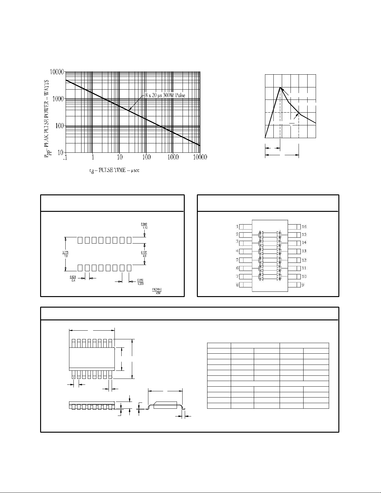
• Peak Pulse Power: 300 Watts (8/20 µsec, Figure 1) • Carrier tubes 50 pieces per (STANDARD)
• Pulse Repetition Rate: <.01%
ELECTRICAL CHARACTERISTICS@ 25
PART
NUMBER
SM16LC03C-6 MAL 3.3 4 7 9 200 25 -3
SM16LC05C-6 MAM 5.0 6 9.8 11 100 25 1
SM16LC12C-6 MAN 12 13.3 19 24 1 25 8
SM16LC15C-6 MAO 15 16.7 24 30 1 25 11
SM16LC24C-6 MAP 24 26.7 43 55 1 25 28
NOTE: Transient Voltage Suppression (TVS) product is normally selected based on its stand off voltage VWM. Product
selected voltage should be equal to or greater than the continuous peak operating voltage of the circuit to be protected.
Application: The SM16LCXXC-6 product is designed for transient voltage suppression protection of components at
the board level. It is an ideal product to be used for protection of I/O Transceivers.
DEVICE
MARKING
0
C to +1500C • 13 inch reel 2,500 pieces (OPTIONAL)
0
C Unless otherwise specified
STAND
OFF
VOLTAGE
V
WM
VOLTS
MAX MIN MAX MAX MAX TYP MAX
BREAKDOWN
VOLTAGE
V
BR
@1 mA
VOLTS
CLAMPING
VOLTAGE
V
C
@ 1 Amp
(FIGURE 2)
VOLTS
CLAMPING
VOLTAGE
V
C
@ 5 Amp
(FIGURE 2)
VOLTS
LEAKAGE
CURRENT
I
D
@ V
WM
µA
CAPACITANCE
(f=1 MHz)
@0V
C
pF
TEMPERATURE
COEFFICIENT
OF V
áV
mV/°C
BR
BR
MSC0979.PDF ISO 9001 CERTIFIED REV D 8/25/99

SM16LC03C-6 thru SM16LC24C-6
INCHES
MILLIMETERS
MAX
MIN
DIM
MAX
MIN
0.398 A0.358
9.09
10.10
0.158
0.150
3.81
4.01
0.069
0.053
1.35
1.75
0.021
0.011
0.28
0.53
0.050
0.016
0.41
1.27
0.050 BSC
1.27 BSC
0.010
0.006
0.15
0.25
0.008
0.004
0.10
0.20
0.206
0.189
4.80
5.23
B
C D F
G J K L0.244P0.228
5.79
6.19
WAVE FORMS
100
Peak Value -- Ipp
8 X 20 Waveform
50
Ipp
Half-Value --
0
0
Ipp -- Peak Pulse Current -- % Ipp
t
10
t
2
20 30
d
t -- Time in microsec
FIGURE 1 FIGURE 2
Peak Pulse Power Vs Pulse Time Pulse Wave Form
MOUNTING PAD SO-16 CIRCUIT DIAGRAM
SO-16 PACKAGE
A
B P
G
MSC0979.PDF ISO 9001 CERTIFIED REV D 8/25/99
D
J
C
K
L
F
 Loading...