Microsemi Corporation SG3546DM, SG3546LP Datasheet

LIN DOC #:
3546
SG3546
3.3V UNDERVOLTAGE SENSING CIRCUIT
THE INFINITE POWER OF INNOVATION
DESCRIPTION
The SG3546 is an undervoltage sensing
circuit specifically designed for use as
a reset controller in 3.3V
microprocessor-based applications. Its
micropower operation makes this
device ideal for portable applications
where extended battery life is required.
The device offers a 1.2V temperature
compensated bandgap reference, a
precision comparator with hysteresis
and a high-current open collector
output. This device operates from 1 to
10V input supply and drains <10µA in
the non-fault condition.
The SG3546 is available in an 8-pin
150mil SOIC package or a 3-pin TO-92
package and is rated for an ambient
temperature of 0°C to 70°C.
PRODUCT HIGHLIGHT
LOW-VOLTAGE MICROPROCESSOR RESET
2
1
POWER
SUPPLY
R
RESET
MICROPROCESSOR
C
DLY
P RODUCTION DAT A SHEET
KEY FEATURES
■ LOW STANDBY CURRENT
■ INTERNAL VOLTAGE THRESHOLD AT 2.95V
■ TEMPERATURE COMPENSATED BANDGAP
REFERENCE
■ PRECISION COMPARATOR WITH 40MV OF
HYSTERESIS
■ CLAMP DIODE FOR DISCHARGING DELAY
CAPACITOR
■ OUTPUT CURRENT SINK CAPABILITY
(typ 5mA)
■ 1-10V INPUT SUPPLY RANGE
■ AVAILABLE IN 150MIL, 8-PIN SOIC AND
3-PIN TO-92 PACKAGES
CIRCUIT
1.2 V
REF
3
PACKAGE ORDER INFORMATION
T
(°C)
A
Plastic SOIC
DM
8-pin
Plastic TO-92
LP
3-pin
0 to 70 SG3546DM SG3546LP
Note: All surface-mount packages are available in Tape & Reel.
Append the letter "T" to part number. (i.e. SG3546DMT)
Copyright © 1994
Rev. 1.3 1/96
FOR FURTHER INFORMATION CALL (714) 898-8121
11861 WESTERN AVENUE, GARDEN GROVE, CA. 92841
1

SG3546
PRODUCT DATABOOK 1996/1997
3.3V U
NDERVOLTAGE SENSING CIRCUIT
RODUCTION DATA SHEET
P
ABSOLUTE MAXIMUM RATINGS (Note 1)
Input Supply Voltage (VIN)............................................................................... -1V to 12V
RESET Output Voltage (V
Clamp Diode Forward Current .............................................................................. 100mA
) .......................................................................... -1V to 12V
OUT
Operating Junction Temperature
Plastic (DM - Package) ......................................................................................... 150°C
Storage Temperature Range...................................................................... -65°C to 150°C
Lead Temperature (Soldering, 10 seconds) ............................................................ 300°C
Note 1. Values beyond which damage may occur. All voltages are specified with respect to
ground, and all currents are positive into the specified terminal.
THERMAL DATA
DM PACKAGE:
THERMAL RESISTANCE-JUNCTION TO AMBIENT,
θθ
θ
θθ
JA
LP PACKAGE:
D
θθ
θ
θθ
x θ
JA
).
JA
THERMAL RESISTANCE-JUNCTION TO AMBIENT,
Junction Temperature Calculation: TJ = TA + (P
The θ
numbers are guidelines for the thermal performance of the device/pc-board system.
JA
All of the above assume no ambient airflow.
165°C/W
156°C/W
PACKAGE PIN OUTS
RESET
INPUT
N.C.
GROUND
1 8
2 7
3 6
4 5
DM PACKAGE
(Top View)
LP PACKAGE
(Top View)
N.C.
N.C.
N.C.
N.C.
3. GROUND
2. INPUT
1. RESET
INPUT
2
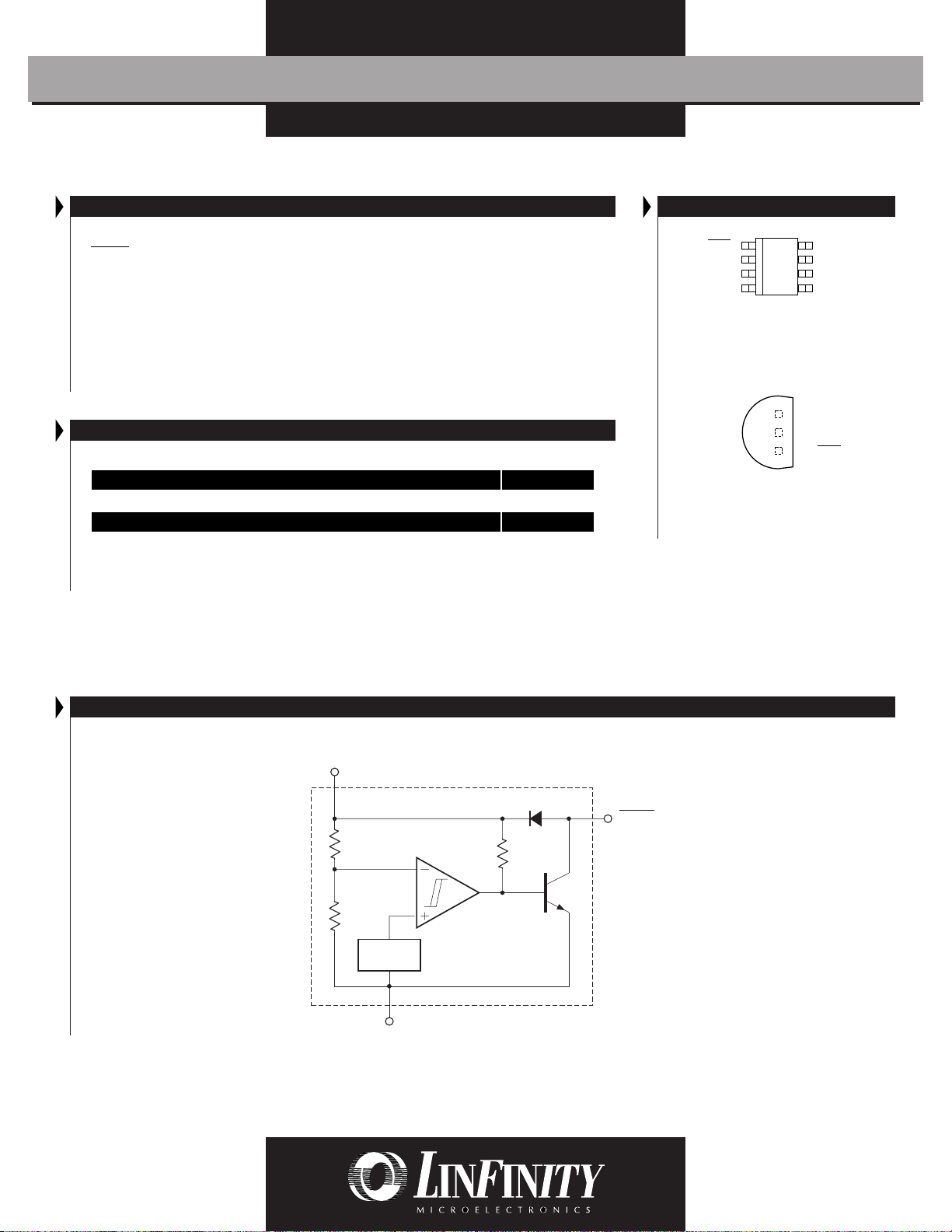
BLOCK DIAGRAM
1.2 V
REF
4
GROUND
RESET
1
2
Copyright © 1994
Rev. 1.3 2/96

PRODUCT DATABOOK 1996/1997
SG3546
3.3V UNDERVOLTAGE SENSING CIRCUIT
P RODUCTION DAT A SHEET
RECOMMENDED OPERATING CONDITIONS (Note 2)
Parameter
Input Supply Voltage
RESET Output Voltage
Clamp Diode Forward Current
Operating Ambient Temperature Range:
SG3546 T
Note 2. Range over which the device is guaranteed functional.
Symbol
A
ELECTRICAL CHARACTERISTICS
(Unless otherwise specified, these specifications apply over the operating ambient temperatures of 0°C ≤ TA ≤ 70°C for the SG3546. Low duty cycle
pulse testing techniques are used which maintains junction and case temperatures equal to the ambient temperature.)
Parameter
Symbol
Test Conditions Units
Total Device
Operating Input Voltage Range V
Quiescent Input Current I
IN
IN
VIN = 3.3V
= 10V
V
IN
Comparator Section
Threshold Voltage
High-State Output V
Low-State Output VILVIN Decreasing
Hysteresis V
IH
H
VIN Increasing
RESET Output Section
Output Sink Saturation V
Output Sink Current I
Output Off-State Leakage V
Clamp Diode Forward Voltage VFPin 1 to pin 2, (IF = 5.0mA)
OLVIN
SINKVIN
= 2.6V, I
= 1.0V, I
V
IN
, RESET = 2.6V
, RESET = 3.6V
IN
VIN , RESET = 10V
= 1mA
SINK
= 100µA
SINK
Recommended Operating Conditions
Min. Typ. Max.
110V
10 V
50 mA
070°C
Units
SG3546
Min. Typ. Max.
1.0 10 V
10 20 µA
19 50 µA
2.75 2.81 3.0 V
2.75 2.86 3.0 V
40 mV
0.05 0.40 V
0.06 0.30 V
20 mA
0.5 µA
2.0 µA
0.5 1.2 V
Copyright © 1994
Rev. 1.3 2/96
3
 Loading...