SG1540/SG2540/SG3540
OFF-LINE START-UP CONTROLLER
DESCRIPTION
The SG1540 is an integrated circuit designed to efficiently provide
start-up power from a high-voltage DC bus to a PWM control circuit
in a switching power supply. When used on the primary side, it
reduces start-up current to less than 1mA and allows any standard
PWM control circuit to be used as a primary-side controller. When
used to power a controller on the secondary side, it efficiently
eliminates the need for a heavy 50/60Hz line transformer with its
associated low frequency magnetic fields.
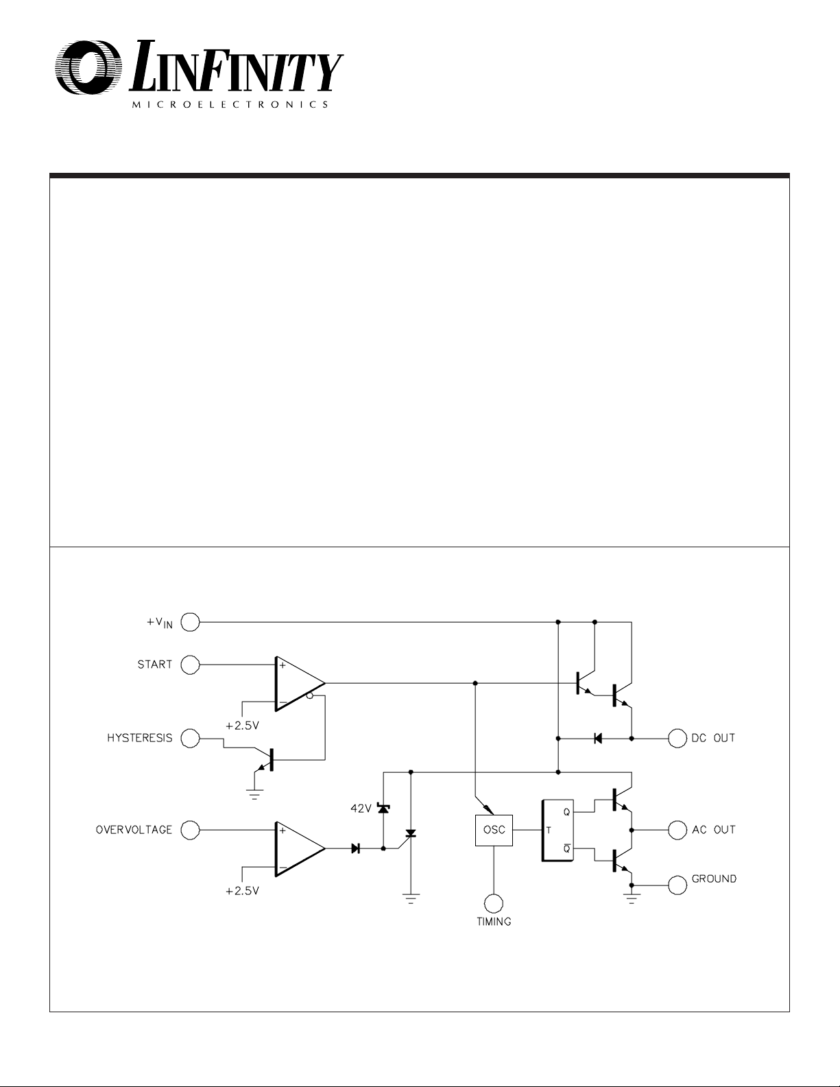
The circuit consists of three sections: a micropower bandgap
comparator/power switch referenced to 2.5 volts which isolates the
start-up capacitor from its load; a high frequency square-wave
oscillator with 200mA totem-pole output for driving an isolation
transformer; and a second bandgap comparator with latching
crowbar to protect against overvoltage faults while starting or
running.
The SG1540 is specified for operation over the full military ambient
temperature range of -55°C to 125°C. The SG2540 is characterized for the industrial range of -25°C to 85°C, and the SG3540 is
designed for the commercial range of 0°C to 70°C.
BLOCK DIAGRAM
FEATURES
••
• Useable with primary and secondary side PWM
••
controllers
••
• Micropower comparator / switch
••
- Internal 2.5V bandgap reference
- 50mA power switch
••
• Squarewave oscillator
••
- 500Hz to 200KHz operation
- 200mA totem pole outputs
••
• Eliminates bulky, expensive 50/60 Hz transformer
••
••
• Minimizes high voltage bleeder current
••
••
• Programmable start-up voltage and hysteresis
••
••
• Internal and programmable overvoltage crowbar
••
latch
••
• Available in 8 pin DIP, 10 pin flat pack, and 16 pin
••
widebody SOIC
HIGH RELIABILITY FEATURES - SG1540
♦♦
♦ Available to MIL-STD - 883
♦♦
♦♦
♦ LMI level "S" processing available
♦♦
4/90 Rev 1.1 2/94 LINFINITY Microelectronics Inc.
Copyright 1994 11861 Western Avenue
1 (714) 898-8121
∞ ∞
∞ Garden Grove, CA 92841
∞ ∞
∞∞
∞ FAX: (714) 893-2570
∞∞

ABSOLUTE MAXIMUM RATINGS (Note 1)
Supply Voltage (+V
DC Output Current, Continuous (V
AC Output Current, Continuous ..................................... 200mA
Analog Inputs (Start and Overvoltage) .................-0.3V to 6.0V
Analog Input Currents (V>8V).......................................... 10mA
Overvoltage Crowbar Current, Continuous ..................... 50mA
Note 1. Values beyond which damage may occur.
)........................................................ +37V
IN
)........................... 100mA
OUT
THERMAL DATA
Y Package:
Thermal ResistanceThermal Resistance-
M Package:
Thermal ResistanceThermal Resistance-
DW Package:
Thermal ResistanceThermal Resistance-
Junction to Case, θ
Junction to Ambient, θ
Junction to Case, θ
Junction to Ambient, θ
Junction to Case, θ
Junction to Ambient, θ
JC
JC
JC
.................. 50°C/W
............ 130°C/W
JA
.................. 60°C/W
............. 95°C/W
JA
.................. 40°C/W
............. 95°C/W
JA
RECOMMENDED OPERATING CONDITIONS (Note 2)
Supply Voltage Range ............................................... 7V to 35V
DC Output Current, Continuous................................ 0 to 50mA
AC Output Current, Continuous ............................. 0 to 100 mA
Oscillator Frequency Range ........................... 1KHz to 400KHz
Timing Resistor Range ...................................... 2KΩ to 150KΩ
Note 2. Range over which the device is functional.
SG1540/SG2540/SG3540
Overvoltage Crowbar Energy (½CV²)................................. 8mJ
Operating Junction Temperature
Hermetic (Y Package) ................................................ 150°C
Plastic (M, DW Packages) .......................................... 150°C
Storage Temperature Range ............................ -65°C to 150°C
Lead Temperature (Soldering, 10 Seconds) .................. 300°C
Note A. Junction Temperature Calculation: TJ = TA + (PD x θJA).
Note B. The above numbers for θ
thermal resistance of the package in a standard mounting configuration. The θ
guidelines for the thermal performance of the device/pcboard system. All of the above assume no ambient
airflow.
Timing Capacitor Range ........................................ 1nF to 20µF
Operating Ambient Temperature Range
SG1540 ...........................................................-55°C to 125°C
SG2540 .............................................................-25°C to 85°C
SG3540 ................................................................ 0°C to 70°C
are maximums for the limiting
JC
numbers are meant to be
JA
ELECTRICAL CHARACTERISTICS
(Unless otherwise specified, these specifications apply over the operating ambient temperatures for SG1540 with -55°C ≤ TA ≤ 125°C, SG2540 with
-25°C ≤ TA ≤ 85°C, SG3540 with 0°C ≤ TA ≤ 70°C, and +VIN = 15V. A 0.1µF high frequency bypass capacitor is recommended on VIN. Low duty cycle
testing techniques are used which maintains junction and case temperatures equal to the ambient temperature.)
SG1540/2540/3540
Min.
Typ. Max.
0.2
0.4
0.3
0.6
3
6
2.37
2.50
2.63
6
12.5
12.0
50
0.1
0.1
13.5
13.0
100 225
1
7
8
0.2
Units
mA
mA
mA
V
µA
V
V
V
V
mA
Start-up Section
Start Current I
CC
Operating Current
Start Threshold
Start Bias Current
Start Clamp Voltage
Hysteresis ON Voltage
DC Output Section
Voltage
V
OUT
Short Circuit Current
V
= 0 to 2.37V
START
V
TIMING
F
= 50KHz, V
OSC
= 0 to 5V
V
PIN 1
I
= 1mA
PIN 1
= 100µA
I
PIN 4
I
SOURCE
I
SOURCE
V
= 0V
OUT
= +VIN; V
= 10mA
= 50mA
Test ConditionsParameter
Open
OUT
and AC
OUT
OUT
Open
4/90 Rev 1.1 2/94 LINFINITY Microelectronics Inc.
Copyright 1994 11861 Western Avenue
2 (714) 898-8121
∞ ∞
∞ Garden Grove, CA 92841
∞ ∞
∞∞
∞ FAX: (714) 893-2570
∞∞
 Loading...