SG1524/SG2524/SG3524
4/90 Rev 1.1 2/94 LINFINITY Microelectronics Inc.
Copyright 1994 11861 Western Avenue
∞ ∞
∞ ∞
∞ Garden Grove, CA 92841
1 (714) 898-8121
∞∞
∞∞
∞ FAX: (714) 893-2570
REGULATING PULSE WIDTH MODULATOR
FEATURES
••
••
• 8V to 40V operation
••
••
• 5V reference
••
••
• Reference line and load regulation of 0.4%
••
••
• Reference temperature coefficient < ± 1%
••
••
• 100Hz to 300KHz oscillator range
••
••
• Excellent external sync capability
••
••
• Dual 50mA output transistors
••
••
• Current limit circuitry
••
••
• Complete PWM power control circuitry
••
••
• Single ended or push-pull outputs
••
••
• Total supply current less than 10mA
HIGH RELIABILITY FEATURES - SG1524
♦♦
♦♦
♦ Available to MIL-STD-883B and DESC SMD
♦♦
♦♦
♦ MIL-M-38510/12601BEA - JAN1524J
♦♦
♦♦
♦ Radiation data available
♦♦
♦♦
♦ LMI level "S" processing available
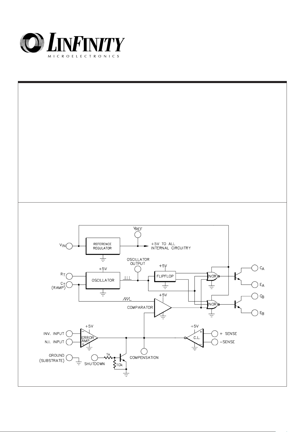
BLOCK DIAGRAM
DESCRIPTION
This monolithic integrated circuit contains all the control circuitry for a
regulating power supply inverter or switching regulator. Included in a 16pin dual-in-line package is the voltage reference, error amplifier, oscillator,
pulse width modulator, pulse steering flip-flop, dual alternating output
switches and current limiting and shut-down circuitry. This device can be
used for switching regulators of either polarity, transformer coupled DC to
DC converters, transformerless voltage doublers and polarity converters,
as well as other power applications. The SG1524 is specified for operation
over the full military ambient temperature range of -55°C to +125°C, the
SG2524 for -25°C to +85°C, and the SG3524 is designed for commercial
applications of 0°C to +70°C.

SG1524/SG2524/SG3524
4/90 Rev 1.1 2/94 LINFINITY Microelectronics Inc.
Copyright 1994 11861 Western Avenue
∞ ∞
∞ ∞
∞ Garden Grove, CA 92841
2 (714) 898-8121
∞∞
∞∞
∞ FAX: (714) 893-2570
Oscillator Charging Current ................................................5mA
Operating Junction Temperature
Hermetic (J, L Packages) .............................................150°C
Plastic (N, D Packages) ............................................... 150°C
Storage Temperature Range .............................-65°C to 150°C
Lead Temperature (Soldering, 10 seconds) ....................300°C
Input Voltage (+VIN)............................................................. 42V
Collector Voltage ................................................................ 40V
Logic Inputs...........................................................-0.3V to 5.5V
Current Limit Sense Inputs ...................................-0.3V to 0.3V
Output Current (each transistor) .................................... 100mA
Reference Load Current .................................................. 50mA
ABSOLUTE MAXIMUM RATINGS (Note 1)
Note 1. Values beyond which damage may occur.
Input Voltage (+VIN) ...................................................
Collector Voltage .......................................................
Error Amp Common Mode Range ..........................
Current Limit Sense Common Mode Range ........
Output Current (each transistor) ...............................
Reference Load Current ...........................................
Oscillator Charging Current ..................................
8V to 40V
0V to 40V
1.8V to 3.4V
-0.3V to 0.3V
0 to 50mA
0 to 20mA
30µA to 2mA
Oscillator Frequency Range .........................
Oscillator Timing Resistor (R
T
) ........................
Oscillator Timing Capacitor (C
T
) ............................
Operating Ambient Temperature Range
SG1524 .........................................................
SG2524 ...........................................................
SG3524 ...............................................................
100Hz to 300KHz
1.8KΩ to 100KΩ
1nF to 1.0µF
-55°C to 125°C
-25°C to 85°C
0°C to 70°C
Note 2: Range over which the device is functional and parameter limits are guaranteed.
RECOMMENDED OPERATING CONDITIONS (Note 2)
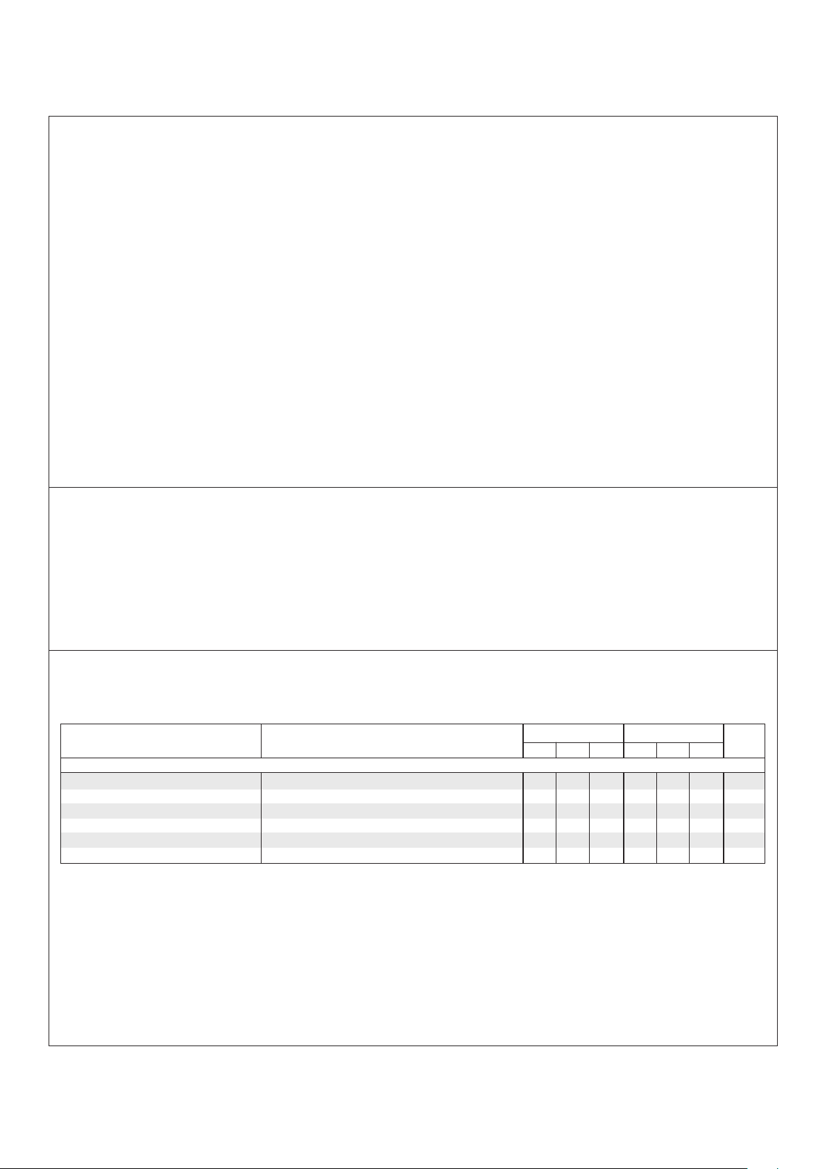
ELECTRICAL CHARACTERISTICS
(Unless otherwise specified, these specifications apply over the operating ambient temperatures for SG1524 with -55° C ≤ TA ≤ 125°C, SG2524 with
-25°C ≤ T
A
≤ 85°C, SG3524 with 0°C ≤ TA ≤ 70°C, and +VIN = 20V. Low duty cycle pulse testing techniques are used which maintains junction and
case temperatures equal to the ambient temperature.)
Note 3. I
L
= 0mA
5.00
50
Reference Section
(Note 3)
TJ = 25°C
V
IN
= 8V to 40V
I
L
= 0 to 20mA
Over Operating Temperature Range
Over Line, Load and Temperature
V
REF
= 0V
Output Voltage
Line Regulation
Load Regulation
Temperature Stability
(Note 7)
Total Output Voltage Range (Note 7)
Short Circuit Current
Min. Typ. Max.
Min. Typ. Max.
SG3524SG1524/2524
UnitsTest ConditionsParameter
4.80
4.80
25
5.20
20
50
50
5.20
150
4.60
4.60
25
5.00505.40
30
50
50
5.40
150
V
mV
mV
mV
V
mA
THERMAL DATA
J Package:
Thermal Resistance-
Junction to Case, θ
JC
.................. 30°C/W
Thermal Resistance-
Junction to Ambient, θ
JA
.............. 80°C/W
N Package:
Thermal Resistance-
Junction to Case, θ
JC
.................. 40°C/W
Thermal Resistance-
Junction to Ambient, θ
JA
............. 65°C/W
D Package:
Thermal Resistance-
Junction to Case, θ
JC
................... 50°C/W
Thermal Resistance-
Junction to Ambient, θ
JA
............ 120°C/W
L Package:
Thermal Resistance-
Junction to Case, θ
JC
.................. 35°C/W
Thermal Resistance-
Junction to Ambient, θ
JA
........... 120°C/W
Note A. Junction Temperature Calculation: TJ = TA + (PD x θJA).
Note B. The above numbers for
θJC are maximums for the limiting
thermal resistance of the package in a standard mounting configuration. The θ
JA
numbers are meant to be
guidelines for the thermal performance of the device/pcboard system. All of the above assume no ambient
airflow.
 Loading...