Microsemi Corporation SG2804L, SG2811J, SG2811L, SG2812J, SG2812L Datasheet

SG2800 SERIES
4/90 Rev 1.5 11/97 LINFINITY Microelectronics Inc.
Copyright 1997 11861 Western Avenue
∞ ∞
∞ ∞
∞ Garden Grove, CA 92841
1 (714) 898-8121
∞∞
∞∞
∞ FAX: (714) 893-2570
DESCRIPTION
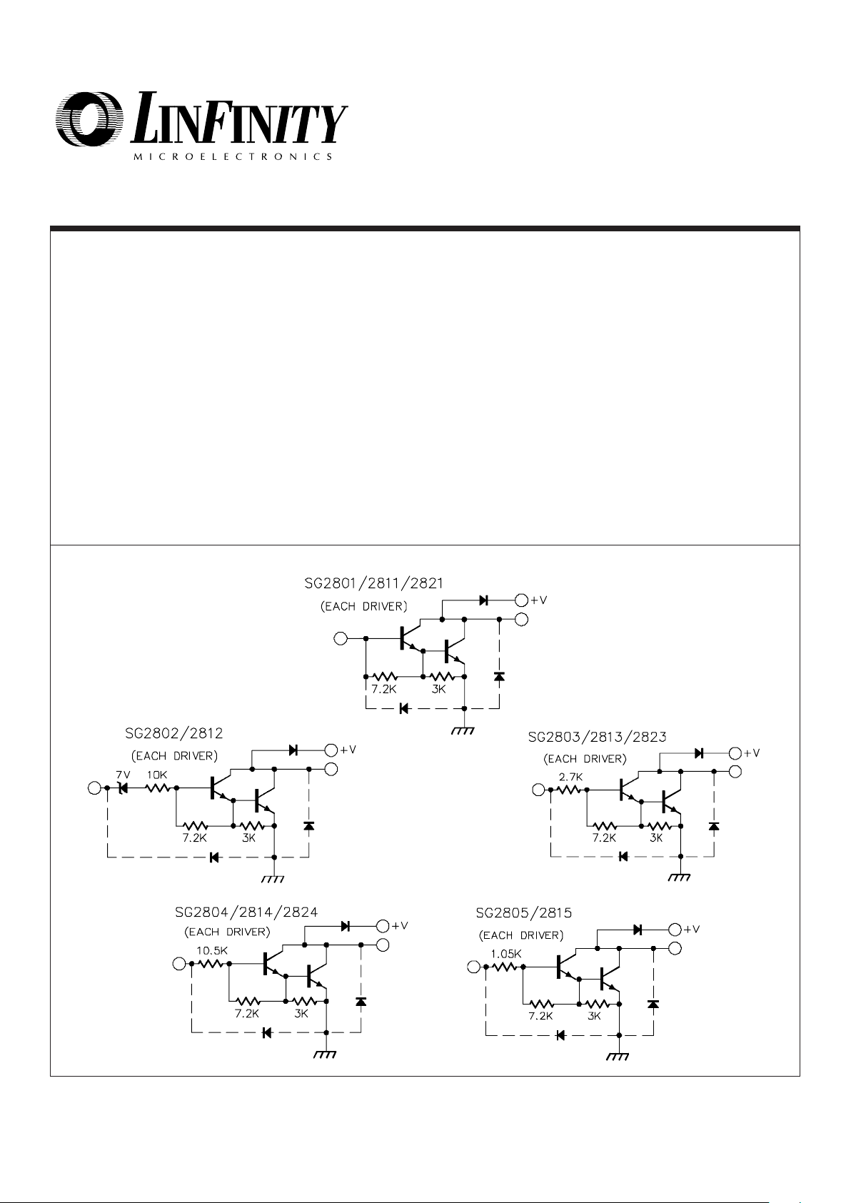
The SG2800 series integrates eight NPN Darlington pairs with
internal suppression diodes to drive lamps, relays, and solenoids in
many military, aerospace, and industrial applications that require
severe environments. All units feature open collector outputs with
greater than 50V breakdown voltages combined with 500mA
current carrying capabilities. Five different input configurations
provide optimized designs for interfacing with DTL, TTL, PMOS, or
CMOS drive signals. These devices are designed to operate from
-55°C to 125°C ambient temperature in a 18-pin dual in-line
ceramic (J) package and 20-pin leadless chip carrier (LCC).
FEATURES
••
••
• Eight NPN Darlington pairs
••
••
• Collector currents to 600mA
••
••
• Output voltages from 50V to 95V
••
••
• Internal clamping diodes for inductive loads
••
••
• DTL, TTL, PMOS, or CMOS compatible inputs
••
••
• Hermetic ceramic package
HIGH RELIABILITY FEATURES
♦♦
♦♦
♦ Available to MIL-STD-883 and DESC SMD
♦♦
♦♦
♦ MIL-M38510/14106BVA - JAN2801J
♦♦
♦♦
♦ MIL-M38510/14107BVA - JAN2802J
♦♦
♦♦
♦ MIL-M38510/14108BVA - JAN2803J
♦♦
♦♦
♦ MIL-M38510/14109BVA - JAN2804J
♦♦
♦♦
♦ Radiation data available
♦♦
♦♦
♦ LMI level "S" processing available
HIGH VOL TA GE MEDIUM
CURRENT DRIVER ARRAYS
PARTIAL SCHEMATICS

SG2800 SERIES
4/90 Rev 1.5 11/97 LINFINITY Microelectronics Inc.
Copyright 1997 11861 Western Avenue
∞ ∞
∞ ∞
∞ Garden Grove, CA 92841
2 (714) 898-8121
∞∞
∞∞
∞ FAX: (714) 893-2570
ABSOLUTE MAXIMUM RATINGS (Note 1)
Continuous Collector Current, I
C
(SG2800, 2820) ......................................................
(SG2810) ...............................................................
Operating Junction Temperature
Hermetic (J, L Packages) .........................................
Plastic (N Package) ..................................................
Storage Temperature Range ..........................
Lead Temperature (Soldering 10 sec.) .........................
Output Voltage, V
CE
(SG2800, 2810 series) ................................................
(SG2820 series) ..........................................................
Input Voltage, V
IN
(SG2802,3,4 series) ....................................................
Continuous Input Current, I
IN
........................................
50V
95V
30V
25mA
500mA
600mA
150°C
150°C
-65°C to 150°C
300°C
Note 1. Values beyond which damage may occur.
J Package:
Thermal Resistance-
Junction to Case, θ
JC
.................. 25°C/W
Thermal Resistance-
Junction to Ambient, θ
JA
............... 70°C/W
N Package:
Thermal Resistance-
Junction to Case, θ
JC
.................. 30°C/W
Thermal Resistance-
Junction to Ambient, θ
JA
.............. 60°C/W
L Package:
Thermal Resistance-
Junction to Case, θ
JC
.................. 35°C/W
Thermal Resistance-
Junction to Ambient, θ
JA
............. 120°C/W
THERMAL DATA
Note A. Junction Temperature Calculation: TJ = TA + (PD x θJA).
Note B. The above numbers for
θJC are maximums for the limiting
thermal resistance of the package in a standard mounting configuration. The θ
JA
numbers are meant to be
guidelines for the thermal performance of the device/pcboard system. All of the above assume no ambient
airflow.
Output Voltage, V
CE
SG2800, SG2820 series ..............................................
SG2810 series .............................................................
50V
95V
Peak Collector Current, I
C
SG2800, SG2820 series .........................................
SG2810 series ........................................................
Operating Ambient Temperature Range ........
350mA
500mA
-55°C to 125°C
Note 2. Range over which the device is functional.
RECOMMENDED OPERATING CONDITIONS (Note 2)
SELECTION GUIDE
Device VCE Max IC Max Logic Inputs
SG2801 50V 500mA General Purpose
PMOS, CMOS
SG2802 50V 500mA 14V-25V PMOS
SG2803 50V 500mA 5V TTL, CMOS
SG2804 50V 500mA 6V-15V CMOS, PMOS
SG2811 50V 600mA General Purpose
PMOS, CMOS
SG2812 50V 600mA 14V-25V PMOS
Device VCE Max IC Max Logic Inputs
SG2813 50V 600mA 5V TTL, CMOS
SG2814 50V 600mA 6V-15V CMOS, PMOS
SG2815 50V 600mA High Output TTL
SG2821 95V 500mA General Purpose
PMOS, CMOS
SG2823 95V 500mA 5V TTL, CMOS
SG2824 95V 500mA 6V-15V CMOS, PMOS

SG2800 SERIES
4/90 Rev 1.5 11/97 LINFINITY Microelectronics Inc.
Copyright 1997 11861 Western Avenue
∞ ∞
∞ ∞
∞ Garden Grove, CA 92841
3 (714) 898-8121
∞∞
∞∞
∞ FAX: (714) 893-2570
ELECTRICAL CHARACTERISTICS
(Unless otherwise specified, these specifications apply over the operating ambient temperatures of -55°C ≤ TA ≤ 125°C. Low duty cycle pulse testing
techniques are used which maintains junction and case temperatures equal to the ambient temperature.)
Parameter Units
Min. Typ. Max.
Limits
Test Conditions
Applicable
Devices
Temp.
SG2801 thru SG2804
All
SG2802
SG2804
All
SG2802
SG2803
SG2804
All
SG2802
SG2803
SG2804
SG2801
All
All
All
All
All
Output Leakage Current (I
CEX
)
Collector - Emitter (V
CE(SAT)
)
Input Current (I
IN(ON)
)
(I
IN(OFF)
)
Input Voltage (V
IN(ON)
)
D-C Forward Current
Transfer Ratio (h
FE
)
Input Capacitance (C
IN
) (Note 3)
Turn-On Delay (TPLH)
Turn-Off Delay (TPHL)
Clamp Diode Leakage Current (I
R
)
Clamp Diode Forward Voltage (V
F
)
T
A
= T
MIN
TA = T
MIN
TA = T
MIN
TA = 25°C
T
A
= 25°C
T
A
= 25°C
T
A
= T
MAX
TA = T
MAX
TA = T
MAX
TA = T
MAX
TA = T
MIN
TA = T
MAX
TA = T
MIN
TA = T
MIN
TA = T
MIN
TA = T
MAX
TA = T
MAX
TA = T
MAX
TA = T
MIN
TA = T
MIN
TA = T
MIN
TA = T
MIN
TA = T
MAX
TA = T
MAX
TA = T
MAX
TA = T
MAX
TA = T
MIN
TA = 25°C
T
A
= 25°C
T
A
= 25°C
T
A
= 25°C
V
CE
= 50V
V
CE
= 50V, VIN = 6V
V
CE
= 50V, VIN = 1V
I
C
= 350mA, IB = 850µA
I
C
= 200mA, IB = 550µA
I
C
= 100mA, IB = 350µA
I
C
= 350mA, IB = 500µA
I
C
= 200mA, IB = 350µA
I
C
= 100mA, IB = 250µA
I
C
= 350mA, IB = 500µA
I
C
= 200mA, IB = 350µA
I
C
= 100mA, IB = 250µA
V
IN
= 17V
V
IN
= 3.85V
V
IN
= 5V
V
IN
= 12V
I
C
= 500µA
V
CE
= 2V, IC = 300mA
V
CE
= 2V, IC = 300mA
V
CE
= 2V, IC = 200mA
V
CE
= 2V, IC = 250mA
V
CE
= 2V, IC = 300mA
V
CE
= 2V, IC = 200mA
V
CE
= 2V, IC = 250mA
V
CE
= 2V, IC = 300mA
V
CE
= 2V, IC = 125mA
V
CE
= 2V, IC = 200mA
V
CE
= 2V, IC = 275mA
V
CE
= 2V, IC = 350mA
V
CE
= 2V, IC = 125mA
V
CE
= 2V, IC = 200mA
V
CE
= 2V, IC = 275mA
V
CE
= 2V, IC = 350mA
V
CE
= 2V, IC = 350mA
V
CE
= 2V, IC = 350mA
0.5 E
IN
to 0.5 E
OUT
0.5 EIN to 0.5 E
OUT
VR = 50V
I
F
= 350mA
100
500
500
1.8
1.5
1.3
1.6
1.3
1.1
1.8
1.5
1.3
1300
1350
500
1450
18
13
3.3
3.6
3.9
2.4
2.7
3.0
6.0
8.0
10
12
5.0
6.0
7.0
8.0
25
1000
1000
50
2.0
480
650
240
650
25
500
1000
1.6
1.3
1.1
1.25
1.1
0.9
1.6
1.3
1.1
850
930
350
1000
50
15
250
250
1.7
µA
µA
µA
V
V
V
V
V
V
V
V
V
µA
µA
µA
µA
µA
V
V
V
V
V
V
V
V
V
V
V
V
V
V
V
V
pF
ns
ns
µA
V
Note 3. These parameters, although guaranteed, are not tested in production.
 Loading...