

Page 1

User Guide
SA.45s Chip-Scale Atomic Clock
Page 2

SA.45s Chip-Scale Atomic Clock
Contents
1 Revision History ............................................................................................................................. 1
1.1 Revision D ........................................................................................................................................... 1
1.2 Revision C ........................................................................................................................................... 1
1.3 Revision B ........................................................................................................................................... 1
1.4 Revision A ........................................................................................................................................... 1
2 Preface ........................................................................................................................................... 2
2.1 About This Document ......................................................................................................................... 2
2.2 Intended Audience ............................................................................................................................. 2
2.3 Warnings, Cautions, Recommendations, and Notes .......................................................................... 2
2.4 Reference Documents ........................................................................................................................ 2
3 SA.45s Chip-Scale Atomic Clock ..................................................................................................... 3
3.1 Introduction ........................................................................................................................................ 3
3.2 SA.45s Overview ................................................................................................................................. 3
3.2.1 Precautions .............................................................................................................................................. 3
3.2.2 Packaging ................................................................................................................................................. 4
3.2.3 Absolute Minimum and Maximum Ratings ............................................................................................. 4
3.2.4 Mechanical Interface and Mounting Considerations .............................................................................. 4
3.2.5 Recommended Operating Characteristics ............................................................................................... 5
3.3 Functional Description ........................................................................................................................ 6
3.3.1 Principle of Operation ............................................................................................................................. 6
3.3.2 Start-Up Sequence .................................................................................................................................. 7
3.3.3 Built-In Test Equipment (BITE) ................................................................................................................ 7
3.3.4 RF Output Characteristics ........................................................................................................................ 7
3.3.5 What to Expect During First Power-Up ................................................................................................... 8
3.3.6 Frequency Steering .................................................................................................................................. 8
3.3.7 1PPS Output .......................................................................................................................................... 10
3.3.8 1PPS Synchronization ............................................................................................................................ 10
3.3.9 1PPS Disciplining ................................................................................................................................... 12
3.3.10 Time-of-Day ......................................................................................................................................... 13
3.3.11 Analog Tuning ...................................................................................................................................... 14
3.3.12 Ultra-Low Power Operating Mode ...................................................................................................... 15
3.3.13 1PPS Phase Measurement Mode ........................................................................................................ 17
3.4 Programmers Reference ................................................................................................................... 17
3.4.1 Overview of Telemetry Interface .......................................................................................................... 17
3.4.2 Command Summary .............................................................................................................................. 19
3.4.3 Detailed Command Descriptions ........................................................................................................... 20
3.5 Developer's Kit .................................................................................................................................. 29
SA.45s CSAC User Guide Revision D
Page 3

SA.45s Chip-Scale Atomic Clock
3.5.1 Package Contents .................................................................................................................................. 29
3.5.2 Evaluation Board Overview ................................................................................................................... 29
3.5.3 Installing the CSAC on the Test Fixture ................................................................................................. 31
3.5.4 Cabling ................................................................................................................................................... 31
3.5.5 CSACdemo Software Installation ........................................................................................................... 31
3.5.6 CSACdemo Operation ............................................................................................................................ 31
3.6 Data Acquisition with CSACdemo ..................................................................................................... 34
3.7 Design Guide ..................................................................................................................................... 35
3.7.1 The Art of Disciplining ........................................................................................................................... 35
3.7.2 Heat Sink ............................................................................................................................................... 37
3.7.3 Notes on Soldering ................................................................................................................................ 37
3.7.4 Notes on the Evaluation Board ............................................................................................................. 37
3.7.5 Time Error of a CSAC ............................................................................................................................. 38
3.7.6 Writes to NVRAM .................................................................................................................................. 39
SA.45s CSAC User Guide Revision D
Page 4

SA.45s Chip-Scale Atomic Clock
1 Revision History
The revision history describes the changes that were implemented in the document. The changes are
listed by revision, starting with the most current publication.
1.1 Revision D
Revision D was published in August 2017. It was updated to clarify frequency steering and other edits
per EC12643.
1.2 Revision C
Revision C was published in July 2016. It was updated to reflect 1.08 and 1.09 firmware implementation
as per EC11049.
1.3 Revision B
Revision B was published May 2014. It was updated to reflect 1.06 and 1.07 firmware implementation
and Microsemi branding as per EC09876.
1.4 Revision A
Revision A was published in July 2011. It was the first publication of this document.
SA.45s CSAC User Guide Revision D 1
Page 5

SA.45s Chip-Scale Atomic Clock
2 Preface
2.1 About This Document
The SA.45s user guide provides basic recommendations for designing products to use Microsemi's
SA.45s Chip-Scale Atomic Clock (CSAC). The guidelines in the document are generic because specific
product requirements vary from one application to the other.
This material consists of a brief description of SA.45s design supported by block diagrams, description of
environmental issues, installation guidelines, and unit operation.
2.2 Intended Audience
This document is intended for engineers and telecommunications professionals who are designing,
installing, operating, or maintaining time, frequency, and synchronization systems having a requirement
for a low profile and highly precise frequency generator.
To use this document effectively, you should have a good understanding of digital telecommunications
technologies and analog frequency generation and synthesis techniques.
2.3 Warnings, Cautions, Recommendations, and Notes
Warning: To avoid serious personal injury or death, do not disregard warnings. All warnings use this
symbol. Warnings are installation, operation, or maintenance procedures, practices, or statements, that
if not strictly observed, may result in serious personal injury or even death.
Caution: To avoid personal injury, do not disregard cautions. All cautions use this symbol. Cautions are
installation, operation, or maintenance procedures, practices, conditions, or statements, that if not
strictly observed, may result in damage to, or destruction of, the equipment. Cautions are also used to
indicate a long-term health hazard.
ESD Caution: To avoid personal injury and electrostatic discharge (ESD) damage to equipment, do not
disregard ESD cautions. All ESD cautions use this symbol. ESD cautions are installation, operation, or
maintenance procedures, practices, conditions, or statements that if not strictly observed, may result in
possible personal injury, electrostatic discharge damage to, or destruction of, static-sensitive
components of the equipment.
Note: All notes use this symbol. Notes contain installation, operation, or maintenance procedures,
practices, conditions, or statements that alert you to important information, which may make your task
easier or increase your understanding.
Note: Microsemi offers training courses designed to enhance your knowledge of the SA.45s Cesium
Frequency Standard. Contact your local representative or sales office for a complete list of courses and
outlines.
2.4 Reference Documents
For additional information about the products described in this guide, please contact your Microsemi
representative or your local sales office. You can also contact us on the web at .www.microsemi.com
CSAC Developer's Kit (990-00123-000)
CSACdemo Software (084-00365-000)
SA.45s CSAC User Guide Revision D 2
Page 6
SA.45s Chip-Scale Atomic Clock
3 SA.45s Chip-Scale Atomic Clock
3.1 Introduction
The Microsemi Quantum™ Model SA.45s Chip-Scale Atomic Clock (CSAC) is the world's smallest, lowest
power atomic clock technology. This user's reference guide provides the basic guidelines and
recommendations for designing products with the SA.45s reference. These are generic, and should be
tailored for each application.
This document is intended for engineers, technicians, and technologists who are designing, installing,
operating or maintaining time, frequency, and synchronization systems. The SA.45s is a low profile,
highly precise frequency generator. To use this document effectively, an understanding of digital
communication technologies is required. It is advantageous to have a background in frequency
generation and synthesis techniques.
3.2 SA.45s Overview
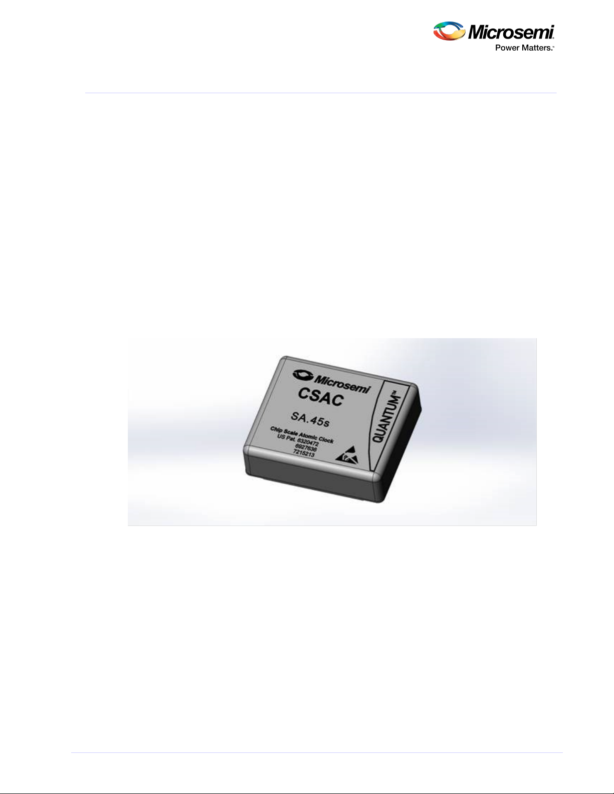
The Microsemi SA.45s CSAC is the world's first commercially available chip-scale atomic clock, providing
the accuracy and stability of atomic clock technology while achieving true breakthroughs in reduced
size, weight, and power consumption. The small size (less than 17 cc) and low power consumption of the
CSAC (less than 125 mW) enables atomic timing accuracy in portable, battery-powered applications.
Figure 1 • Microsemi Quantum SA.45s Chip-Scale Atomic Clock (CSAC)
The SA.45s provides RF and 1PPS outputs at standard CMOS levels. It accepts a 1PPS input to
synchronize the output to within 100 ns of a reference clock. It can also discipline its phase and
frequency to within 1 ns and 1 × 10 , respectively.
–12
This user guide provides engineering information for use of the SA.45s. It also provides supporting
information for use of the developer's kit (p/n 990-00123-00x). Furthermore, the design details of the
developer's kit can be used to assist with host system design (for example, power conditioning or signal
buffering). This guide must be used in conjunction with the current datasheet for SA.45s, which is
available on the Microsemi web site at www.microsemi.com.
3.2.1 Precautions
ESD Caution: To avoid electrostatic discharge (ESD) damage, proper ESD handling procedures must be
observed in unpacking, assembling, and testing the CSAC.
SA.45s CSAC User Guide Revision D 3
Page 7
SA.45s Chip-Scale Atomic Clock
3.2.2 Packaging
Retain the original CSAC ESD-safe packaging material in the event that the device needs to be returned
to Microsemi for service.
3.2.3 Absolute Minimum and Maximum Ratings
The following table indicates the absolute minimum and maximum ratings to which the CSAC can be
subjected without permanent unrecoverable damage.
The CSAC cannot be expected to perform normally when operated outside of the recommended Note:
operating conditions. All ratings apply at 25°C, unless otherwise noted.
Table 1 • Absolute Maximum Ratings
Parameter Rating
Supply voltage (V )CC 0 V–4.1 V
Analog tuning voltage 0 V–VCC
Maximum current draw 1PPS input, RS232, BITE: ±2 mA
1PPS output, RF output: ±20 mA
Storage temperature –55 °C to 85 °C
Refer to the Note: SA.45s datasheet for updated parameters.
3.2.4 Mechanical Interface and Mounting Considerations
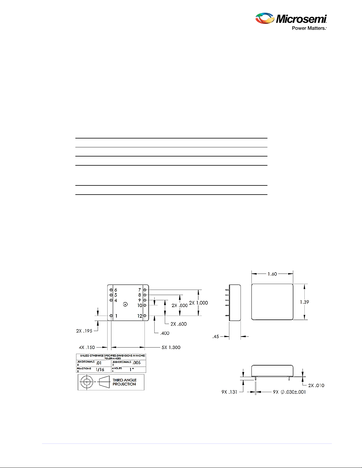
The physical dimensions of the SA.45s CSAC are 1.6" x 1.4" x 0.45" H. The following illustration shows
the detailed dimensions of CSAC. The CSAC baseplate and cover are 80% nickel-iron magnetic alloy per
ASTM A753, Type 4 (Mu-Metal or Hy-Mu80™).
Figure 2 • CSAC Mechanical Drawing
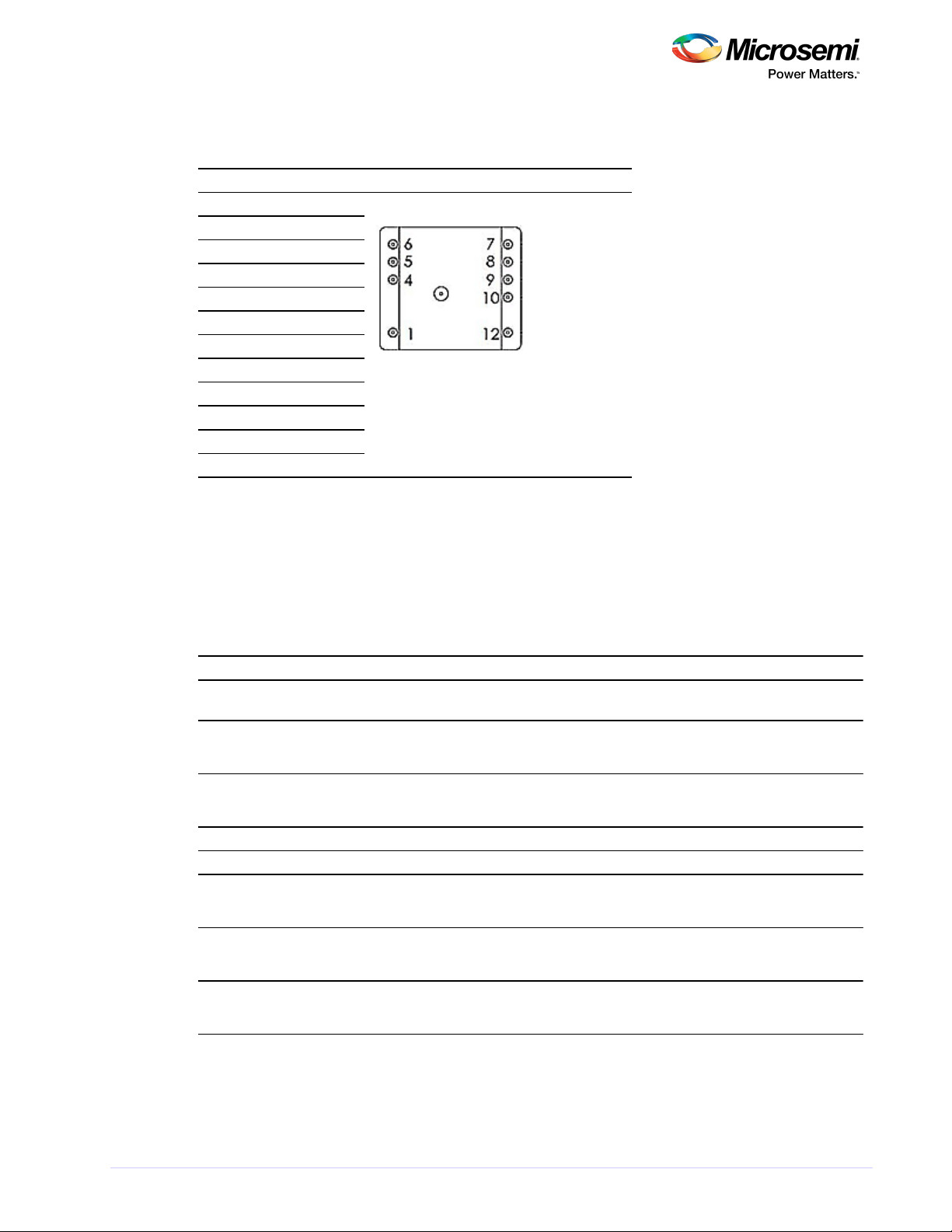
following table The shows the pinout of the SA.45s CSAC.
SA.45s CSAC User Guide Revision D 4
Page 8
SA.45s Chip-Scale Atomic Clock
Table 2 • SA45s CSAC Pinout
PIN I.D.
1 Tune
Bottom view
2 N/A
3 N/A
4 BITE
5 Tx
6 Rx
7 VCC
8 GND
9 1PPS input
10 1PPS output
11 N/A
12 RF output
Note: Pins labeled N/A are not present in the SA.45s.
3.2.5 Recommended Operating Characteristics
The SA.45 pinout is shown in the previous table . The electrical function of each pin is shown in the
following table.
Table 3 • Recommended Operating Characteristics
PIN Function Level Reference Section
1 Analog tuning input10 V–2.5 V "Analog Tuning" section (see page
14)
4 Built-in test
equipment (BITE)
2
LogicH > 2.8 V
LogicL < 0.3 V
"Built-In Test Equipment (BITE)"
section (see page 7)
5, 6 RS232 2.8 V < LogicH < VCC
0 V < LogicL < 0.3 V
"Programmers Reference" section
(see page 17)
7 VCC 3.3 VDC ± 0.1 VDC
8 Ground
9 1PPS in
3
2.5 V < LogicH < VCC
0 V < LogicL < 0.5 V
10 1PPS out
4, 5
2.8 V < LogicH < VCC
0 V < LogicL < 0.3 V
"1PPS Output" section (see page
10)
12 RF out 2.8 V < LogicH < VCC
0 V < LogicL < 0.3 V
"RF Output Characteristics" section
(see page 7)
SA.45s CSAC User Guide Revision D 5
Page 9
SA.45s Chip-Scale Atomic Clock
1.
2.
3.
4.
5.
6.
Notes:
Analog Tuning Sensitivity is Δf/f = (V – 1250 mV) × 1.77 × 10 /mVtune
–11
Built-in Test Equipment:
0 = Normal Operation
1 = Unlock Condition
Timing reference is rising edge of input pulse on pin 9.
Output 1PPS is 100 µs in duration for option 001. Refer to the datasheet for other options. (400 µs
for firmware versions 1.06 and earlier).
Timing reference is the rising edge of pin 10. Rise time <10 ns at a load capacitance of 10 pF.
See the for updated parameters.SA.45s datasheet
3.3 Functional Description
The following is a functional description of the CSAC.
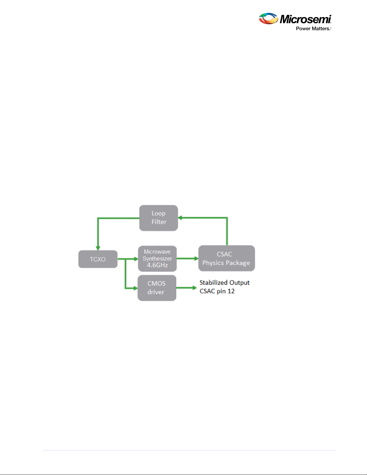
3.3.1 Principle of Operation
The CSAC is a passive atomic clock, incorporating the interrogation technique of coherent population
trapping (CPT) and operating on the D1 optical resonance of atomic cesium. A complete description of
passive atomic clocks, CPT, and the CSAC architecture is beyond the scope of this user guide. The
following illustration shows a simplified block diagram of the CSAC.
Figure 3 • Simplified CSAC Block Diagram
The principal RF output from the CSAC is provided by a temperature-compensated crystal oscillator
(TCXO), which is buffered by a CMOS logic gate and provided on the CSAC output pin 12. In normal
operation, the frequency of the TCXO is continuously compared and corrected to ground state hyperfine
frequency of the cesium atoms, contained in the physics package, which thereby improves the stability
and environmental sensitivity of the TCXO by 4–5 orders of magnitude. In addition to the TCXO and the
physics package , the essential components of the CSAC are the microwave synthesizer and the
1
microprocessor . The microwave synthesizer generates 4596.3x MHz with microprocessor-controlled
2
tuning resolution of approximately 1 × 10 . The microprocessor serves multiple functions, including
–12
implementation of the frequency-lock loop filter for the TCXO, optimization of physics package
operation, state-of-health monitoring, and command and control through RS232.
When the CSAC is initially powered on, it performs an acquisition sequence, which includes stabilizing
the temperature of the physics package, optimizing physics package operating parameters, and
acquiring frequency lock to the atomic resonance. The acquisition process may be monitored through
the field of the telemetry (see ). On power-up, the status status "Telemetry (6 and ^)" (see page 20)
begins at 8 (oven warm-up). The status value decrements numerically through the acquisition until
normal operation (status = 0) is achieved.
SA.45s CSAC User Guide Revision D 6
Page 10
SA.45s Chip-Scale Atomic Clock
1.
2.
R. Lutwak, et. al., The Chip-Scale Atomic Clock - Low-Power Physics Package, Proceedings of the 36th
Annual Precise Time and Time Interval (PTTI) Systems and Applications Meeting, December 7–9,
2004, Washington, DC.
R. Lutwak, et. al., The MAC - A Miniature Atomic Clock, Proceedings of the 2005 Joint IEEE
International Frequency Control Symposium and Precise Time & Time Interval Systems &
Applications Meeting, August 29–31, 2005, Vancouver, BC.
3.3.2 Start-Up Sequence
Caution: To avoid severe damage to the unit, do not apply power to the incorrect terminals. The SA.45s
does not have reverse voltage protection.
When power is connected to pin 7, the SA.45s unit begins its warm-up cycle. A signal appears at the
output once power is applied to the unit. This output signal is not stable until the oscillator is locked
(indicated by the BITE pin at CMOS_low).
After 3 minutes, the CSAC achieves Lock and BITE = 0 ( ). "Built-In Test Equipment (BITE)" (see page 7)
Power consumption during warm-up is greater than during normal operation; it is specified on the CSAC
.datasheet
It is recommended to always allow CSAC to remain powered on for >102 seconds after it acquires LOCK.
102 seconds is the minimum amount of time necessary to save CSAC set points to memory. Otherwise,
upon the next power up, the unit may go in to a mode of operation where it re-acquires all of its set
points; warm-up time will then be out of specification.
3.3.3 Built-In Test Equipment (BITE)
CSAC state-of-health can be monitored electronically on pin 4 (BITE) of the SA.45s CSAC. Frequency lock
is indicated both by status = 0 in the status field of telemetry and by the electrical state of the BITE
output pin, which is high (logic 1) upon initial power-on and whenever status ≠ 0. The BITE pin is a highimpedance CMOS logic output.
Note: When not locked, BITE = 1 and also status ≠ 0 in the status field of the telemetry output string.
At the conclusion of the acquisition sequence (status = 0), BITE remains high for an additional 5 seconds
in order to avoid false indication in the event of acquisition failure. Subsequently, BITE provides an
immediate (within 1 second) indication of lock failure or alarm.
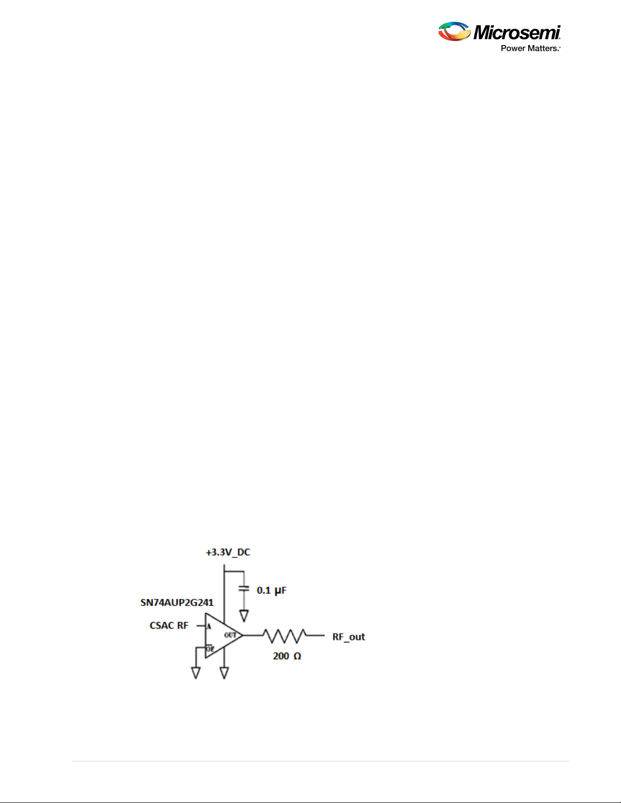
3.3.4 RF Output Characteristics
The buffered CMOS RF output is provided on pin 12 of the SA.45s CSAC. The output series impedance is
200 Ω. For reference, the output driver circuit of the SA.45s is shown in the following illustration.
Figure 4 • CSAC RF Output Driver Circuit
The SA.45s is designed for embedded low-power applications—it is expected to drive a high impedance
input, not a 50 Ω measurement instrument or transmission line.
SA.45s CSAC User Guide Revision D 7
Page 11

SA.45s Chip-Scale Atomic Clock
Note: Driving a 50 Ω line at 13 dBm consumes nearly as much power as the CSAC itself. If a high-level
(high-power) output driver is required, a driver circuit must be implemented external to the CSAC, such
as the one implemented on the Evaluation Board (see )."Notes on the Evaluation Board" (see page 37)
The RF output appears on pin 12 after the CSAC is powered ON and is always present, regardless of the
lock status. When the CSAC is out of lock (BITE = 1, status ≠ 0), the output frequency is provided by the
free-running TCXO, which has frequency accuracy specification of ±20 × 10 and temperature sensitivity
–6
of ≈ ±30 × 10 /°C. Typically, the unlocked frequency accuracy during acquisition is significantly better
–9
than this (<1 × 10 ) as the CSAC memorizes its last-known-good tuning voltage and restores this voltage
–8
upon power-up and/or subsequent recovery from loss-of-lock.
3.3.5 What to Expect During First Power-Up
All CSACs have their output frequency re-centered prior to shipment. However, the shipment conditions
will affect the absolute frequency offset when received by the end-user (temperature excursions,
vibration, duration of transit, and so on). Therefore, some unknown frequency offset should be
expected when the CSAC is first powered on by the user. Offsets may be corrected, as explained in the
following section.
3.3.6 Frequency Steering
Note: CSACdemo is a graphical interface used to communicate and control a CSAC. To display the
functionality of CSAC, screen shots of CSACdemo are included in the sections that follow. For more
information on CSACdemo, see ."CSACdemo Operation" (see page 31)
For external steering and/or calibration, the CSAC internal microwave synthesizer may be adjusted by
the user through the RS232 command (see ). Steering !F "Frequency Adjustment (F)" (see page 23)
values are entered in (integer) units of 1 × 10 , though the resolution realized by the CSAC hardware is
–15
approximately 1 × 10 . Steering commands may be entered as either absolute steers ( ) or as
–12
!FA
relative steers ( ). In the case of an absolute steer, the contents of the steer register are replaced !FD
with the new value. In the case of a relative steer, the new value is summed with the existing value in
the steer register. The maximum steer that can be entered in a single command is ±2 × 10 !FD
–8
(±20000000 × 10 ). The maximum steer that can be entered in a single command is approximately
–15
!FA
±2 × 10 (±2000000000 × 10 ). If a larger value is sent to the CSAC, the maximum allowed steer is
–6 –15
applied.
Caution: It is recommended to limit steering commands to <±2 × 10 increments, to allow the CSAC to
–8
slowly adjust. A larger steer may cause the CSAC to unlock. Do not allow steering to accumulate beyond
the stated datasheet limit.
To overcome the software limit (±2 × 10 ) imposed by the command, the latch command ( )
–8
!FD !FL
will need to be employed (for more information, see ). "Frequency Calibration" (see page 9)
Ultimately, the CSAC steering capability is physically limited by the TCXO tuning voltage. An alarm (see
will trigger when this voltage is breached. Generally, steering the CSAC far from its nominal page 20)
output frequency is undesirable as it will make disciplining difficult, therefore increasing the likelihood
of unlock.
Note: Steering commands may be entered during acquisition (Status ≠ 0) but will not take effect until
lock is achieved.
Frequency steering is volatile. Upon reboot, the CSAC returns to its nominal (calibrated) frequency
setting. To update the non-volatile calibration, use the Frequency Latch command ("Frequency
).Adjustment (F)" (see page 23)
The current steering value appears in the telemetry string as .Steer
Note: Steer reports the actual hardware steering, in units of ×10 , even though the software registers
–12
maintain resolution of ×10 , so that many small relative corrections may be applied. As a result, the
–15
reported value may appear to disagree with the applied correction by one unit or so due to roundoff
error. An example is provided in ."Frequency Adjustment (F)" (see page 23)
SA.45s CSAC User Guide Revision D 8
Page 12
SA.45s Chip-Scale Atomic Clock
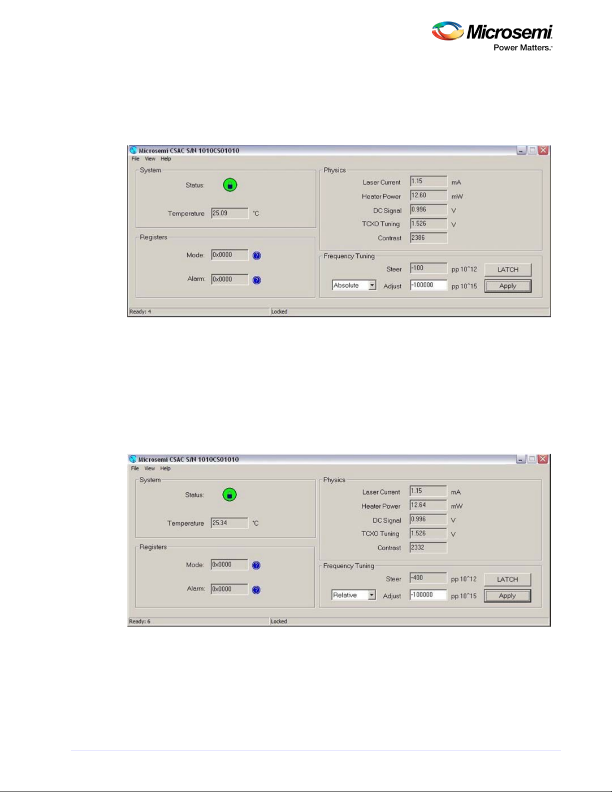
To apply a frequency correction from the main panel of CSACdemo, select relative or absolute from the
pull down menu and enter the desired steering into the Adjust field in ×10 .
–15
The following screen shot shows an example where an absolute correction of –100000 × 10 is
–15
entered. The correction is applied to the CSAC when is selected.Apply
Figure 5 • Absolute Frequency Adjustment
As shown in the previous screen shot, after is clicked, the correction is applied to the CSAC and Apply
the value of Steer changes (on the next polling update) to indicate the internal correction of –100 × 10
–12
.
The following screen shot shows an example of relative frequency tuning after absolute steer is reset to
0. In this example, each time is clicked, an additional correction of –100000 × 10 is applied to Apply
–15
the CSAC. In this screen shot, is clicked a total of four times. The resultant value of Steer is –400 × Apply
10 .
–12
Figure 6 • Relative Frequency Adjustment
3.3.6.1 Frequency Calibration
The internal frequency calibration of the CSAC is set prior to shipment. It is sometimes desirable (and
likely) that the calibration needs to be updated from time to time to remove cumulative frequency aging
offsets.
SA.45s CSAC User Guide Revision D 9
Page 13

SA.45s Chip-Scale Atomic Clock
Calibration of the CSAC is a two-step process. First, the CSAC is steered onto frequency, either through
an external command (see ), through 1PPS disciplining (see !F "Frequency Steering" (see page 8)
), or with analog tuning (see ). Second, "1PPS Disciplining" (see page 12) "Analog Tuning" (see page 14)
the present value of Steer is summed into the non-volatile calibration register through the RS232
Frequency Latch command (see ). Following a Latch "Frequency Adjustment (F)" (see page 23)
command, the value of Steer is reset to zero.
Note: The Latch command is only valid when the CSAC is locked (Status = 0).
To latch the current steer value to non-volatile storage from CSACdemo, click .LATCH
Note: It may be tempting, particularly in disciplining applications, to frequently latch the steering value
into calibration in the event of unforeseen power outage. This is highly discouraged for the following
reason. The lifetime of the CSAC's NV memory is finite; updating it >20,000 times will damage it and
render the CSAC inoperable.
3.3.7 1PPS Output
A CMOS level 1 pulse-per-second (1PPS) output is available on pin 10 upon power-up. The output series
impedance is 200 Ω. The output driver circuit is similar to that of the RF output (see Figure 4 (see page
). Nominal levels are 0 VDC–3.3 VDC. For synchronization purposes, the on-time point is the rising 7)
edge of pin 10.
The 1PPS output is derived by digital division of the RF reference frequency. The frequency stability and
accuracy of the 1PPS output reflects that of the RF output. Consequently, when unlocked (BITE = 1,
status ≠ 0), the 1PPS stability reflects that of the free-running TCXO.
3.3.8 1PPS Synchronization
The 1PPS output is synchronous with one rising edge of the RF output (pin 12). The 1PPS output may be
synchronized with a particular cycle of the RF by applying a synchronization pulse to pin 9. When
synchronized, the counters are reset such that the 1PPS output occurs on the RF rising edge, which is
nearest to the externally-applied rising edge. In this way, the CSAC 1PPS can be synchronized to within
one clock cycle (±100 ns) of the external reference.
The CSAC provides two modes for 1PPS synchronization, Manual and Automatic, which are selected
through a bit in the mode register (see )."Set/Clear Operating Modes (M)" (see page 24)
Note: The configuration of the mode register is non-volatile (preserved across power cycles).
3.3.8.1 Manual Synchronization
In Manual Synchronization mode (default), the CSAC ignores any signal present on the 1PPS input line
(pin 9) until commanded through RS232. When a synchronization command is received (see "1PPS
), the CSAC 1PPS is synchronized to the next rising edge to appear on Synchronization (S)" (see page 25)
pin 9.
This mode is applicable to configurations where the CSAC is embedded in a system where a 1PPS signal
is always present, but not always reliably accurate or stable (such as a GPS receiver). The host
microprocessor may command the CSAC to synchronize after it has verified the state-of-health of the
1PPS reference source (for example, after querying lock state of the GPS receiver).
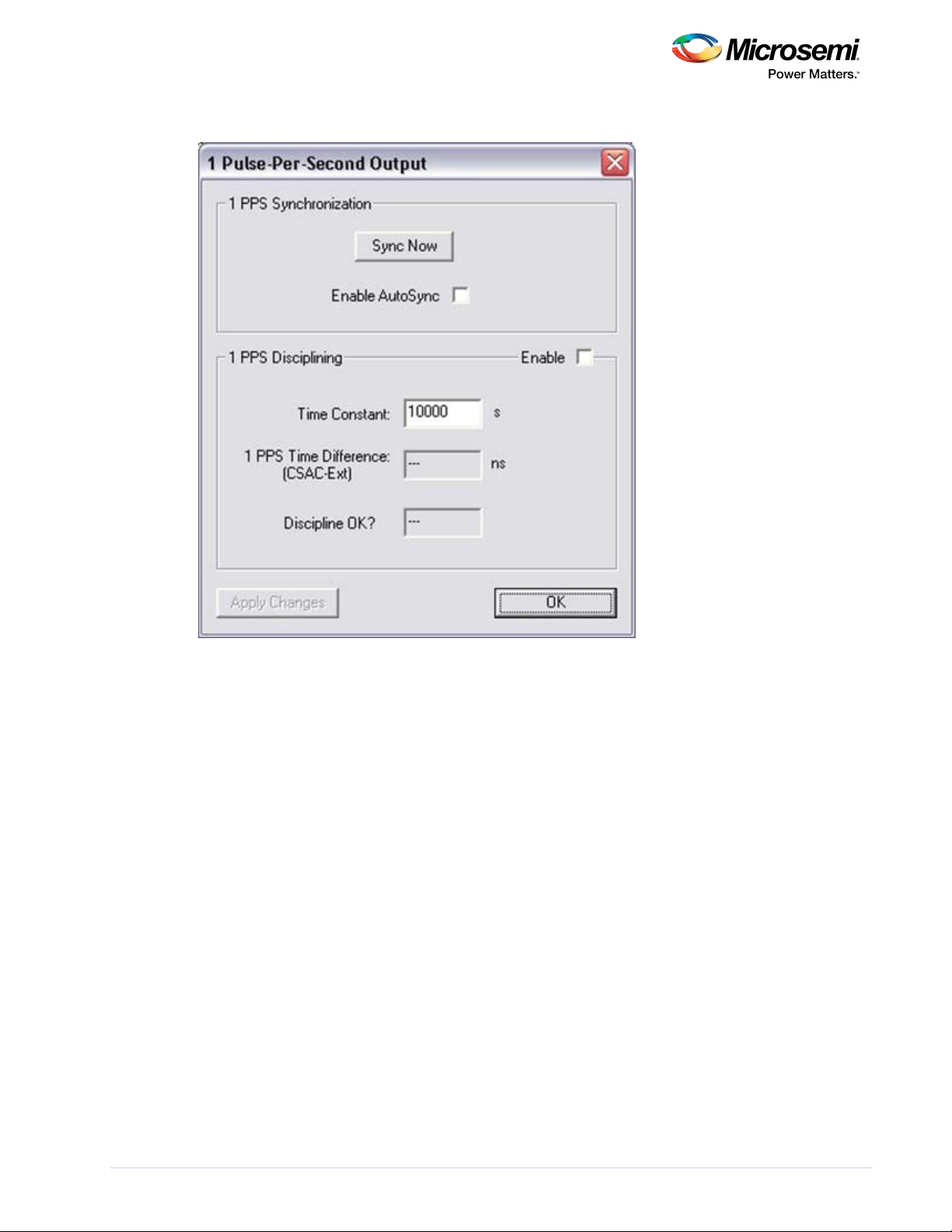
To perform manual synchronization from CSACdemo, open the panel from the menu. The 1PPS… View
1PPS panel is shown in the following screen shot.
SA.45s CSAC User Guide Revision D 10
Page 14
SA.45s Chip-Scale Atomic Clock
Figure 7 • CSACdemo 1 Pulse-Per-Second Output Panel
To manually synchronize the CSAC from CSACdemo, make sure that a valid 1PPS reference is connected
to the 1PPS reference input and click on the 1PPS panel. The CSAC synchronizes to the next Sync Now
rising edge detected on the 1PPS reference input.
3.3.8.2 Automatic Synchronization
In Automatic Synchronization mode, the CSAC synchronizes its 1PPS output to every rising edge that
appears on pin 9. In this mode, synchronization may be performed by connecting a reference 1PPS
signal to pin 9 without needing to issue the RS232 synchronization command. Automatic
synchronization can be enabled/disabled through bit 3 (0x0008) in the mode register (see "Set/Clear
).Operating Modes (M)" (see page 24)
This mode can be useful, for example, in cases where the host system does not communicate with the
CSAC or in which the host system has no method or need to determine the state-of-health of the
reference source.
Note: Automatic Synchronization mode and Disciplining mode (see ) are 1PPS Disciplining (see page 12)
mutually exclusive. Enabling either in the mode register disables the other.
To enable Automatic Synchronization from CSACdemo, select the checkbox on the Enable Autosync
1PPS panel and click (see ).Apply Changes Figure 7 (see page 11)
SA.45s CSAC User Guide Revision D 11
Page 15

SA.45s Chip-Scale Atomic Clock
3.3.9 1PPS Disciplining
A high-resolution phase meter is implemented within the CSAC for improved synchronization (<100 ns)
as well as for frequency calibration of the CSAC. The phase meter measures the time difference between
the internal CSAC 1PPS (pin 10) and the externally applied reference 1PPS (pin 9). The phase meter
measures the relative phase between the CSAC and the reference once per second with a resolution of
450 ps.
Based on the measurements of the phase meter, the disciplining algorithms adjust the CSAC's
microwave synthesizer through the digital tuning value ( , observed from the telemetry string). steer
The algorithm will simultaneously steer both the phase and frequency to that of the external reference,
ultimately achieving accuracies of <5 ns and 5 × 10 , respectively. Note that, unlike the and
–13
!FA !FD
commands, there is no software limitation upon the value of steer.
Disciplining can be enabled/disabled through bit 4 (0x0010) in the mode register (see "Set/Clear
). The time constant of the steering algorithm is user selectable Operating Modes (M)" (see page 24)
through the ID command (see )."Set 1PPS Disciplining Time Constant (D)" (see page 25)
Note: Both mode setting and time constant are non-volatile, that is, preserved across power cycles.
Prior to the onset of steering, the disciplining algorithms first perform an initialization sequence in which
the variables of the steering algorithm are reset to defaults and a 1PPS synchronization operation (see
) is executed to bring the 1PPS output within 100 ns of the "1PPS Synchronization (S)" (see page 25)
reference, thereby avoiding large frequency excursions. Initialization is performed when Disciplining is
first enabled in the mode register and, in the case where Disciplining is already enabled after the CSAC
achieves frequency lock (BITE = 0, status = 0).
In the event that the 1PPS reference is removed from pin 9 while Disciplining, the CSAC remains in
holdover and preserves the most recent steering value. If the 1PPS reference subsequently reappears,
Disciplining continues where it left off, without reinitializing. The notable exception to this is the case in
which the CSAC 1PPS has drifted significantly in phase (>1 μs) from the reference 1PPS during the
outage. In this case a synchronization is performed, though the Disciplining variables are not
reinitialized.
If it is necessary to force re-initialization of the disciplining variables, perhaps because the reference
source is subsequently deemed untrustworthy and subsequently recovers, this can be accomplished by
disabling and re-enabling Disciplining in the mode register (see "Set/Clear Operating Modes (M)" (see
).page 24)
When Disciplining is enabled, the most recent phase meter measurement, rounded to the nearest
nanosecond, is reported in the standard telemetry (see ). The sign "Telemetry (6 and ^)" (see page 20)
of the reported value reflects the measurement of (1PPS_EXT–1PPS_CSAC), that is, if the CSAC 1PPS
rising edge occurs after the external 1PPS rising edge, then the sign is negative.
The status of Disciplining is indicated by the parameter in the telemetry. DiscOK = 0 upon DiscOK
startup. DiscOK = 1 when magnitude of phase measurement is less than phase threshold (see "Set 1PPS
) for two time constants of duration. Phase Threshold for Discipline Status OK Check (m)" (see page 27)
DiscOK = 2 when in holdover (disciplining enabled but no 1PPS present).
Note: Automatic Synchronization mode (see ) and "Automatic Synchronization" (see page 11)
Disciplining mode are mutually exclusive. Enabling either in the mode register disables the other.
In CSACdemo, enabling/disabling Disciplining and setting the discipline time constant are both
accomplished on the 1PPS panel, accessible from the View menu (See ). To Figure 7 (see page 11)
modify the discipline time constant, enter the new value in the field (10–10000) and click
.Apply Changes
SA.45s CSAC User Guide Revision D 12
Page 16

SA.45s Chip-Scale Atomic Clock
3.3.9.1 Cable Length Compensation
The zero point of disciplining can be adjusted to accommodate cable and other instrumentation delays
(or advances) which impact the arrival time of the 1PPS at the CSAC 1PPS input pin. The compensation
value can optionally be stored in the CSAC non-volatile RAM for one-time calibration.
The maximum compensation adjustment is ±100 ns, with resolution of 100 ps. The compensation value
is entered into the CSAC as a signed integer in units of 100 ps, where positive sign indicates phase
advancement of the input 1PPS. For example, if there is 45 ns of delay (approximately 33 feet of RG-58
coaxial cable) between the on-time point and the CSAC 1PPS input then the compensation value would
be +450.
Note: Cable length compensation can also be employed to correct for dynamic known errors in the 1PPS
reference provided, for example, from an external measurement system. For this reason, upon
application the compensation is subsequently applied to the previous 1PPS measurement.
Note: Compensation is implemented in the disciplining algorithm, not in the phase measurement itself.
The phase measurement, as reported through telemetry, reports the actual phase measurement, that is,
if the CSAC is disciplined with +50 ns of compensation, the phase meter reports –50 ns of phase error.
Compensation is set with the command (see !DC "Set 1PPS Disciplining Cable Length Compensation
).(DC)" (see page 27)
3.3.10 Time-of-Day
The CSAC maintains time-of-day (TOD) as a 32-bit unsigned integer, which is incremented synchronously
with the rising edge of the 1PPS output. Until set otherwise, TOD begins counting from zero when the
CSAC is powered on.
TOD is retrieved from the CSAC over RS232 with the command (see !T? Time-of-Day (TOD) (see page
). When the command is received, the CSAC waits for the next rising edge of 1PPS before 26) !T?
replying with the TOD of the current epoch, that is, if the command is received during epoch N, then the
reply N+1 appears immediately following the next 1PPS. This strategy provides the host system with
minimum ambiguity in interpreting the response.
TOD can be set with the command through the RS232 interface. The command includes provision !T !T
both for setting an absolute number or for a differential (±) adjustment of the present TOD. An example
is provided in the . To avoid ambiguity in setting the TOD, it is Time-of-Day section (see page 26)
recommended that the host system wait for 1PPS and transmit the setting/adjustment immediately
thereafter.
The CSACdemo program shows TOD on the Time Of Day panel, accessed from the View menu, as shown
in the following screen shot.
SA.45s CSAC User Guide Revision D 13
Page 17

SA.45s Chip-Scale Atomic Clock
Figure 8 • CSACdemo Time-of-Day Panel
The raw CSAC TOD value is shown in the lower field of the panel (here 1260881710). The upper display
of the TOD panel realizes the timekeeping convention of the C programming language (in UNIX and
Microsoft Windows), which counts time in seconds from midnight on January 1, 1970. Upon clicking
, it sets the CSAC time according to the host PC's TOD counter (either local time or UTC depending Send
on the setting of the pull-down menu to the left of the ). The and buttons for hours and seconds Send + adjustment will increment or decrement the CSAC TOD by ±3600 or ±1 second respectively.
3.3.11 Analog Tuning
To enable analog frequency tuning for implementation in legacy (quartz crystal) applications, the
frequency of the CSAC can be tuned with an external voltage applied to pin 1. This functionality can be
enabled/disabled through a bit in the mode register (see "Set/Clear Operating Modes (M)" (see page 24
). The applied voltage is digitized by an internal analog-to-digital converter and the correction is applied )
to the microwave synthesizer at a rate of once per second, that is, the maximum tuning rate is 1 Hz.
When analog tuning is enabled, the voltage applied at pin 1 and the resultant steering are reported in
the standard telemetry stream (see ). The tuning voltage input "Telemetry (6 and ^)" (see page 20)
range is 0 VDC–2.5 VDC, which corresponds to a full scale tuning range of 4.4 ×10 . Nominal zero-
–8
correction tuning occurs at a tuning input voltage of 1250 mV. The fractional frequency correction, for a
given applied voltage, is given by the following equation.
Δf/f = (V – 1250 mV) × 1.77× 10 /mVtune
–11
Note: This formula is accurate for the standard SA.45s CSAC, operating at 10.0 MHz output frequency.
Consult the datasheet for tuning curves of CSACs at alternate frequencies. The tuning input pin is
nominally biased at ≈1250 mV, that is, approximately zero correction.
Note: Bias voltage may vary due to component variations and/or exhibit temperature sensitivity.
Therefore, analog tuning should not be enabled unless the functionality is necessary and the analog
tuning input pin is connected to a low noise, low impedance voltage source. For non-legacy applications,
it is recommended that this feature remain disabled, and that corrections be applied through the digital
communications interface (see ) to avoid degradation of the CSAC "Frequency Steering" (see page 8)
short-term stability due to voltage noise applied to the tuning pin.
Analog tuning can be enabled/disabled and monitored from the CSACdemo application from the Analog
Tuning… panel (accessible from the View menu), as shown in the following screen shot.
SA.45s CSAC User Guide Revision D 14
Page 18

SA.45s Chip-Scale Atomic Clock
Figure 9 • CSACdemo Analog Tuning Panel
When analog tuning is enabled, the voltage present on pin 1 is displayed in the Analog Tuning field and
also reflected in the current reported value of steer on the main panel. To enable or disable analog
tuning, select checkbox and click .Enable Analog Tuning Apply Changes
3.3.12 Ultra-Low Power Operating Mode
The majority of the power in the CSAC is consumed by the physics package and microwave synthesizer.
In ultra-low power (ULP) mode, the physics package and synthesizer can be disabled for a user-specified
length of time, during which the CSAC operates as a free-running TCXO. Periodically, the atomic clock
portion of the CSAC is powered on (again for a user-specified amount of time) and the TCXO is recalibrated to the atomic frequency. Operating in this mode, the CSAC exhibits the short-term
performance of a TCXO with good long-term stability at significantly lower power compared to standard
mode. For example, if the atomic clock portion is only powered on for 5 minutes out of every hour (2
minutes for lock acquisition + 3 minutes of run time), then the time-averaged power of the CSAC may be
<30 mW.
Between calibration cycles, the CSAC in ULP mode exhibits the performance characteristics of a freerunning TCXO and therefore exhibits significantly higher short-term frequency drift and environmental
(temperature and vibration) sensitivity than a normally-operating CSAC. For this reason, ULP mode is
principally recommended only for applications that:
Require long-term timing performance, rather than short-term frequency or time stability.
Have a very stable environment (temperature and vibration).
Note: Due to the unique behavior and configurability of ULP, the datasheet performance specifications
for the SA.45s CSAC cannot be guaranteed while in ULP mode. The CSAC has short-term drift
performance of a low cost low performance TCXO. Contact Microsemi for additional assistance in
evaluating and optimizing ULP for your specific application.
The following illustration shows an example of a CSAC operating in ULP mode, with wake-time = 300 s (5
min) and sleep-time = 3300 s (55 min).
SA.45s CSAC User Guide Revision D 15
Page 19

SA.45s Chip-Scale Atomic Clock
Figure 10 • Frequency Record of CSAC in ULP Mode
The green arrows indicate the on time calibrations. Note the relatively poor TCXO drift and temperature
behavior between calibrations.
ULP is an unusual operating mode for an atomic clock and it is important for the user to understand
exactly how the clock is behaving to effectively implement this feature in a system. In particular, note
the following:
When operating in ULP mode, the Status register indicates Status = 9 (asleep) when the atomic clock
portion of the CSAC is asleep. Each wake cycle is indicated by the usual lock process (Status = 8, 7, 6,
…) followed by wake-time seconds of operation at Status = 0 before the cycle repeats. This cycle is
also reflected on the BITE pin, which is 1 (high) whenever the CSAC is unlocked (or asleep) and only
0 (low) during the locked periods.
When using Disciplining (see ) in conjunction with ULP, disciplining "1PPS Disciplining" (see page 12)
functionality is disabled during sleep and unlocked cycles, though steering information is preserved
and updated across wake cycles.
Frequency Steering commands may be entered when the CSAC is asleep or unlocked but do not
affect the output frequency until lock is achieved, typically on the next wake cycle (see "Frequency
). Also, the Latch command is only valid when the CSAC is lockedSteering" (see page 8)
(Status = 0).
If enabled, Analog Tuning (see ) is only active during wake cycles."Analog Tuning" (see page 14)
ULP is enabled through bit 5 (0x0020) in the mode register (see "Set/Clear Operating Modes (M)" (see
) and the sleep-time and wake-time are set by the command (see page 24) !U "Set Ultra-Low Power
). These values are non-volatile; they persist across power cycles. Mode Parameters (U)" (see page 26)
Note that the wake-time begins counting after the CSAC achieves lock, so the actual time that the
atomic clock portion of the CSAC is powered on is the sum of the time to lock and the user-configured
wake-time. The minimum allowed values of wake-time and sleep-time are 10 seconds and 1800
seconds, respectively.
To configure ULP parameters using CSACdemo, select from the View menu to Ultra-Low Power Mode
access the panel shown in the following screen shot.
SA.45s CSAC User Guide Revision D 16
Page 20

SA.45s Chip-Scale Atomic Clock
Figure 11 • CSACdemo Ultra-Low Power Mode Configuration Panel
Enter the desired settings and click to upload new settings to the CSAC.Apply Changes
3.3.13 1PPS Phase Measurement Mode
For firmware versions 1.08 and later, an additional phase meter is implemented with extended range
(±500 ms) to measure the time difference between the internal CSAC 1PPS (pin 10) and the externally
applied reference 1PPS (pin 9). Measurement resolution is approximately 100 ns.
Note: 1PPS phase measurement mode utilizes both the extended-range phase meter and the highresolution phase meter (450 ps resolution) used in 1PPS Disciplining (see "1PPS Disciplining" (see page
). In this mode, the phase measured by the high-resolution meter is reported if phase is in the range 12)
±1 µs (approximate), otherwise the extended-range meter is reported.
Phase measurement mode may be enabled/disabled through bit 2 (0x0004) in the mode register (see
). Phase Measurement mode, Automatic "Set/Clear Operating Modes (M)" (see page 24)
Synchronization, and Disciplining are all mutually exclusive, so enabling a 1PPS-related option in the
mode register disables the other 1PPS-related options.
3.4 Programmers Reference
Pins 5 and 6 provide a serial interface for communication with the CSAC. The protocol is fundamentally
similar to RS232, with the exception that the voltage levels are CMOS (0–VCC), rather than ±12 V.
The data rate and word structures are as follows:
57,600 Baud
8 data bits
No parity
1 stop bit (8-N-1)
No flow control
For interfacing with a standard RS232 controller interface, which requires ±12 V logic levels, an external
level shifter must be employed, such as the Maxim MAX202 employed on the evaluation board (see
)."Notes on the Evaluation Board" (see page 37)
3.4.1 Overview of Telemetry Interface
The CSAC communicates exclusively with printable (non-binary) ASCII characters.
SA.45s CSAC User Guide Revision D 17
Page 21

SA.45s Chip-Scale Atomic Clock
In general, commands are to be preceded by an exclamation point ( ) and followed by a carriage-return!
/linefeed pair (ASCII 0x0D 0x0A). For convenience and efficiency, most commands also provide [CRLF]
a single-character shortcut, which is executed immediately, that is without bracketing by and . ! [CRLF]
For example, the single character shortcut is functionally identical to .^ !^[CRLF]
After transmitting but prior to sending , a command may be aborted by sending the escape ! [CRLF]
character (ASCII 0x1B).
All commands produce a response from the CSAC, which are human readable, with individual lines
ending in . If an unsupported or improperly formatted command is received, the CSAC responds [CRLF]
with .?[CRLF]
3.4.1.1 Checksum (Error-Checking Option for Telemetry Interface Communications)
For improved communications reliability, an NMEA-style checksum may be enabled through bit 6
(0x0040) of the mode register (see ). When enabled, "Set/Clear Operating Modes (M)" (see page 24)
the checksum is required for all input commands and is present on all replies from the CSAC.
The checksum is a two-byte ASCII representation (in hexadecimal) of the XOR of all characters in the
command between—but not including—the and the characters. The checksum is preceded ! [CRLF]
by a * character and appended to the command immediately prior to the . Because commands [CRLF]
including checksum are inherently multi-character, single-character shortcuts are not available when
checksum is enabled.
Example (enable analog tuning through mode register):
Command: !MA*0C[CRLF]
Unit response: 0x0041*4D[CRLF]
Example (disable checksum through mode register)
Command: !Mc*2E[CRLF]
Unit response: 0x0000[CRLF]
If the checksum is not present or if the checksum value is invalid, then the command is not executed and
the CSAC responds with .*[CRLF]
Example (malformed checksum):
Command: !Mc*2D[CRLF]
Unit response: *[CRLF]
To experiment with checksum in CSACdemo and observe the calculated checksums in the Trace window,
select checkbox on the Options… panel, as shown in the following screen shot.Require Cksum
SA.45s CSAC User Guide Revision D 18
Page 22

SA.45s Chip-Scale Atomic Clock
Figure 12 • CSACdemo Options… Panel
3.4.1.2 How to Calculate the Checksum
Checksum value is a two digit hexadecimal representation of the logical XOR of each character in the
command (excluding “ ” and “ ”). For example, if one desires to implement analog tuning by ! [CRLF]
sending the command, then they should send in Checksum mode. In !MA[CRLF] !MA*0C [CRLF]
the following table, we convert and to their binary equivalents and calculate the XOR in the bottom M A
row. The corresponding hexadecimal value of that XOR is “C”. Therefore the two-digit Checksum is
“ ”.0C
Table 4 • Checksum Calculation Example
Checksum Components ASCII Character Binary Value Hex Value
Input command characters M 1001101
A 1000001
Logical XOR 0001100 C
3.4.2 Command Summary
The following table summarizes the CSAC commands.
Note: The and commands are only available for firmware versions 1.08 and later.m >
SA.45s CSAC User Guide Revision D 19
Page 23

SA.45s Chip-Scale Atomic Clock
Table 5 • Command Summary
Shortcut Description Command Reference Section
6 Return telemetry headers
as comma-delimited string
!6[CRLF] "Telemetry (6 and ^)" section
(see page 20)
^ Return telemetry as
comma-delimited string
!^[CRLF] "Telemetry (6 and ^)" section
(see page 20)
F Set/report frequency
adjustment
!F?[CRLF] "Frequency Adjustment (F)"
section (see page 23)
M Set/report operating mode
register bits
!M?[CRLF] "Set/Clear Operating Modes
(M)" section (see page 24)
S Sync CSAC 1PPS to external
1PPS
!S[CRLF] "1PPS Synchronization (S)"
section (see page 25)
D Set/report 1PPS
disciplining time constant
!D?[CRLF] "Set 1PPS Disciplining Time
Constant (D)" section (see page
25)
U Set/report ultra-low power
mode parameters
!U?[CRLF] "Set Ultra-low Power Mode
Parameters (U)" section (see
page 26)
T Set/report time-of-day !T?[CRLF] "Time-of-Day (TOD)" section
(see page 26)
m Set/report 1PPS phase
threshold for discipline
status OK check
!m?[CRLF] "Set 1PPS Phase Threshold for
Discipline Status OK Check (m)"
section (see page 27)
> Set/report 1PPS Out Pulse
width as multiple of
default width
!>?[CRLF] "Set 1PPS Out Pulse Width as an
Integer Multiple of Default
Width (>)" section (see page 28)
@ Set/report deferred
command
!@?[CRLF] "Deferred Command (@)"
section (see page 28)
? Help !?[CRLF] "Help (?)" section (see page 28)
3.4.3 Detailed Command Descriptions
The following are descriptions of the CSAC's commands.
3.4.3.1 Telemetry (6 and ^)
CSAC supports two commands, and , to retrieve the telemetry headers and values, respectively. !6 !^
Both responses are comma-delimited strings, suitable for importing into spreadsheet programs.
Example:
Telemetry headers command: !6[CRLF]
Unit response: Status,Alarm,SN,Mode,Contrast,LaserI,TCXO,HeatP,Sig,Temp,
Steer,ATune,Phase,DiscOK,TOD,LTime,Ver[CRLF]
Example:
Telemetry data command: !^[CRLF]
Unit response: 0,0x0000,1209CS00909,0x0010,
4381,0.86,1.573,17.62,0.996,28.26,- 24,---,-1,1,1268126502,586969,1.0
[CRLF]
The maximum length of a telemetry string is 135 characters.
SA.45s CSAC User Guide Revision D 20
Page 24

SA.45s Chip-Scale Atomic Clock
1.
2.
The maximum length of a telemetry string is 135 characters.
Note: The single-characters and are shortcuts for and , respectively.6 ^ !6[CRLF] !^[CRLF]
The following table lists the telemetry parameters and their associated header identifiers.
Table 6 • Telemetry Parameters (Firmware Version 1.09)
Identifier Description Notes String Length
Status Unit status See Note 1 and Table 7 (see
page 22)
Up to 2 decimal digits (2 characters)
Alarm Pending unit
alarms
See Note 2 and Table 8 (see
page 22)
“0x” + 4 hexadecimal digits (6
characters max)
SN Unit serial number See Note 3 11 characters
Mode Mode of
operation
See Table 9 (see page 24) “0x” + 4 hexadecimal digits (6
characters max)
Contrast Indication of
signal level
Typically >2000 when locked,
and ≈ 0 when unlocked
32 bits unsigned (10 characters max)
LaserI Laser current (mA) Typically 0.6 mA–1.3 mA 16 bits unsigned + “.” + 2 digits
precision (8 characters max)
TCXO Tuning voltage (V) 0 VDC–2.5 VDC tuning range
≈ ±10 × 10
6
16 bits unsigned + “.” + 3 digits
precision (9 characters max)
HeatP Physics package
heater power
(mW)
Typical 6 mW–20 mW under
normal operating conditions
and 25 °C ambient
16 bits unsigned + “.” + 2 digits
precision (8 characters max)
Sig DC signal level (V) Typical 0.8 V–1.7 V under
normal operating conditions
16 bits unsigned + “.” + 3 digits
precision (9 characters max)
Temp Unit temperature
(°C)
Absolute accuracy is ±2 °C 16 bits unsigned + “.” + 2 digits
precision (8 characters max)
Steer Frequency adjust In ×10 resolution
–12
32 bits signed (11 characters max)
ATune Analog tuning
voltage input
--- when analog tuning is
disabled, 0 V–2.5 V when
enabled
16 bits unsigned + “.” + 3 digits
precision (9 characters max)
Phase Difference
between CSAC
and external 1PPS
(ns)
Only present if discipline or
phase-measure mode
enabled, otherwise or --NEEDREFPPS
16 bits signed (6 characters max)
DiscOK Discipline status
(0-2)
0 = acquiring, 1 = locked, 2 =
holdover when disciplining
enabled, otherwise ---
“0", “1", “2" or “---“ (3 characters
max)
TOD Time (seconds) Starts at 0 upon power-up
unless set by command
32 bits unsigned (10 characters max)
LTime Time since lock
(seconds)
Starts at 0 upon lock 31 bits unsigned (10 characters max)
FWver Firmware version Two digit number M.m
where M is major revision
and m is minor revision
“1.09” (4 characters, may be longer
in future firmware)
Notes:
Status reflects the steps of the clock initialization process. It starts at 8 on boot and decreases to 0 as
acquisition proceeds. When Status ≠ 0, BITE = 1. When Status = 0, BITE = 0.
Alarms indicate detection of anomalous operating conditions while locked. Alarm is the logical OR of
all pending alarms, as shown in the following table. An alarm will not persist if the condition is fixed
or if the unit is reset.
SA.45s CSAC User Guide Revision D 21
Page 25

SA.45s Chip-Scale Atomic Clock
3. CSAC serial numbers are of the form YYMMCSXXXXX where YYMM is the year and month of
production and XXXXX is the serialized production unit number.
Table 7 • Status Codes of CSAC
Status Acquisition Stage
9 Asleep (ULP mode only)
8 Initial warm-up
7 Heater equilibration
6 Microwave power acquisition
5 Laser current acquisition
4 Laser power acquisition
3 Microwave frequency acquisition
2 Microwave frequency stabilization
1 Microwave frequency steering
0 Locked
Note: If CSAC returns a status code other than shown in , then it is re-acquiring its Table 6 (see page 21)
set points. In this case, warm-up time takes longer than stated on the SA.45s datasheet. To avoid this, it
is recommended to always allow CSAC to remain powered on for >102 seconds after it acquires LOCK.
102 seconds is the minimum amount of time necessary to save CSAC set points to memory, thus
avoiding set-point re-acquisition upon its next power up.
Table 8 • Alarm Codes of CSAC
Alarm Definition Alarm Limit
0x0001 Signal contrast low Contrast <1000
0x0002 Synthesizer tuning at limit Synthesizer detuned from calibration by
>30 kHz or <–15 kHz
0x0004 Temperature bridge unbalanced Bridge—set-point >±20 mV
0x0010 DC light level low Set-point—DCL > 1.5 V
0x0020 DC light level high DCL—set-point > 1.5 V
0x0040 Heater voltage low <30 mV
0x0080 Heater voltage high >2.48 V
0x0100 µW power control low <20 mV
0x0200 µW power control high >2.48 V
0x0400 TCXO control voltage low <0.1 V
0x0800 TCXO control voltage high >2.4 V
0x1000 Laser current low <0.5 mA
0x2000 Laser current high >2.3 mA
0x4000 Stack overflow (firmware error)
SA.45s CSAC User Guide Revision D 22
Page 26

SA.45s Chip-Scale Atomic Clock
3.4.3.2 Frequency Adjustment (F)
The output frequency of the CSAC may be adjusted (steered) through RS232. The internal resolution of
the fractional frequency correction is approximately 1 × 10 . The correction is entered in integer units
–12
of ×10 . The maximum allowed correction in a single command is ±20000000 (2 × 10 ). The
–15
!FD
–8
maximum allowed correction in a single command is approximately ±2000000000 (2 × 10 ). !FA
–6
Corrections may be applied as either Absolute or Relative, depending on the first character following the
, that is or for absolute or relative (delta) respectively. In the case of absolute steering, the !F !FA !FD
value of the Steer register is replaced with the new value. In the case of relative (delta) steering, the
new value is summed with the existing value in the Steer register, that is, two relative corrections of
–10000 result in a total offset of –2 × 10 . The current steering value is reported in the field of
–11
steer
the telemetry in units of ×10 .
–12
The format for the Adjust frequency command is !FYXXXXX[CRLF]
where Y is either A or D and XXXXX is the new correction in ×10 .
–15
Example (apply absolute tuning correction of –1.23 × 10 ):
–10
Command: !FA-123000[CRLF]
Unit response: Steer = -123[CRLF]
Example (apply delta tuning correction of –1.23 × 10 ):
–10
Command: !FD-123000[CRLF]
Unit response: Steer = –246[CRLF]
Example (report current value of ):steer
Command: !F?[CRLF]
Unit response: Steer = –246[CRLF]
Note: That the single-character is a shortcut for .F !F?[CRLF]
The contents of the Steer register are volatile, that is, the Steer is reset to 0 when power is cycled to the
CSAC. In many cases, it is desirable to preserve the steer upon power-down (for example, calibration of
the CSAC). This is accomplished by sending a Frequency Latch command to the CSAC, which updates the
internal calibration (stored in non-volatile memory) according to the current value of the Steer register
and resets Steer to zero. Note that the Latch command is only valid when the CSAC is locked (Status = 0).
Example:
Command: !FL[CRLF]
Unit response: Steer Latched [CRLF] Steer = 0[CRLF]
Once a Latch command is issued, the previously latched value cannot be recovered. There is no
command to restore “factory defaults”.
Note: The frequency steering command ( ) is recommended for real-time disciplining of CSACs, but !F
the value should not be latched ( ) on every steer due to the physical limit on the number of times !FL
the non-volatile memory may be written before damage (20,000). For example, if an command was !FL
applied to the CSAC, accompanying a steer ( ), at a rate of 1/sec, the CSAC may experience !F
operational failure within 8 hours.
SA.45s CSAC User Guide Revision D 23
Page 27

SA.45s Chip-Scale Atomic Clock
3.4.3.3 Set/Clear Operating Modes (M)
Operating modes of the CSAC are enabled/disabled by individual bits in the mode register. The !M
command provides access to set/clear each of the bits independently. The mode register is non-volatile;
settings persist across power cycles.
The unit responds by reporting the current value of the mode register in hexadecimal. Each bit in the
mode register is associated with enabling/disabling a particular operating mode. The bit assignments are
shown in the following table.
Table 9 • Operating Modes of CSAC
Enable Bit Assignment Enable Argument to !M_ Definition Disable Argument to !M_
0x0001 A Analog tuning a
0x0002 Reserved
0x0004 M 1PPS phase
measurement (only
available on firmware
versions 1.08 and later)
m
0x0008 S 1PPS auto-sync s
0x0010 D Discipline d
0x0020 U Ultra-Low Power mode u
0x0040 C Require checksum on !
command
c
0x0080 Reserved
? Report current settings
Example (Enable and then Disable analog tuning):
Command: !MA[CRLF]
Unit response: 0x0001[CRLF]
Command: !Ma[CRLF]
Unit response: 0x0000[CRLF]
The current value of the mode register is returned in the standard telemetry query (see "Telemetry (6
) or may be queried independently with the command.and ^)" (see page 20) !M?
Example (query mode register):
Command: !M?[CRLF]
Response: 0x0001[CRLF]
Note: That the single-character is a shortcut for .M !M?[CRLF]
Autosync mode, Discipline mode, and Phase Measurement mode (if mode available in the firmware
version) are mutually exclusive. Setting a 1PPS-related option automatically disables the other 1PPSrelated options.
SA.45s CSAC User Guide Revision D 24
Page 28

SA.45s Chip-Scale Atomic Clock
3.4.3.4 1PPS Synchronization (S)
To synchronize the 1PPS output (pin 10) to an externally applied 1PPS synchronization input (pin 9),
connect the external 1PPS signal to pin 9 and send the command. The rising edge of the 1PPS output !S
will synchronize to within ±100 ns (approximately) of the next rising edge of the 1PPS input. If a valid
1PPS input does not appear at the 1PPS input within 3 seconds, the operation is aborted and an error is
returned.
Example (synchronize 1PPS):
Command: !S[CRLF]
Unit response: S[CRLF]
or: E[CRLF]
The unit response (S or E) occurs after either successful synchronization or 3-second timeout. This
permits the host system to verify successful synchronization.
Note: The single-character is a shortcut for .S !S[CRLF]
3.4.3.5 Set 1PPS Disciplining Time Constant (D)
The time constant for disciplining to an externally-supplied 1PPS reference source may be selected to
provide optimal performance in a given application (see )."The Art of Disciplining" (see page 35)
The time constant can range between 10 to 10000 seconds. The 1PPS disciplining time constant is set
with the command. The format for setting the time constant is !D !DX[CRLF]
where X is the new time constant in seconds.
Example (set disciplining time constant to 80 seconds):
Command: !D80[CRLF]
Response: 80[CRLF]
To query the current time constant setting, without modifying the value, use the command !D?
Example (query current disciplining time constant):
Command: !D?[CRLF]
Response: 80[CRLF]
Note: The single-character is a shortcut for .D !D?[CRLF]
3.4.3.6 Set 1PPS Disciplining Cable Length Compensation (DC)
Cable length compensation can be applied to allow for known delay (or advance) in the arrival time of
the reference 1PPS at the CSAC (see ). Cable length "Cable Length Compensation" (see page 13)
compensation is represented as a signed integer in units of 100 ps, with a maximum value of ±1000
(100 ns).
The sign of the compensation is such that a positive value reflects known DELAY in the arrival time of
the 1PPS. For instance, 33 feet of RG-58 cable requires compensation of +45 ns.
The format for setting the cable length compensation value is !DCX[CRLF]
where X is the new compensation value.
Example (set cable length compensation to +15 nanoseconds):
SA.45s CSAC User Guide Revision D 25
Page 29

SA.45s Chip-Scale Atomic Clock
Command: !DC150[CRLF]
Response: 150[CRLF]
To query the current compensation setting, without modifying the value, use the command !DC?
Example (query current compensation setting):
Command: !DC?[CRLF]
Response: 150[CRLF]
To store the current compensation setting in non-volatile RAM, use the command !DCL
Example (Latch current value of compensation to power-up default):
Command: !DCL[CRLF]
Response: Phase comp latched[CRLF]
3.4.3.7 Set Ultra-Low Power Mode Parameters (U)
Note: Placing the CSAC in ULP mode results in short-term drift performance of its internal TCXO.
The ultra-low power operating mode is defined by two parameters, Sleep-Time and Wake-Time, which
may be set with the command in this format: !U !USSS, WWW[CRLF]
where SSS is the sleep time in seconds and WWW is the wake time in seconds.
Example (set sleep time = 55 minutes, wake time = 5 minutes):
Command: !U3300,300[CRLF]
Response: 3300,300[CRLF]
The allowed ranges of Sleep-Time and Wake-Time are 1800 seconds to 65535 seconds and 10 seconds
to –65535 seconds, respectively.
To query the ULP settings without modifying their values, use the command .!U?
Example (query current ULP settings):
Command: !U?[CRLF]
Response: 3300,300[CRLF]
Note: The single-character is a shortcut for .U !U?[CRLF]
3.4.3.8 Time-of-Day (TOD)
TOD is maintained internally within the CSAC, represented by a single unsigned long integer value,
which begins counting up from 0 when the CSAC is powered on. The TOD is synchronized with the 1PPS
output. TOD is routinely transmitted in the telemetry string (see )."Telemetry (6 and ^)" (see page 20)
TOD may be set externally with the command in this format: !T !TYXXXX[CRLF]
where Y is either A for absolute setting or D for a delta adjustment of TOD and XXXX is either the
unsigned integer TOD (typically either UNIX/Windows time or GPS time) or a signed integer adjustment
to the TOD.
Example (absolute setting TOD to 1221578499):
SA.45s CSAC User Guide Revision D 26
Page 30

SA.45s Chip-Scale Atomic Clock
Command: !TA1221578499[CRLF]
Unit response: TimeOfDay = 1221578499[CRLF]
Example (retard TOD by 3600 seconds = 1 hour):
Command: !TD-3600[CRLF]
Unit response: TimeOfDay = 1221574902[CRLF]
The TOD may be reported synchronous with the 1PPS output:
Example (retrieve TOD command):
Command: !T?[CRLF]
Unit Response: XXXX[CRLF]
where XXXX is the current TOD.
Note: This response does not occur until the next 1PPS output pulse.
When queried with the command, the first character of TOD appears on RS232 within 20 ms of the !T?
rising edge of the next 1PPS output pulse. Because this necessarily creates a delay of up to a second
between sending the command and receiving a response from the CSAC, the host system must !T?
allow for an RS232 receive timeout of at least 1000 ms when anticipating a response to the !T?
command. For less critical timing applications, the TOD can be somewhat ambiguously parsed from the
standard telemetry string (see )."Telemetry (6 and ^)" (see page 20)
Note: The single-character is a shortcut for .T !T?[CRLF]
3.4.3.9 Set 1PPS Phase Threshold for Discipline Status OK Check (m)
The 1PPS phase threshold (for discipline status OK check) when disciplining to an externally-supplied
1PPS reference source may be configured to provide optimal performance in a given application.
For applications with a long disciplining time constant and a noisier 1PPS reference (such as GPS), there
could be large variations in the reported 1PPS phase of a CSAC disciplined ok (checked through ADEV
measurement) but the phase threshold being set to a larger value ensures the DiscOK = 1 indication is
set correctly (see )."1PPS Disciplining" (see page 12)
For applications with a short disciplining time constant, the phase threshold can be set to a smaller
value. The range of 1PPS Phase Threshold for Discipline Status OK Check is 1 nanosecond to 10
9
nanoseconds (absolute values), with a default of 20 nanoseconds.
To set the phase threshold (for Discipline Status OK Check), the command has this format: !mX[CRLF]
where X is the new phase threshold's magnitude/absolute value in nanoseconds.
Example (set 1PPS phase threshold for discipline status OK Check to ±20 nanoseconds):
Command: !m20[CRLF]
Response: 20[CRLF]
To query the 1PPS phase threshold setting, without modifying the values, use the command .!m?
Example (query current 1PPS Phase Threshold setting):
Command: !m?[CRLF]
Response: 20[CRLF]
SA.45s CSAC User Guide Revision D 27
Page 31

SA.45s Chip-Scale Atomic Clock
Note: The single-character is a shortcut for .m !m?[CRLF]
3.4.3.10 Set 1PPS Out Pulse Width as an Integer Multiple of Default Width (>)
CSAC's 1PPS output (pin 10) has a default pulse width that may not be sufficiently long for certain
applications. In such cases, the pulse width can be set to an integer times the default pulse width by
using the command with this format: !> !>X[CRLF]
where X is the unsigned integer used as a multiple of the default 1PPS Out Pulse Width to set the
desired 1PPS Out's Pulse Width.
The allowed range of 1PPS Out Pulse Width integer multiple of default Pulse Width is from 1 to 4.
Example (set 1PPS Out Pulse Width as a 2x multiple of default Pulse Width):
Command: !>2[CRLF]
Response: PPS Pulse Width = 2 times ~100 usec [CRLF]
Note: The default pulse width is dependent on the selected frequency option for RF output (pin 12).
When RF output frequency of 10 MHz (option 001) is selected, then the 1PPS out pulse width default is
~100 microseconds, while for other RF output frequency option's the 1PPS out pulse width is as
specified on the datasheet.
To query the 1PPS Out Pulse Width setting, without modifying the values, use the command .!>?
Example (query current 1PPS Out Pulse Width setting):
Command: !>?[CRLF]
Response: PPS Pulse Width = 4 times ~100 usec[CRLF]
Note: The single-character is a shortcut for .> !>?[CRLF]
3.4.3.11 Deferred Command (@)
Any command can be sent at a deferred time by using the command with this format:!@
!T@XXXX,YYYY[CRLF]
where XXXX is the deferred time in seconds and YYYY is the command that is sent after the deferred
time.
Example (defer sending the command by 10 seconds):6
Command: !@10,6[CRLF]
Unit response: Deferred = 10,6
Unit response (after 10 seconds): Status,Alarm,SN,Mode,Contrast,LaserI,TCXO,HeatP,
Sig,Temp,Steer,ATune,Phase,DiscOK,TOD,LTime,Ver
3.4.3.12 Help (?)
The following table lists all available commands in response to the command.?
SA.45s CSAC User Guide Revision D 28
Page 32

SA.45s Chip-Scale Atomic Clock
Table 10 • Unit Response to Help Command (?)
Command Description
F- Adjust frequency
^- Telemetry
6- Telemetry headers
D- Set 1PPS discipline tau
m- Set 1PPS discipline threshold for phase in ns
>- Set 1PPS out pulse width as 1–4 times default
S- Sync 1PPS
U- Set parameters for ultra-low power mode
M- Change mode register
T- Change/report time of day
?- Show this list
@- Delayed command execution
For firmware versions 1.08 and later, the response also contains the above lines on and commands.m >
Note: The single-character is a shortcut for .? !?[CRLF]
3.5 Developer's Kit
The CSAC Developer's Kit includes all of the necessary hardware, and cabling to facilitate validation of
performance, brass-board demonstrations, and software interface development.
3.5.1 Package Contents
The following table lists the contents of the developer's kit (Part # 990-00123-000).
Table 11 • Contents of CSAC Developer's Kit
Item Microsemi Part Number Notes
Evaluation board 054-00279-000 "Notes on the Evaluation Board" (see page
29)
Power adapter 140-00041-000 5 VDC 5 mm center positive
RS232 cable 060-00322-000
3.5.2 Evaluation Board Overview
Detailed schematics of the evaluation board are provided at the end of this document under "Notes on
The following illustration shows the connections to the evaluation the Evaluation Board." (see page 37)
board.
SA.45s CSAC User Guide Revision D 29
Page 33

SA.45s Chip-Scale Atomic Clock
Figure 13 • Evaluation Board Overview
The following items are included in the developer's kit PCB and power supply.
RF Output (SMA)—The CSAC output is an RF, CMOS 0 VDC–3.3 VDC waveform. A high-speed buffer
(U1) on the evaluation board converts the CMOS output to an AC-coupled output capable of
delivering 10 dBm to a 50 Ω load.
3.3 VDC Jumper—The evaluation board provides regulated 3.3 VDC to the CSAC. In order to allow
convenient measurement of the CSAC power consumption, a jumper is provided in the Vcc
connection to the CSAC. To measure the CSAC current draw, turn off the evaluation board and
install a low-impedance current meter in place of the jumper. Observe proper ESD protocols in
making this measurement.
Replaceable Fuse—Littel fuse part number 0453 01.5.
5 VDC Input—Input power to the evaluation board is provided on a 5 mm (center positive) coaxial
connector (PS1). To avoid damage to the test fixture, it is highly recommended to use only the
power adapter provided by Microsemi with the Developer's Kit.
RS232 Connection (DB9M)—The evaluation board provides a level shifter (U3), which converts the
CSAC 0 VDC–3.3 VDC serial interface to the RS232 standard ±12 V for direct interface with a PC COM
port. Connect the test fixture (J1) to a PC with a standard (non-Null) DB9F-DB9F RS232 cable. To
avoid complication, use the proper cable provided by Microsemi with the developer's kit.
Lock Indicator LED—Indicates normal operation following initial acquisition of the clock signal. This is
the logical complement of the BITE output (CSAC pin 4).
BITE (SMA)—This is a buffered output from pin 4 of the CSAC.
Power Switch—Controls power to the evaluation board and to the CSAC.
Power LED—Indicates the state of the power switch.
Analog Tuning Input (SMA)— This input is directly connected to pin 1 of the CSAC.
1PPS Input (SMA)—The 1PPS input connection to the evaluation board accepts a 1PPS reference of
arbitrary amplitude (logic high: 2 V < V < 20 V) and generates a 0 V–3.3 V CMOS pulse to the CSAC.IN
This input is capacitively coupled to the level-shifting circuit on the evaluation board (see Figure 20
) and therefore the applied pulse width must be <10 ms in duration.(see page 38)
SA.45s CSAC User Guide Revision D 30
Page 34

SA.45s Chip-Scale Atomic Clock
1PPS Output (SMA)—The 1PPS output is buffered by a CMOS 0 V–3.3 V logic gate on the evaluation
board.
3.5.3 Installing the CSAC on the Test Fixture
ESD Caution: To avoid electrostatic discharge (ESD) damage, proper ESD handling procedures must be
observed in unpacking, assembling, and testing the CSAC.
Remove the CSAC and evaluation board from their ESD protective bags only in an ESD-safe environment.
Note: The SA.45s pinout is keyed (see ) so the CSAC can only be inserted in the Table 2 (see page 5)
proper orientation. Gently insert the CSAC into the socket on the evaluation board.
3.5.4 Cabling
Connect the provided RS-232 cable between the evaluation board and the COM port on the PC. On
laptops without an available COM port, a USB-to-RS232 adapter, such as National Instruments USB-232,
can be used.
Make sure the power switch is OFF on the evaluation board, as shown in . Figure 13 (see page 30)
Connect the 5 V power adapter between the 5 V power input and a wall outlet. (Check labeling on
included power supply to ensure compliance with local utility ratings.)
CSAC signal outputs are available from the evaluation board on connectors J3 (RF) and J5 (1PPS).
Connect either (or both) of these to your test equipment (frequency counter, spectrum analyzer, and so
on).
3.5.5 CSACdemo Software Installation
The Microsemi CSACdemo software (part number 084-00365-000) provides a convenient graphical user
interface for monitoring and controlling the SA.45s CSAC. CSACdemo also is used for collecting and
archiving monitor data from the CSAC. It can be installed and run on any PC running Microsoft Windows
XP, Windows 7, or Windows 10 and having at least one available RS232 (COM) port.
Note: Multiple CSACs can be monitored from a single PC, provided additional COM ports are available.
The software installation is available for download from the Microsemi website.
Upon accepting all of the default installation options (recommended), the CSACdemo software is
installed in , a startup icon is added to the c:\Program Files\Microsemi\CSAC Start > All > Programs >
, and a CSACdemo icon is placed on the desktop.Microsemi > CSAC menu
3.5.6 CSACdemo Operation
The following sections outline how to operate the CSACdemo software.
3.5.6.1 Initial Power-On
Connect power and RS232 to the evaluation board as described in . Turn on the Cabling (see page 31)
power switch on the evaluation board. Double-click the CSACdemo icon on the connected PC.
3.5.6.2 Establishing Communications
When communications are successfully established, the CSACdemo main window appears as shown in
the following screen shot.
SA.45s CSAC User Guide Revision D 31
Page 35

SA.45s Chip-Scale Atomic Clock
Figure 14 • CSACdemo Communicating with CSAC During Warm-Up
The title bar of the window indicates the unit serial number (here 1010CS01010). The main body of the
window shows most of telemetry values from the unit (see ). "Telemetry (6 and ^)" (see page 20)
Initially, upon power-up, the status indicator reflects CSAC's unlocked condition (BITE = 1). The left
field of the bottom status bar indicates the number of seconds until the next poll (here 9) and the right
field indicates the unit status (here Oven Warm-up).
In the event of communication failure, the status indicator appears as . In this case, check the
cabling and power supply. The bottom left status bar may also indicate the source of the communication
failure. If the COM port is in use by another application, the status bar reports RS232 open failed,
otherwise, it will likely indicate Instrument not responding. If you are using a PC serial port other than
COM1, select from the menu and select a different COM Port as shown in Options… File… Figure 12 (see
. Select the correct COM port from the pull-down menu and click to re-attempt page 19) Apply Changes
communications.
3.5.6.3 Monitoring Communications
For development of application-specific embedded firmware for CSAC, it is helpful to observe the
communications between the CSACdemo program and the CSAC. Enable the checkbox in Show Trace
the section of the panel and click to view the bidirectional Communications Options… Apply Changes
protocol.
With the trace visible, the CSACdemo main panel appears as shown in the following screen shot.
SA.45s CSAC User Guide Revision D 32
Page 36

SA.45s Chip-Scale Atomic Clock
Figure 15 • CSACdemo Main Panel with Communications Trace Visible
Note: Communications from the host PC to the CSAC are shown in blue and communications from the
CSAC to the host are shown in red.
3.5.6.4 Observing Acquisition
Initially, when the CSAC is powered up, the LOCK LED on the evaluation board momentarily turns on
then off once again. During acquisition, the Unit Status field in the lower right corner of CSACdemo will
proceed through the stages corresponding to the values of the Status register (see Table 7: Status Codes
).of CSAC (see page 20)
Acquisition takes <3 minutes in a 25 °C ambient (up to a maximum of 5 minutes at –10 °C). When
acquisition is complete, the LOCK LED on the evaluation board illuminates, the CSACdemo right hand
status bar indicates Locked, and the status indicator changes from changes from to .
After locked, the main panel of CSACdemo appears as shown in the following screen shot.
SA.45s CSAC User Guide Revision D 33
Page 37

SA.45s Chip-Scale Atomic Clock
Figure 16 • CSACdemo in Locked Condition
The previous screen shot shows typical values for a normally operating CSAC. In this case, the internal
case temperature of the CSAC is 24.86 °C, the operating mode is 0x0000 (see "Set/Clear Operating
) and there are no alarms. The physics package parameters in Modes (M)" (see page 24) Figure 16 (see
are fairly typical as well: the laser current is about 1.15 mA, the physics package heaters are page 34)
drawing less than 25 mW, and the DC signal level is about 1 V. The TCXO tuning is mid-range on 0 V–2.5
V and the contrast is comfortably above 1000.
3.6 Data Acquisition with CSACdemo
For long-term monitoring of the CSAC, select the panel from the menu (see Options… File Figure 12 (see
).page 19)
Choose a polling rate in seconds. For short-term (1–2-day) measurements, a polling rate of 10 seconds is
optimal, and accumulates data onto disk at a rate of about 1 MB/day. For longer term measurements
(30 days–100 days), a longer polling rate, such as 60 seconds, reduces the growth of the data file to 150
KB/day.
Enable with the checkbox in the top right of the panel.Save to Disk
Use the button to select an existing Directory to archive the CSAC data.Browse…
Note: You must have write permission to the selected directory. Type in a for the data.Filename
When you are finished, the panel will look like the following screen shot.
SA.45s CSAC User Guide Revision D 34
Page 38

SA.45s Chip-Scale Atomic Clock
Figure 17 • CSACdemo Options for Datalogging to Disk
Click to implement the new options or to discard changes and exit the panel.Apply Changes OK
The data is stored in ASCII comma-separated values (CSV) format, which allows for convenient import
into most popular spreadsheet and analysis software. The first line in the file contains the column
headers (see ). Subsequent lines contain the corresponding "Telemetry (6 and ^)" (see page 20)
periodically-polled data. The first column in the file contains time stamps, derived from the host
computer's clock, in Modified Julian Date (MJD) format, referenced to universal coordinated time (UTC).
3.7 Design Guide
The following sections are the design guide for the CSAC.
3.7.1 The Art of Disciplining
Implemented correctly, disciplining can be utilized to calibrate the CSAC frequency in the field, even if a
reference source is only occasionally or sporadically available, thereby improving the long-term
performance (phase and frequency drift) of the CSAC. At the same time, the disciplined CSAC may be
used to clean-up the short-term stability of an accurate, but noisy, reference source, such as GPS.
Implemented incorrectly, disciplining may degrade the performance of the CSAC. For example, the CSAC
disciplined with a short time constant to a source that is noisier than CSAC, such as GPS.
Implementing a successful disciplining strategy involves understanding the noise properties of the CSAC,
the reference source, and the phase meter, and selecting the appropriate time constant that makes the
best use of the available timing information.
The following graph shows typical instability (Allan Deviation) of the CSAC (in red), along with the noise
floor of the phase meter (in green). Also shown are the instabilities of typical reference sources, GPS (in
blue) and a high-performance cesium beam frequency standard (in purple).
SA.45s CSAC User Guide Revision D 35
Page 39

SA.45s Chip-Scale Atomic Clock
Figure 18 • Frequency Stability (Allan Deviation) Versus Averaging Time (τ)
When disciplining, the stability of the output of the CSAC (combined clock) at any averaging time reflects
the noise properties of the dominant (most noisy) source. For example, if disciplining the CSAC to a GPS
source, which is noisier than the CSAC for averaging times τ < 5000 seconds, the disciplining time
constant should be set to τ > 5000 seconds so that the (superior) CSAC stability dominates for τ < 5000
seconds and the (superior) GPS stability dominates for τ > 5000 seconds. On the other hand, consider
the case where the CSAC is disciplined to a high-performance cesium clock, which is more stable than
the CSAC on all time scales. The noise is dominated by the phase meter for τ < 2 seconds and by the
CSAC for τ > 2 seconds. In this case, the disciplining time constant could be set to τ = 2 seconds for
optimal performance.
The following graph shows an example of a CSAC, which is disciplined to a superior reference (in this
case a hydrogen maser) with a time constant of 20 seconds. For this measurement, the CSAC was
deliberately mis-tuned in both frequency (y) and phase ( ) prior to the measurement, byφ
y = 100 × 10 and = 50 ns
–10
φ
SA.45s CSAC User Guide Revision D 36
Page 40

SA.45s Chip-Scale Atomic Clock
Figure 19 • CSAC Disciplined to a Superior Reference
In the previous graph, when disciplining was enabled, at T = 10 seconds after the event of enabling
disciplining, the steering algorithm immediately inserted a frequency offset of –9 × 10 , to steer out the
–9
50 ns phase error with 20 second time constant. The steering gradually reduces as the phase
approaches zero such that both frequency and phase are corrected to within 1/e of their initial values at
one time constant (20 s) and 1/e within two time constants (40 s). After five-six time constants (≈ 100 s)
2
frequency and phase are corrected to within ±5 × 10 and ±5 ns, respectively.
–13
3.7.2 Heat Sink
The CSAC does not require a heat sink because it consumes low power and therefore produces little
heat. Furthermore, the external parts of CSAC are mu-metal (80% nickel), which is a poor thermal
conductor (1/5 that of aluminum). There is no useful thermal path from the inside components to the
baseplate or the cover.
3.7.3 Notes on Soldering
For initial testing and evaluation, it is recommended that the pins must not be modified or soldered to a
PCB. The recommended socket for PCB attachment is Tyco P/N 4-5332070-4.
After evaluation, the pins can be hand soldered to a PCB using 63/37 tin/lead solder with a maximum
soldering tip temperature of 329 °C (625 °F).
Hand soldering is a necessary requirement for CSAC, and solder re-flow is not recommended because
the CSAC cannot go above storage temperature (it is likely to damage it).
The lead material is 52 Alloy with a plating of 50 µin gold minimum (ASTM 8488-01) over 100 µin nickel
(QQ-N-290).
3.7.4 Notes on the Evaluation Board
The following illustration shows the reference schematic for the evaluation board.
SA.45s CSAC User Guide Revision D 37
Page 41

SA.45s Chip-Scale Atomic Clock
Figure 20 • Reference Schematic for Evaluation Board
The 1PPS input on the evaluation board is capacitively coupled to the CSAC through a common collector
transistor stage and a UHS inverter. This is to protect the CSAC in the evaluation environment, from
1PPS signals >5 V.
The 10 MHz output from the CSAC is buffered and capacitively coupled on the evaluation board. It also
offers flexibility to condition the signal as needed by the user.
VCC for the UHS inverter is supplied with a resistor divider and Darlington pair to provide a good filter
for removing 50 Hz–60 Hz AC line noise. However, caution must be taken if designed into a circuit
elsewhere as the output voltage may vary under higher current loads.
3.7.5 Time Error of a CSAC
Time error of any clock is dependent on its operating conditions (temperature and vibration) and the
clocks inherent stability (Aging, ADEV). Time error is given by:
where
E(t): Time error accumulation at time t after initial synchronization
E : Initial time error at t = 00
y(t): Fractional frequency of the clock at time t, approximated as
SA.45s CSAC User Guide Revision D 38
Page 42

SA.45s Chip-Scale Atomic Clock
y(t): Fractional frequency of the clock at time t, approximated as
y(t) = y + at + y (t)0 e
y : Fractional frequency offset at t = 00
a: Clock aging rate
y (t): Fractional frequency offset due to environmental effects (that is, temperature)e
ε(t): Random fractional frequency fluctuations
ε(t) = τσ(τ)
σ(τ): Allan deviation at sampling rate (τ)
3.7.6 Writes to NVRAM
CSAC has a physical limit to the number of writes to NVRAM <20,000. To maximize the lifetime of the
CSAC, restrict the number of NVRAM writes accordingly.
The following are the scenarios of a write to NVRAM:
Customer issuing a Frequency Latch command (format ) causes an NVRAM write.!FL
Customer issuing a PPS cable length compensation latch command (format ) causes an !DCL
NVRAM write.
Customer issuing a PPS disciplining tau set command that changes discipline tau (format where !Dn
n is a decimal number) causes an NVRAM write.
Customer issuing a mode command that changes mode register (format where x is an !Mx
alphabetical character) in list below causes an NVRAM write:
RS232 Communications Checksum on/off ( vs )!MC !Mc
External oscillator on/off ( vs )!MZ !Mz
PPS auto-sync on/off ( vs )!MS !Ms
PPS disciplining on/off ( vs )!MD !Md
PPS measure on/off ( vs )!MM !Mm
Analog tuning on/off ( vs )!MA !Ma
ULP on/off ( vs )!MU !Mu
Customer issuing a ULP configuration command (format where n and p are decimal !Un,p
numbers) causes an NVRAM write.
Every ULP cycle, firmware does an automatic NVRAM write.
Every auto-reset (status 0->8) due to alarm where status reverts from lock state, firmware does an
automatic NVRAM write.
Periodically every 30 days in clock-lock state, firmware does an automatic NVRAM write.
Customer issuing a PPS pulse width set command that changes pulse width (format where N is !>N
a decimal number) will cause an NVRAM write. (FW1.08 and later.)
Customer issuing a PPS disciplining status threshold phase command that changes phase threshold
(format where N is a decimal number) will cause an NVRAM write. (FW1.08 and later.)!mN
Lock set points are saved after each acquisition of a lock state. This write occurs ~102 seconds after
Lock is achieved.
SA.45s CSAC User Guide Revision D 39
Page 43

SA.45s Chip-Scale Atomic Clock
Microsemi Corporate Headquarters
One Enterprise, Aliso Viejo,
CA 92656 USA
Within the USA: +1 (800) 713-4113
Outside the USA: +1 (949) 380-6100
Fax: +1 (949) 215-4996
Email: sales.support@microsemi.com
www.microsemi.com
© 2016–2017 Microsemi Corporation. All rights reserved. Microsemi and
the Microsemi logo are trademarks of Microsemi Corporation. All other
trademarks and service marks are the property of their respective owners.
Microsemi makes no warranty, representation, or guarantee regarding the information contained herein or the suitability of its products and s ervices
for any particular purpose, nor does Microsemi assume a ny liability whatsoever arising out of the app lication or use of any product or circuit. The
products sold hereunder and an y other products sold by Microsemi have been s ubject to limited testing and should not be us ed in conjunction with
mission-critical equipment or applications. Any performance specifications are believed to be reliable but are not verified, and Buyer must condu ct and
complete all performance and other testing of the products, alone and together with, or installed in , any end-products. Buyer shall not rely on any data
and per formance specifications or para meters provided by Microsemi. It is the Buyer's responsibility to ind ependently determine suitability of any
products and to test and verify the same. The information provided by Microsemi hereunder is provided "as is, where is" and with all faults, and the
entire risk associated with such information is entirely with the Buyer. Microsemi does not grant, explicitly or implicitly, to any party any patent rights,
licenses, or any other IP rights, whether with regard to such information itself or anything described by such information. Information provided in this
document is proprietar y to Microsemi, and Micr osemi reserves the right to make any changes to the information in this document or to any products
and services at any time without notice.
Microsemi C orporation (Nasdaq: MSCC) offers a compre hensive portfolio of semic onductor and sy stem solutions f or aerospace & defe nse,
communications, data center and industrial markets. Products include high-performance and radiation-ha rdened a nalog mi xed-signal integrated
circuits, FPGAs, So Cs and ASICs; power managemen t products; timing and synchr onization devices and precise time solutions, setting the world's
standard for time; voice processing devices; RF solutions; discrete components; enterprise storage and communication solutions; security technologies
and scalable anti-ta mper products; Ethernet solutions; Power-over-Ethernet ICs and midspans; as well as custom des ign capabilities and services.
Microsemi is headquartered in Aliso Viejo, California, and has approximately 4,800 employees globally. Learn more at www.microsemi.com.
098-00055-000D
SA.45s CSAC User Guide Revision D 40
Page 44

Mouser Electronics
Authorized Distributor
Click to View Pricing, Inventory, Delivery & Lifecycle Information:
Microchip:
990-00123-000
 Loading...