

Page 1

Designer Reference and User Guide
SA.22c Rubidium Oscillator
Page 2

SA.22c Rubidium Oscillator
Contents
1 Revision History ............................................................................................................................. 1
1.1 Revision D ........................................................................................................................................... 1
1.2 Revision C ........................................................................................................................................... 1
1.3 Revision B ........................................................................................................................................... 1
1.4 Revision A ........................................................................................................................................... 1
2 Overview ........................................................................................................................................ 2
2.1 Applications ........................................................................................................................................ 2
2.2 Specifications ...................................................................................................................................... 4
3 Design Integration Considerations ................................................................................................. 8
3.1 Mechanical Considerations ................................................................................................................ 8
3.2 Environmental Considerations ........................................................................................................... 8
3.2.1 Thermal Tape .......................................................................................................................................... 8
3.2.2 Water Condensation and Excessive Humidity ......................................................................................... 9
3.2.3 Excessive Dust ......................................................................................................................................... 9
3.3 External Interfaces and Grounding ..................................................................................................... 9
3.4 Electrical Interface .............................................................................................................................. 9
3.4.1 1PPS Input and Output ............................................................................................................................ 9
3.4.2 Lock Signal ............................................................................................................................................... 9
3.4.3 Service Signal ........................................................................................................................................... 9
3.4.4 Frequency Control Signal ...................................................................................................................... 10
3.4.5 ACMOS Output Frequency .................................................................................................................... 10
3.4.6 Analog Frequency Control ..................................................................................................................... 10
3.5 Modifiable Unit Settings ................................................................................................................... 10
3.6 Susceptibility to Input Noise ............................................................................................................. 10
3.7 Reliability and Maintenance ............................................................................................................. 11
3.7.1 Reliability ............................................................................................................................................... 11
3.7.2 Maintenance ......................................................................................................................................... 11
4 Installation and Operation ........................................................................................................... 12
4.1 Installation ........................................................................................................................................ 12
4.1.1 Site Selection ......................................................................................................................................... 12
4.1.2 Turn-On Procedure ................................................................................................................................ 12
4.2 Start-Up Sequence ............................................................................................................................ 13
4.3 Theory of Operation ......................................................................................................................... 14
4.4 Troubleshooting ............................................................................................................................... 14
4.5 Repairs and Support ......................................................................................................................... 14
4.5.1 Email ...................................................................................................................................................... 15
4.5.2 Contact .................................................................................................................................................. 15
Designer Reference and User Guide Revision D
Page 3

SA.22c Rubidium Oscillator
5 Appendix: Using the Developer’s Kit ........................................................................................... 16
5.1 Mounting the Unit with the Adapter Test Board ............................................................................. 16
5.2 Interfacing the Adapter Test Board .................................................................................................. 17
5.3 Options for Supplying Power to the Adapter Test Board ................................................................. 19
6 Appendix: Microsemi Serial Interface Protocol ........................................................................... 25
6.1 Using the Microsemi Serial Interface Protocol ................................................................................. 25
6.1.1 Host Terminal Emulator Setup .............................................................................................................. 25
6.1.2 Run Mode Data Format (Customer Mode) ........................................................................................... 25
6.1.3 Factory Mode ........................................................................................................................................ 28
6.1.4 Serial Interface Initialization .................................................................................................................. 28
7 Appendix: One Pulse Per Second Source Connection .................................................................. 30
7.1 Connection Requirements ................................................................................................................ 30
7.2 Background ....................................................................................................................................... 30
7.3 1PPS Functions ................................................................................................................................. 30
7.4 System Requirements ....................................................................................................................... 31
7.5 1PPS Algorithm Operation ................................................................................................................ 32
7.5.1 Factory Default ...................................................................................................................................... 32
7.6 Setting the 1PPS Synchronization ..................................................................................................... 32
7.6.1 Changing the y Coefficients ................................................................................................................... 33
7.6.2 The y Coefficients – Factory Default ..................................................................................................... 33
7.6.3 The j Command ..................................................................................................................................... 33
7.6.4 The g Command .................................................................................................................................... 34
7.7 Flywheeling Recovery Example–Normal .......................................................................................... 35
7.8 Recovery with JamSynch .................................................................................................................. 36
7.9 1PPS Algorithm Theory of Operation ............................................................................................... 36
7.9.1 1PPS Algorithm High Level Flow Chart .................................................................................................. 37
7.9.2 Initialization ........................................................................................................................................... 38
7.9.3 Holdover ................................................................................................................................................ 39
7.9.4 Calcslope ............................................................................................................................................... 40
7.9.5 JamSynch ............................................................................................................................................... 41
7.9.6 Discipline ............................................................................................................................................... 42
Designer Reference and User Guide Revision D
Page 4

SA.22c Rubidium Oscillator
1 Revision History
The revision history describes the changes that were implemented in the document. The changes are
listed by revision, starting with the most current publication.
1.1 Revision D
Revision D was published in November 2018. In revision D of this document, the Control Register table
was updated. For more information, see .SA-22c (and x72) Output Control Register (see page 27)
1.2 Revision C
Revision C was published in February 2018. In revision C of this document, the power sequencing was
updated to +5 V on first.
1.3 Revision B
Revision B was published in February 2017. The following is a summary of the changes in revision B of
this document.
The SA.22c Dimensions diagram was updated.
The SA-22c or X72 Refresh Output Control Register table was included.
1.4 Revision A
Revision A was the first publication of this document.
Designer Reference and User Guide Revision D 1
Page 5

SA.22c Rubidium Oscillator
2 Overview
This section describes the SA.22c and lists its typical applications. It provides information on dimensions,
performance, and connector pinouts.
The SA.22c is a small form factor, lamp-based Rubidium (Rb) oscillator, as shown in the following figure.
This fifth-generation Rb oscillator reflects significant advances in physics miniaturization and integration.
Figure 1 • SA.22c Rubidium Oscillator
The SA.22c design is refined for low-cost mass production and can be integrated into time, frequency,
and synchronization systems. It can be directly mounted on a circuit board as a component of a module.
2.1 Applications
The wide operating temperature range of the SA.22c sets a new high-point for this type of atomic
reference. Compared with traditional quartz oscillators, the stability of the SA.22c allows it to maintain
excellent frequency control, even when the base plate temperature goes above 75 °C. When the host
system overheats in fault mode, the SA.22c oscillator continues to produce a stable and accurate time
along with a frequency reference.
The SA.22c can be integrated into time and frequency systems, it operates on low power (10 W at 25 °C,
operating).
The design is successfully applied as an OEM component in wireless telecom networks such as digital
cellular/PCS base stations and SONET/ SDH digital network timing. When linked with a GPS receiver or
other external timing reference, the SA.22c provides the necessary timing requirements for CDMA
cellular and PCS systems. The low temperature coefficient and frequency stability extends the holdover
performance when the GPS signal is lost. Temperature compensated units are available for those special
applications that require better temperature performance.
The SA.22c produces a stable frequency with good short and long term stability and phase noise
performance.
The microprocessor-based SA.22c allows serial command selection and enables TTL-level digital output
frequencies that divide the oscillator output to a number of different frequencies compared to a single
fixed output frequency of older oscillators. The ACMOS output frequency is selected at the time of
order.
Designer Reference and User Guide Revision D 2
Page 6

SA.22c Rubidium Oscillator
A 1PPS output is an integral part of the design. An optional 1PPS input allows the unit to track GPS or
other external reference. For more information, refer to Appendix: One Pulse Per Second Source
.Connection (see page 30)
For simple applications, the SA.22c provides a 5 V CMOS-compatible built-in self test (BIST) service and a
lock alarm signal derived from the basic physics operation. The lock signal indicates when the output
frequency is locked to the atomic resonance of rubidium. For more control over the device, an extensive
command control status dialog needs to be used.
In addition to controlling the operation of the oscillator, the microprocessor's built-in firmware allows
an external host computer to communicate with the embedded controller through a serial port
connection. This allows precise frequency control, dynamic frequency selection, enabling and disabling
outputs, querying the system's health, initiating a self test, and acquiring information about the unit's
serial number, operating temperature, fault history, and other performance indicators. The protocol
used is Microsemi Serial Interface Protocol (MSIP).
The following block diagram shows the importance of the digital control in the unit, how it controls and
monitors all aspects of operation, such as the heater circuits of the physics package, as well as the
selection of outputs.
Figure 2 • SA.22c Rubidium Oscillator Simplified Block Diagram
Designer Reference and User Guide Revision D 3
Page 7

SA.22c Rubidium Oscillator
2.2 Specifications
The following figure provides the detailed mechanical specifications of SA.22c.
Note: Datasheet specifications take precedence over this document.
Figure 3 • SA.22c Dimensions
Note: The mating connector is a SAMTEC TMMH-109-01-G-DV-ES-A 2 X 9 shrouded header.
Caution: To avoid damage to the SA.22c, ensure that power and ground are properly connected.
Note: All pins on the I/O connector must be connected.
The following table provides information on the pin assignment and the function chart for SA.22c.
Table 1 • SA.22c Pin Assignment and Function Chart
Pin Signal Type Function
1 VSS GND Power and signal return ground (all ground pins must be connected)
2 VDD PWR 15 Vdc power input (all power pins must be connected)
3 VSS GND Power and signal return ground (all ground pins must be connected)
4 VDD PWR 15 Vdc power input (all power pins must be connected)
5 FREQ CTRL Analog Frequency control. Analog input between 0-5 Vdc
6 VCC PWR 5 Vdc power input
7 1PPS OUT Output 1PPS output, may be enabled/disabled digitally
8 VSS GND Power and signal return ground (all ground pins must be connected)
9 FACMOS Output (FACMOS) ACMOS output (frequency selectable at factory)
10 VSS GND Power and signal return ground (all ground pins must be connected)
11 VSS GND Power and signal return ground (all ground pins must be connected)
Designer Reference and User Guide Revision D 4
Page 8

SA.22c Rubidium Oscillator
Pin Signal Type Function
12 SERVICE Output Indicates unit is nearing limits of frequency control and that service is
required within months.
13 DIN Input UART data in at ACMOS logic levels
14 Lock Output If low, indicates Rb oscillator is locked
15 1PPS IN Input 1PPS input, positive edge triggered
16 DOUT Output UART data out at ACMOS logic levels
17 Not available
18 Not available
Note: For more information on connector manufacturer's drawings and specifications, see Appendix:
.Using the Developer’s Kit (see page 16)
The following table provides information on the absolute maximum ratings for the SA.22c design.
Note: Unit in ambient still air convection (–10 °C to 75 °C).
Table 2 • SA.22c Design Absolute Maximum Ratings
Symbol Characteristic and Condition Value Unit
VDD Supply relative to ground 15 Vdc Input ±5 %
VCC Supply relative to ground 5 Vdc Input ±5 %
VIN Input voltage relative to
ground regardless of power
supply voltage
DIN and 1PPS IN –0.25 to 5.25 V
FREQ
CTRL
Analog external control Frequency control –0.25 to 5.25 V
PWU Maximum warm-up power <18.5 Watts
PQ Maximum quiescent power At –10 °C base plate 9.3 Watts
At 25 °C base plate 7.2 Watts
At 75 °C base plate 4.6 Watts
TWU Maximum warm-up time Lock time to <1 × 10 at 25 °C
–9
<7.5 Mins
TSTG Maximum storage temperature –55 to 85 °C
Vibration (operating) GR-63-CORE, Issue 4, April 2012, section 4.4.4 and
5.4.2 Opt2: Random Vibration 0.15 grms, unit locked
Maximum altitude (powered
unit)
With respect to sea level 30,000 Feet
Maximum altitude
(unpowered)
With respect to sea level 50,000 Feet
Designer Reference and User Guide Revision D 5
Page 9

SA.22c Rubidium Oscillator
1.
The following tables provides information on the operating characteristics for SA.22c design.
Note: Unit in ambient still air convection (–10 °C to 75 °C).
Table 3 • SA.22c Design Operating Characteristics
Symbol Characteristic and Condition Minimum Typical Maximum Unit
Digital Inputs/Outputs
VDD Supply relative to ground 15 Vdc Input 14.75 15 15.25 V
VCC Supply relative to ground 5 Vdc Input 4.75 5 5.25 V
VIH High level input voltage DIN 2.5 5 5.25 V
1PPS IN 1.8 5 5.25 V
VIL Low level input voltage DIN 0 0.8 V
1PPSIN 0 0.8 V
VOH High level input voltage DOUT, SERVICE,
Lock at
IOH = –0.33 mA
at IOH = 0 mA
3.5 5 5.25 V
FACMOS,1PPS
OUT at
IOH = –3.5 mA
3.5 5 5.25 V
VOL Low level input voltage DOUT, SERVICE,
Lock at IOL = 0.1 mA
0 0.4 V
FACMOS, 1PPS
OUT at IOL = 1.7 mA
0 0.4 V
Analog Inputs/Outputs
VFC Frequency control input
voltage range
Resolution of
2.0 × 10
–12
ΔHz/Hz
0 2.5 5 V
FACMOS ACMOS frequency output 10 MHz
1
–5 × 10
–11
+5 × 10
–11
ΔHz
/Hz
Frequency Control
ΔF/FR Control range Analog (FREQ CTRL pin)
(wide range option)
–1.5 × 10
–9
–6.5 × 10
–9
+1.5 × 10
–9
+6.5 × 10
–9
ΔHz
/Hz
Digital Interface –1.0 × 10
–6
+1.0 × 10
–6
ΔHz
/Hz
ΔF/FRES Frequency control resolution Digital 2 × 10
–12
ΔHz
/Hz
Contact the manufacturer for information about other frequencies.
Designer Reference and User Guide Revision D 6
Page 10

SA.22c Rubidium Oscillator
The following figure shows the typical values for total quiescent power dissipation of SA.22c.
Figure 4 • Total SA.22c Quiescent Power Dissipation, Typical (free convection)
The following figure shows the typical API level.
Figure 5 • Typical AP1 Level Tempco (–10 °C to 75 °C Base Plate Temperature)
Note: For more information, see SA.22c Performance Characteristics.
Designer Reference and User Guide Revision D 7
Page 11

SA.22c Rubidium Oscillator
3 Design Integration Considerations
This section provides information on mounting and mating connectors, operating temperature,
electrical interface, and noise susceptibility.
3.1 Mechanical Considerations
To mount the SA.22c to a custom-designed circuit board, use the SAMTEC mating connector (see SA.22c
).Dimensions (see page 4)
Note: For more information on an adapter test board and designing your own interface circuit board,
contact Microsemi sales representatives.
The following figure shows how to mount SA.22c to a circuit board. Mount the SA.22c to the circuit
board using six M3 stainless steel screws with a minimum penetration depth of 2 mm and a maximum of
5 mm.
Figure 6 • Mounting an SA.22c to a Circuit Board
3.2 Environmental Considerations
The following sections provide design considerations regarding thermal, humidity, and dust challenges.
3.2.1 Thermal Tape
The base plate of the SA.22c must have good thermal contact to the mounting surface so that the
operating base plate temperature can achieve the highest ambient operating temperature. The
mounting points of the base plate must maintain uniform temperature. The SA.22c unit normally
operates without the thermal tape. However, in some field applications, the tape simplifies the
customer system thermal design requirements.
Warning: Attach the SA.22c to a heat sink to prevent it from becoming too hot.
If there is an air flow over the unit's top cover, the SA.22c's maximum operating base plate temperature
increases by 1 °C or 2 °C and the power consumption at a given base plate temperature also increases
by a few tens of milliwatts. As the base plate temperature continues to increase, the unit eventually
loses lock.
Above a base plate temperature of 75 °C, the resonator or lamp heaters get shut down as the control
point temperatures are exceeded and the unit temperature coefficients increase to approximately
6 × 10 °C.
–10
Designer Reference and User Guide Revision D 8
Page 12

SA.22c Rubidium Oscillator
3.2.2 Water Condensation and Excessive Humidity
Water condensation and excessive humidity condensation of moisture on the electrical components
produce frequency spikes or instability until the heat of the operating unit drives out the water vapor.
Condensation does not cause a problem for environments meeting the SA.22c specification, that is, the
SA.22c base plate thermal ramp rates are controlled so that they rise at less than 2 °C/minute.
3.2.3 Excessive Dust
Operating the unit in dusty conditions cause unexpected thermal effects, if dust builds up on the top
surface. Excessive dust contributes to contamination in the shell of the mating connector and causes
intermittent loss of signals.
The SA.22c is shipped in a dust-protected ESD resistant bag. All connectors on any product must be
suitably protected, before mating, in a dust-controlled environment.
3.3 External Interfaces and Grounding
SA.22c Dimensions (see page 4) shows the interface circuitry for the 18-pin SAMTEC I/O connector
and the mechanical dimensions of the SA.22c. All signals, including power, power return, RF output,
signal/chassis ground, and monitor lines are routed through this connector. All voltage supply and
ground lines must be connected to the mating connector for the operation of the SA.22c unit.
The SA.22c is constructed with the chassis (unit cover) and signal grounds tied together at multiple
points. The power supply return is isolated from both chassis and signal grounds by a ferrite bead. This
robust grounding approach offers ESD protection and low spurious emissions, however, it may lead to
ground loop issues.
Workarounds commonly used to break DC ground loops at a higher level of integration are:
Using an RF isolation transformer for the sine RF output
Floating the transformer secondary winding of the user’s power supply
3.4 Electrical Interface
The following sections provide information regarding the main input/output signals of the SA22c.
3.4.1 1PPS Input and Output
The 1PPS output signal of the SA.22c unit is positive-edge triggered and gated with the rising edge of the
clock. Its duration for a 10 MHz unit is 400 ns ±10% and the rise/fall time is 4 ns.
3.4.2 Lock Signal
The lock signal indicates that the internal voltage controlled crystal oscillator (VCXO) is locked to the
atomic transition. If the lock signal is low after the warm-up is complete, the output frequency is locked
to the rubidium atomic clock.
If the lock signal is high, the atomic lock is lost and the SA.22c goes into sweep mode to reacquire lock.
The sweep ranges from approximately –21 ppm to 21 ppm in a 20-second period approximately. During
the sweep, outputs are maintained but signal accuracy should not be relied upon during sweeping. If the
power source to the SA.22c is off, the lock output line is low.
3.4.3 Service Signal
The service signal is valid when the unit is operating and the rubidium oscillator is locked.
The service signal algorithm monitors the health of the rubidium physics package, which includes the Rb
lamp bulb and resonator cell and the unit’s crystal oscillator that is slaved to the rubidium atomic clock.
The service signal indicates low approximately one month before any of the internal operating
parameters are near the end of their tuning or adjustment range.
Designer Reference and User Guide Revision D 9
Page 13

SA.22c Rubidium Oscillator
1.
3.4.4 Frequency Control Signal
The SA.22c frequency control signal is an analog input between 0 Vdc and 5 Vdc that is enabled or
disabled at the factory (making it a default setting) or by the customer at a later date (using the MSIP).
The service BIT can be selectable high or low.
When in use, the smallest incremental frequency change is 2 × 10 . The unit always powers up to the
–12
preset free running factory set frequency. Adjustments to the frequency are always relative to the free
running frequency of the unit (see also ).Analog Frequency Control (see page 10)
3.4.5 ACMOS Output Frequency
The ACMOS output frequency is equal to the internal crystal frequency divided by 2N (N is a number
from 1 to 65536). For more information on the list of specific ACMOS output frequencies, contact
Microsemi sales representatives.
3.4.6 Analog Frequency Control
Analog frequency adjustment range is ±1.5 × 10 (0 V–5 V into 5 kΩ). The external frequency control
–9
circuitry is designed so that with no voltage applied at Pin 5, the voltage self biases to mid-range or
2.5 V. This input is turned off via the MSIP to eliminate any source of noise. In some versions of the SA.
22c, this function is turned off by customer request on power up. If it is to be used later, it must be
enabled through the MSIP (refer to ).Appendix: Microsemi Serial Interface Protocol (see page 25)
The external analog frequency control is a sampled input with a typical response time constant of
154 ms.
Note: An expanded control range version of SA.22c is also available. It can provide frequency
adjustment of ±6.5 × 10 (0 V–5 V into 5 kΩ).
–9
3.5 Modifiable Unit Settings
SA.22c operation can be modified. See and Appendix: Using the Developer’s Kit (see page 16)
for information on how to use the MSIP to Appendix: Microsemi Serial Interface Protocol (see page 25)
use these functions.
Note: Default power up conditions cannot be altered.
The following table provides the information on the hardware and software items along with its action.
Table 4 • Hardware and Software Selectable Items
Item Action
Hardware
1PPS output enable Turn 1PPS output on or off
Software
Analog frequency adjust Enable or disable frequency control function
Adjust frequency
1
Adjust output frequency from the factory preset value
HELP Displays the help menu
View control register Displays current settings of the control register
Set control register Enable or disable outputs
View unit information Displays SA.22c information stored in the firmware
View health monitor data Displays history file of error or fault information
Minimum frequency change is 2 × 10 . Values less than this are ignored. Maximum frequency
–12
change, is not constrained. Setting the frequency outside of its operating limits may render the unit
non-functional.
Designer Reference and User Guide Revision D 10
Page 14

SA.22c Rubidium Oscillator
3.6 Susceptibility to Input Noise
For applications where the output spectrum phase noise and spur integrity are crucial, the SA.22c must
have a comparatively clean source of DC power (free of spurious current or voltage noise). Connecting
fans, heaters, and other switching devices to the DC supply powering the SA.22c results in degraded
phase noise and spur performance. Best performance is achieved with only one output turned on and
the other frequency outputs turned off.
The Rb atomic frequency source uses a modulation/demodulation scheme with a modulation frequency
of approximately 156 Hz. Inherent in this approach is sensitivity to noise at multiples of the modulation
frequency. This noise is coupled through both the heater and electronic power lines to cause
modulation spurs on the output frequency.
Note: Avoid the modulation frequency and its lower harmonics (roughly up to the tenth harmonic).
3.7 Reliability and Maintenance
The following sections address reliability and maintenance of the SA.22c.
3.7.1 Reliability
The SA.22c is designed with a life of ten years of operation without retuning. To accomplish this, the
major mechanisms impacting the need for maintenance were addressed. Thus, each SA.22c is designed
to have excess rubidium filled in the lamp to last for the required period, sufficient pulling range for the
voltage controlled crystal oscillator, and sufficient dynamic range of the rubidium control loop.
3.7.2 Maintenance
The SA.22c is serviced in the factory only. There is no user service adjustment or maintenance required.
A monitor signal is provided to help the user to track indications of pending end-of-life for the unit with
sufficient notice to avoid a total and sudden failure of the unit. The key indicator of health is the service
indicator that indicates when the rubidium physics package or the on-board quartz oscillator are near to
their operating or control limits.
If the lock signal does not indicate a rubidium lock within the specified time, or the service signal
indicates that the unit has reached the end of its effective life, remove the unit and return it to
Microsemi for service. The service indicator is valid only when the lock signal indicates that the unit is
locked.
For information about how to return a unit for service, see .Repairs and Support (see page 14)
Designer Reference and User Guide Revision D 11
Page 15

SA.22c Rubidium Oscillator
1.
2.
3.
4 Installation and Operation
This section provides information on details to consider when installing turning on, performance
monitoring, operation, and troubleshooting the SA.22c unit.
4.1 Installation
The following sections provide general installation advice.
4.1.1 Site Selection
The SA.22c can be mounted in any orientation. Ensure that the temperature limits are not exceeded for
the proper functioning of the SA.22c.
The SA.22c is sensitive to external DC and AC magnetic fields (see, ) and Specifications (see page 4)
must not be installed in locations subjected to strong magnetic fields from transformers or large power
supplies. Avoid using a power source that also provides power to fans or equipment that generates high
current pulses.
4.1.2 Turn-On Procedure
The following steps describe how to power up the SA.22c:
Caution: To avoid damage to the SA.22c, do not apply power to the unit in reverse direction.
Verify the SA.22c voltage requirement (see, ).Appendix: Using the Developer’s Kit (see page 16)
Verify that the power supply is set to the correct voltage and is turned off.
Connect the power cable to the SA.22c assembly and turn on the power.
The following block diagram is the suggested connection for turning on the SA.22c.
Figure 7 • Suggested Connections for SA.22c, Initial Turn-on
After the SA.22c starts receiving power, wait until the unit achieves atomic lock (typically 5 minutes).
During this period, the monitored lock signal is HIGH. After the unit achieves atomic lock, the lock signal
goes LOW.
Depending on the base plate temperature, within several minutes the unit should be within 1 × 10 of
–9
the center frequency. Thirty minutes after applying power to the SA.22c, the RF output frequency is
close to full accuracy (see, ).Specifications (see page 4)
Designer Reference and User Guide Revision D 12
Page 16
SA.22c Rubidium Oscillator
Note: The output frequency of the SA.22c is more accurate than most counters. Appropriate
measurement equipment can be obtained from Microsemi. Inquire with Microsemi marketing, or your
local sales representative, about Microsemi line of test and measurement standards.
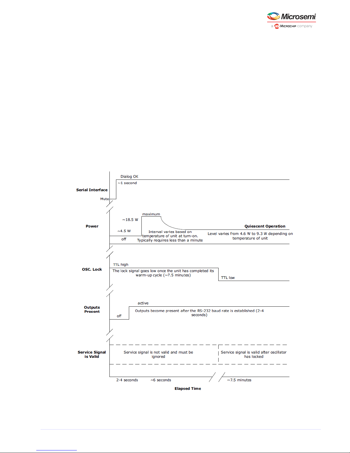
4.2 Start-Up Sequence
When power is connected, the SA.22c begins its warm-up cycle. After few minutes, the rubidium
oscillator reaches a locked condition and its output signals stabilize. The accuracy at shipment is
<±5 × 10 at 25 °C, typical.
–11
Note: Signals appear at the outputs immediately after power is applied to the unit, but these output
signals are not stable until the oscillator is locked.
After 7.5 minutes, the accuracy of the SA.22c oscillator is <1 × 10 . Performance of the SA.22c unit
–9
varies according to the application profile specified at the time of order. For information about
application profiles and unit performance, see the SA.22c Product Specification.
To monitor the performance and selectively of the unit, modify using the MSIP firmware included in the
unit and connect the unit to the COM port of a PC running Windows.
Figure 8 • Sequence of Start-Up Events
Note: The service signal can be active high or active low depending on the unit configuration.
Designer Reference and User Guide Revision D 13
Page 17

SA.22c Rubidium Oscillator
4.3 Theory of Operation
The SA.22c controls the frequency of a quartz crystal oscillator through a frequency-locked loop (FLL)
using the atomic resonance property of rubidium ( Rb).
87
The FLL function block is shown in the following illustration. A microwave signal is derived from a
voltage controlled crystal oscillator (VCXO) and is applied to the Rb vapor within a glass cell. The light
87
of a rubidium lamp passes through this cell and illuminates a photo detector. When the frequency of the
applied RF signal corresponds to the frequency of the ground-state hyperfine transition of the Rb atom
87
(an ultra-stable high-Q rubidium atomic resonance), the light is absorbed causing a change (decrease) in
photo detector current (IPH).
As the change in current is small, modulation techniques are required to extract the desired signal from
the noise background.
The photo detector current generates a control signal with phase and amplitude information, which
permits continuous regulation of the VCXO frequency. The servo section converts the photo detector
current into a voltage, then amplifies, demodulates, and integrates it for high DC servo loop gain.
Figure 9 • Rb Control Loop Block Diagram
4.4 Troubleshooting
After installation, if the SA.22c unit fails to provide outputs, or the rubidium oscillator fails to achieve
lock, check for the following faults:
External power supply is providing incorrect power
I/O connector is defective—perform a continuity check
Note: All pins must have a connection in the I/O connector. This is important for the power and ground
pins.
Operating area has excess humidity or moisture
Ambient temperature is below –10 °C or above 75 °C (the unit may not startup in excessively cold or
hot temperatures)
4.5 Repairs and Support
The SA.22c is not field repairable, but some firmware upgrades can be done in the field, as mentioned in
. If the unit fails, do not remove the cover of the unit and attempt to Start-Up Sequence (see page 13)
make repairs.
Note: Unit warranty is void if the cover is removed or if the protective seals covering the two tuning and
adjustment holes are torn or removed.
Designer Reference and User Guide Revision D 14
Page 18

SA.22c Rubidium Oscillator
4.5.1 Email
Communicate your technical questions to our email address and receive answers back by email:
For USA, Americas, Asia, and Pacific Rim: ftd.support@microsemi.com
For Europe, Middle East, and Africa (EMEA) Technical Support: ftd.emeasupport@microsemi.com
For EMEA Sales: ftd.emea_sales@microsemi.com
4.5.2 Contact
4.5.2.1 USA, Americas, Asia, and Pacific Rim
Microsemi FTD Services and Support
3870 N, First Street
San Jose, CA 95134
Telephone: 408-428-7907
Toll-free in North America: 1-888-367-7966
4.5.2.2 Europe, Middle East, and Africa (EMEA)
Microsemi FTD Services and Support EMEA
Altlaufstrasse 42
Hoehenkirchen-Siegertsbrunn 85635
Germany
Telephone: +49 700 3288 6435
Fax: +49 8102 8961 533
Designer Reference and User Guide Revision D 15
Page 19
SA.22c Rubidium Oscillator
5 Appendix: Using the Developer’s Kit
This appendix provides information about using the SA.22c developer’s kit. It includes information about
interfacing the adapter test board and the various options for providing power and viewing signals from
the SA.22c through the adapter test board.
The SA.22c developer's kit is provided by Microsemi as a design aid and development tool. It allows you
to experiment with the Microsemi SA.22c product in various applications and determine how to
implement it in the most advantageous manner.
The developer's kit contains a hard copy of this document, the SA.22c unit, the adapter test board, an
optional heat sink, application notes, and a CD with electronic files documenting the specifications and
performance of the unit.
Note: Contents of the Developer's Kit may change. Consult the packing list for an up-to-date list of
materials.
Note: Use a power supply with leads or interface cable to connect the adapter test board to the main
power. To avoid potential damage to the adapter test board and the SA.22c, ensure that correct polarity
is used.
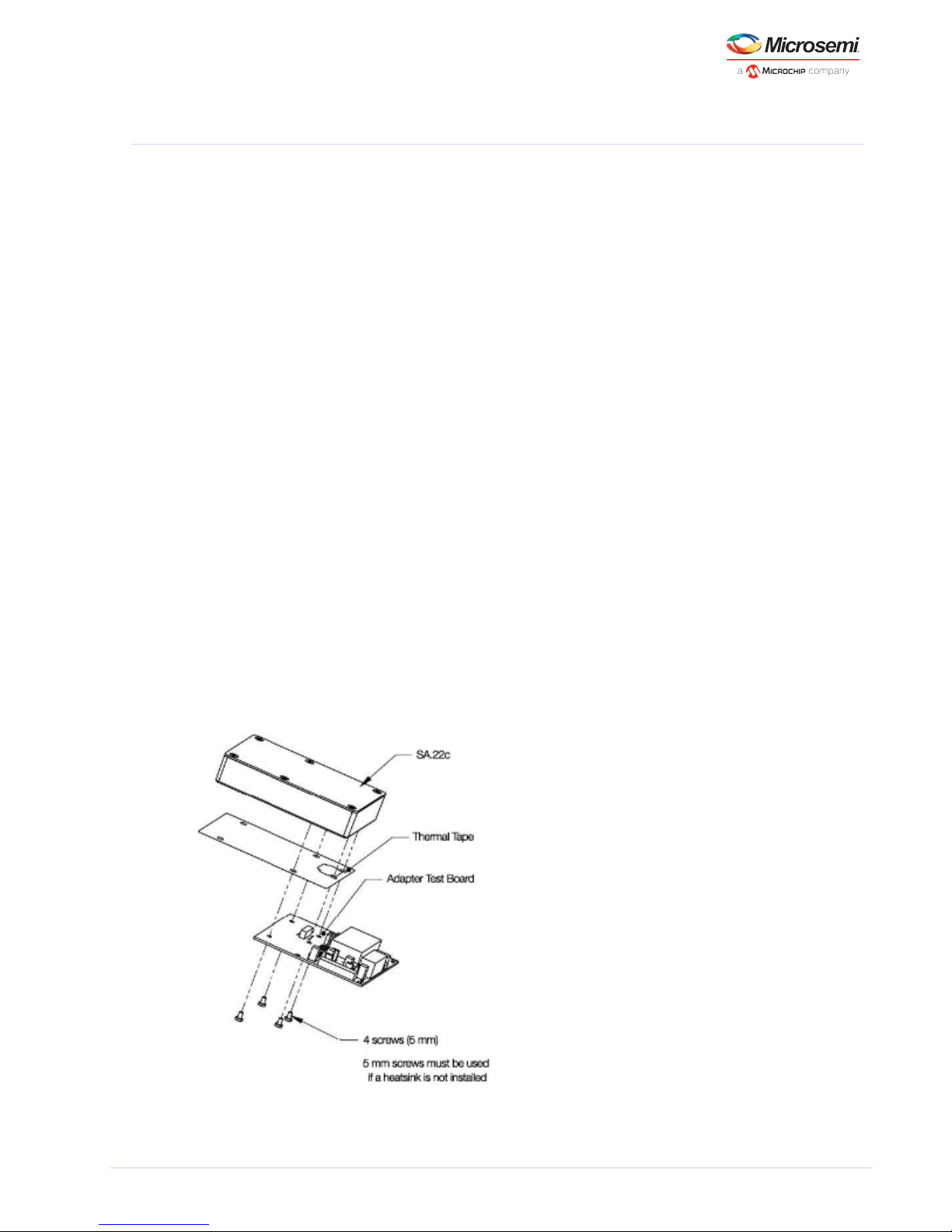
5.1 Mounting the Unit with the Adapter Test Board
The SA.22c, along with the adapter test board, is designed to mount on a heat-absorbing surface. If a
heat-absorbing surface is not available for testing, a suitable heat sink can be ordered as an option.
Note: The mounting screws of the SA.22c are metric (not SAE) and are 3 mm in length with a 0.5 mm
thread pitch. They must not penetrate more than 3 mm into the SA.22c base plate.
The following illustration shows the mounting of the SA.22c on the adapter test board. Four 5 mm
screws are required to mount the SA.22c on the adapter test board if the optional heat sink is not used.
Note: To achieve and maintain the highest level of performance for the SA.22c, Microsemi recommends
utilizing a suitable means for heat sinking if you choose not to purchase the optional heat sink.
Figure 10 • SA.22c Developer’s Kit without Heatsink Assembly
Designer Reference and User Guide Revision D 16
Page 20

SA.22c Rubidium Oscillator
The following figure shows the mounting of the SA.22c on the adapter test board and to the optional
heat sink. Six 10 mm screws are required to properly mount the SA.22c with the adapter test board on
the optional heat sink.
Figure 11 • SA.22c Developer’s Kit with Heatsink Assembly
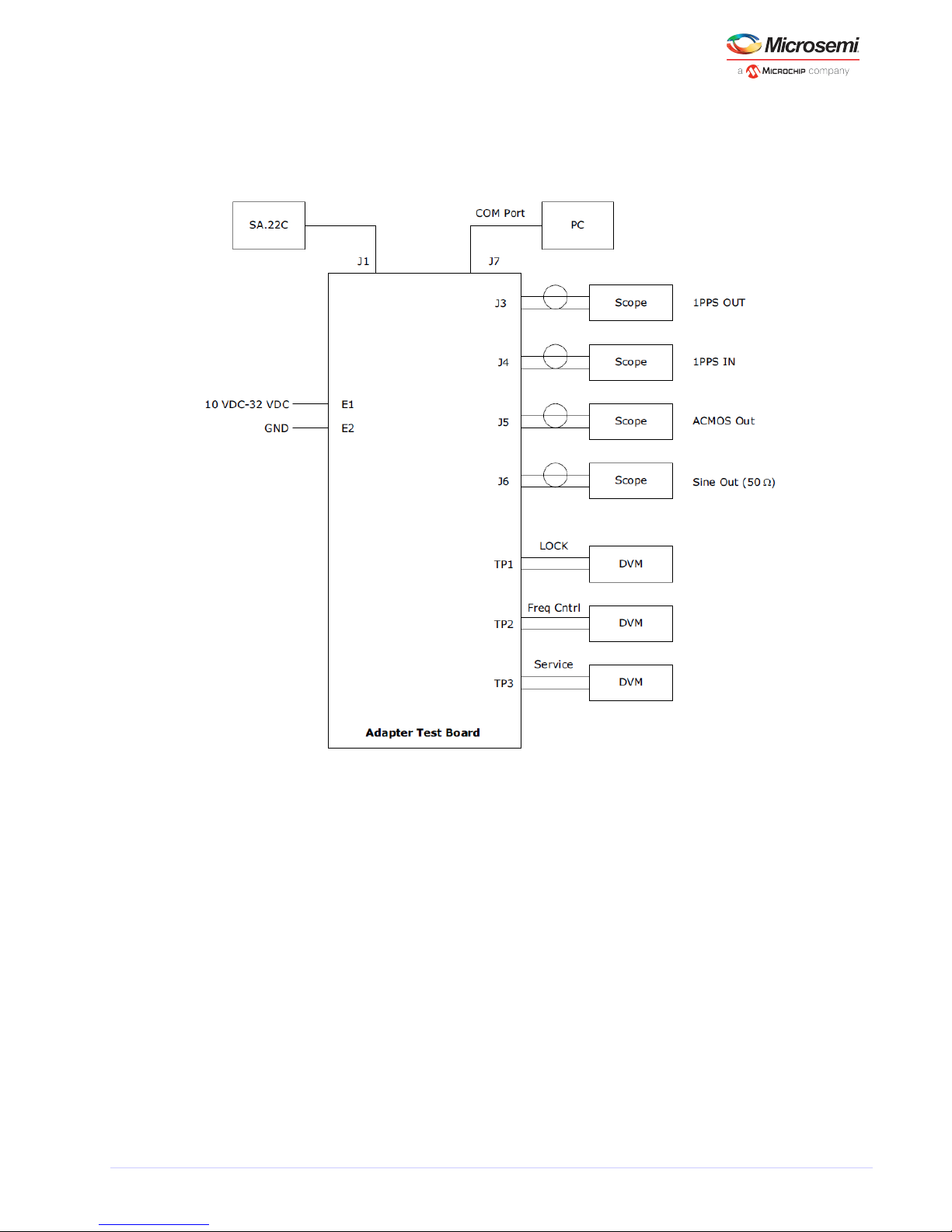
5.2 Interfacing the Adapter Test Board
The adapter test board is designed to deliver power to and retrieve signals from the SA.22c. The adapter
test board allows you to electrically integrate the SA.22cto an existing system (via J2). The following
illustration shows the top view layout of the adapter test board with SA.22c attached.
Figure 12 • Developer’s Kit Interconnect Diagram
J1 on the adapter test board is an 18-pin Samtec 2x9 shrouded I/O header used for electrically
connecting the SA.22c to the adapter test board. The following table lists the I/O pin configuration.
Designer Reference and User Guide Revision D 17
Page 21

SA.22c Rubidium Oscillator
The following table provides information on the pin assignment and the function chart for SA.22c.
Table 5 • 18-Pin Samtec I/O Connector (J1)
Pin Signal Type Function
1 VSS GND Power and signal return ground (all ground pins must be connected)
2 VDD PWR 15 Vdc power input (all power pins must be connected)
3 VSS GND Power and signal return ground (all ground pins must be connected)
4 VDD PWR 15 Vdc power input (all power pins must be connected)
5 FREQ CTRL Analog Frequency control - analog input between 0 - 5 Vdc
6 VCC PWR 5 Vdc power input
7 1PPS OUT Output 1PPS output, may be enabled/disabled digitally
8 VSS GND Power and signal return ground (all ground pins must be connected)
9 FSCMOS Output (FACMOS) ACMOS output (frequency selectable at factory)
10 VSS GND Power and signal return ground (all ground pins must be connected)
11 VSS GND Power and signal return ground (all ground pins must be connected)
12 SERVICE Output Indicates unit is nearing limits of frequency control and that Service is
required within several months.
13 DIN Input UART data in at ACMOS logic levels
14 Lock Output If low, indicates Rb oscillator is locked
15 1PPS IN Input 1PPS input, positive edge triggered
16 DOUT Output UART data out at ACMOS logic levels
17 Not available
18 Not available
J2 is a 26-pin Molex receptacle connector used for delivering power, transmitting/receiving signals, and
data to and from the SA.22c. The following table lists the Molex pin configuration.
Table 6 • 26-Pin Molex Connector (J2)
Pin Signal Type Function
1 VINPUT PWR Power input 10 Vdc to 32 Vdc (All power pins must be connected)
2 VINPUT PWR Power input 10 Vdc to 32 Vdc (All power pins must be connected)
3 VINPUT PWR Power input 10 Vdc to 32 Vdc (All power pins must be connected)
4 VINPUT PWR Power input 10 Vdc to 32 Vdc (All power pins must be connected)
5 VINPUT PWR Power input 10 Vdc to 32 Vdc (All power pins must be connected)
6 VINPUT PWR Power input 10 Vdc to 32 Vdc (All power pins must be connected)
7 VINPUT PWR Power input 10 Vdc to 32 Vdc (All power pins must be connected)
8 SERVICE Output Service required within 30 days based on unit health
9 DOUT Output UART data out at ACMOS logic levels
10 DIN Input UART data in to SA.22c
11 FREQ CTRL Analog Frequency control analog voltage (0 to 5 Vdc)
12 VSS GND Indicates unit is nearing limits of frequency control and that service is
required within months
13 VSS GND Power and signal ground (All ground pins must be connected)
14 VSS GND Power and signal ground (All ground pins must be connected)
Designer Reference and User Guide Revision D 18
Page 22

SA.22c Rubidium Oscillator
Pin Signal Type Function
15 VSS GND Power and signal ground (All ground pins must be connected)
16 VSS GND Power and signal ground (All ground pins must be connected)
17 VSS GND Power and signal ground (All ground pins must be connected)
18 VSS GND Power and signal ground (All ground pins must be connected)
19 1PPS IN Input 1PPS input, positive edge triggered
20 1PPS OUT Output 1PPS output, may be enabled/disabled digitally
21 Lock Output If low, then the SA.22c is locked
22 Not available
23 VSS GND Power and signal ground (All ground pins must be connected)
24 FACMOS Output Frequency ACMOS signal output
25 VSS GND Power and signal ground (All ground pins must be connected)
26 SINE Output Sine signal output (50 ?)
J3, J4, J5, and J6 are SMA connectors used for signal outputs (J4 is a signal input) provided by the SA.22c.
The following table lists the SMA connectors' signal information.
Table 7 • SMA Connectors' Signal Information
SMA Signal Type Function
J3 1PPS OUT Output 1PPS output, may be enabled
/disabled digitally
J4 1PPS IN Input 1PPS input, positive edge triggered
J5 FACMOS Output Frequency ACMOS signal output
J6 SINE Output Sine signal output (50 Ω)
J7 is a 9-pin D-Sub connector used for transmitting/receiving data to and from the SA.22c through the
MSIP. The following table lists the D-Sub connector pin configuration.
Warning: When using J3, J4, J5, and J6, it is required that J2 must not be connected. Having J2 connected
will cause a loading effect on J3, J4, J5, and J6, which results in degraded signal integrity.
Table 8 • 9 Pin D-Sub Connector (J7)
Pin Signal Type Function
1 Not available
2 DOUT Output UART data out at ACMOS logic levels
3 DIN Input UART data in to SA.22c
4 Not available
5 VSS GND Signal ground
6 Not available
7 Not available
8 Not available
9 Not available
5.3 Options for Supplying Power to the Adapter Test Board
The SA.22c adapter test board design allows three power-supplying options.
Designer Reference and User Guide Revision D 19
Page 23
SA.22c Rubidium Oscillator
The following figures show the block diagrams of the three different options for powering and setting up
the SA.22c with the adapter board. It also shows the connections used to access various inputs and
outputs of the SA.22c depending on the option selected.
Figure 13 • Block Diagram of Suggested Test SA.22C Set-up (Option 1)
After the SA.22c unit receives power, wait for a few minutes while the unit achieves atomic lock. During
this period, the monitored lock signal must be HIGH. After the unit achieves atomic lock, the lock signal
goes LOW.
Designer Reference and User Guide Revision D 20
Page 24

SA.22c Rubidium Oscillator
Figure 14 • Block Diagram of Suggested Test SA.22C Set-up (Option 2)
It is recommended to power up 5 V first, or simultaneous with the 15 V supply.
After the SA.22c unit receives power, wait for a few minutes while the unit achieves atomic lock. During
this period, the monitored lock signal should be HIGH. After the unit achieves atomic lock, the lock
signal goes LOW.
Designer Reference and User Guide Revision D 21
Page 25

SA.22c Rubidium Oscillator
Figure 15 • Block Diagram of Suggested Test SA.22C Set-up (Option 3)
After the SA.22c unit receives power, wait for few a minutes while the unit achieves atomic lock. During
this period, the monitored lock signal must be HIGH. After the unit achieves atomic lock, the lock signal
goes LOW.
The following figure shows the physical power supply wiring and jumper settings needed for each
option.
Warning: Use the power settings and connectors that are appropriate for one particular option at a
time. Mixing any combination of these options may result in system failure and may cause damage to
the existing circuitry.
Designer Reference and User Guide Revision D 22
Page 26

SA.22c Rubidium Oscillator
Figure 16 • Power Supply and Output Options
Designer Reference and User Guide Revision D 23
Page 27

SA.22c Rubidium Oscillator
Option 1 allows you to directly power the adapter test board with 10 Vdc to 32 Vdc supplied to E1 and
E2 connected to supply ground. TB1 is installed and TB2 and TB3 are open. In the adapter board, this
voltage travels through a DC-to-DC converter and a voltage regulator to supply the SA.22c with 15 Vdc
and 5 Vdc for operation. For this option, J7 is used for serial interface communications, J3, J5, and J6 are
used for signal outputs, and J4 is used for 1PPS input. TP1 and TP3 are used for lock and service monitor
respectively. TP2 is used for providing the analog frequency control if needed. In this option, J2 must not
be connected to avoid degraded signal integrity.
Option 2 allows you to directly power the adapter test board with separate 15 Vdc supplied to E5 and
5 Vdc supplied to E3 supplies with E4 connected to supply ground. TB2 and TB3 are installed and TB1 is
left open. In the adapter board, these voltages travel directly to the SA.22c for operation (the 5 Vdc
must be applied before or simultaneous to the 15 Vdc). For this option, J7 is used for serial interface
communications, J3, J5, and J6 are used for signal outputs, and J4 is used for 1PPS input. TP1 and TP3
are used for lock and service monitor respectively and TP2 is used for providing the analog frequency
control if needed. In this option, J2 must not be connected to avoid degraded signal integrity.
Option 3 allows you to power the adapter test board with 10 Vdc to 32 Vdc through the 26-pin Molex
connector (J2). TB1 is installed and TB2 and TB3 are open. In the adapter board, this voltage travels
through a DC-to-DC converter and a voltage regulator to supply the SA.22c with 15 Vdc and 5 Vdc for
operation. For this option, J7 or J2 is used for serial interface communications, J2 is also used for input
and output signals. TP1 and TP3 are used for lock and service monitor respectively and TP2 is used for
providing the analog frequency control if needed; however, J2 can also provide these monitors and
frequency control as well (see for Molex pin configuration). 26-Pin Molex Connector (J2) (see page 18)
In this option, J3, J4, J5, and J6 must not be connected to avoid degraded signal integrity.
Designer Reference and User Guide Revision D 24
Page 28

SA.22c Rubidium Oscillator
6 Appendix: Microsemi Serial Interface Protocol
This appendix provides information about communicating with the SA.22c through the serial interface
connector provided in the developer’s kit (see ). It Appendix: Using the Developer’s Kit (see page 16)
includes output examples and a description of commands.
6.1 Using the Microsemi Serial Interface Protocol
The MSIP bridges communication with the SA.22c through the serial port when connected to a host PC.
All commands are a single ASCII letter and require no termination. Out of the eight developer-mode
RUN MODE commands, three require the host to supply data.
6.1.1 Host Terminal Emulator Setup
Set up the comm port of the PC with the following configuration:
Data rate (baud or B.P.S. – baud rate) of the SA.22c is 57.6K
No parity
Eight data bits
One stop bit
No local echo (unit echoes)
No hardware or software flow control
Note: The SA.22c’s UART connections are based on 5 Vdc logic levels. However, the developer’s kit
contains a TTL-to-RS232 converter that allows interfacing to a PC.
6.1.2 Run Mode Data Format (Customer Mode)
SA.22c outputs are all decimal data as ASCII coded hex except for the echoed characters. Do not convert
data to decimal when transmitting to the SA.22c. All data are sent to the SA.22c and received back as
. The following example shows how data are encoded.ASCII coded hex
Note: Flow control is not permitted in .Run Mode
The following is an example of the output from the SA.22c after power is supplied to the unit.
SA22C by Symmetricom, Inc., Copyright 2006
SA22 Version 6.01C of 7/2006; Loader Version 3
Mode CN01 Flag 0000 [D04D]ok
Unit serial code is 0612SA3763-h, current tuning state is 6
Crystal: 60000000hz, ACMOS: 10000000.0hz, Sine: 10000000.0hz
Ctl Reg: 004C, Res temp off: -1.5410, Lamp temp off: -1.9466
FC: disabled, Srvc: high
Enter Run Mode
FC mode is disabled
1pps mode is disabled
r>
Command i: The following example shows the response to the command i to get the serial number and
other information on the SA.22c:
r>i
SA22C by Symmetricom, Inc., Copyright 2006
SA22 Version 6.01C of 7/2006; Loader Version 3
Mode CN01 Flag 0004
Unit serial code is 0612SA3763-h, current tuning state is 6
Crystal: 3938700hz, ACMOS: 989680.00000000hz, Sine:
Designer Reference and User Guide Revision D 25
Page 29

SA.22c Rubidium Oscillator
989680.00000000hz
Ctl Reg: 004C, Res temp off: BFC53F7D., Lamp temp off: BFF92B93.
FC: disabled, Srvc: high
Command h: The following example shows the response to the command h for the SA.22c help menu:
r>h
a: Set FC Mode
f: Adjust DDS Frequency (delta e-11)
i: Info (show program info)
j: Display 1pps Delta Reg
k: Set 1pps TIC
l: Set Service Pin Sense
o: Set ACMOS Output Frequency 'N'
p: Display Control Reg
q: Set Control Reg
t: Save Tuning Data
w: Display Health Data
x: Exit Run Mode
r>
Command w: The following example shows the response to the command w for the SA.22c health data
(wellness):
r>w
AData:
SCont: 6012
SerNum: 3B8
PwrHrs: 8A
PwrTicks: E291DB
LHHrs: 85
LHTicks: 16CCE28
RHHrs: 85
RHTicks: 165353C
dMP17: 4156AE53.
dMP5: 3D3C8652.
dHtrVolt: 41852146.
PLmp: 3F7E1248.
Appendix: Microsemi Serial Interface Protocol
097-16313-201 Designer Reference and User Guide Revision B 29
PRes: 3FC3EE0D.
dLVthermC: B8530000.
dRVthermC: B9384000.
dLVolt: 3FA0E4AC.
dMVoutC: C87BD20F.
dTempLo: 412C0000.
dTempHi: 42B50000.
dVoltLo: 416156C8.
dVoltHi: 4185C42A.
iFpgaCtl: 004C
dCurTemp: 42540000.
dLVoutC: 3DF9793A.
dRVoutC: 3DE6A30F.
dMV2demAvg: 3F259383.
Note: Values are in hex format.
Designer Reference and User Guide Revision D 26
Page 30

SA.22c Rubidium Oscillator
Command a: The following example shows the response to the command a followed by an integer sets
the enable/ disable feature of FC mode. Integer zero followed by <cr> disables FC mode and any
nonzero integer followed by <cr> enables the FC mode.
r>a
5987717
FC mode enabled
Command p: The following example shows the response to the command p for the SA.22c control
register
r>p
Control Reg: 204C
Note: For the above example, C corresponds to bits 12-15, 4 corresponds to bits 8-11, 0 corresponds to
bits 4-7, and 2 corresponds to bits 0-3 in the following table.
Table 9 • SA-22c (and x72) Output Control Register
Bit Hex
Value
Control Description Controlled By
0 1 Lamp
switch
power
boost—
internal
function
0= Lamp switch off (default during
operation)
1= Lamp switch on
Controlled by SDCP, automated function, no user input
1 2 BITE
output
0= Unit is locked (default during
operation)
1= Unit is not locked
Controlled by SDCP-automated function- no user input
2 4 FXO
(crystal
output)
enable
0= Enables FXO output
1= Disables FXO output
Configuration is set either by entering the control register value
during TACO or entering the configuration information into the unit
batch list file prior to testing
3 8 1PPS
output
enable
0= Enables 1PPS output
1 =Disables 1PPS output
Configuration is set either by entering the control register value
during TACO or entering the configuration information into the unit
batch list file prior to testing
4 1 ACMOS
output
enable
0= Enables ACMOS output
1= Disables ACMOS output
Configuration is set either by entering the control register value
during TACO or entering the configuration information into the unit
batch list file prior to testing
5 2 C-field
boost
0= Low C-field (default)
1= High C-field
Configuration is set by entering the control register value during
TACO. Not configurable in customer firmware
6 4 Sine
output
enable
0= Enables sine output to 40% of
max amplitude
1= Disables sine output
Configuration is set either by entering the control register value
during TACO or entering the configuration information into the unit
batch list file prior to testing
7 8 Sine
output
level
adjust
0= Zero additional level (default)
1= Adds 15% of max output
Configuration is set by entering the control register value during
TACO. Not configurable in customer firmware.
8 1 Sine
output
level
adjust
0= Zero additional level (default)
1= Adds 10% of max output
Configuration is set by entering the control register value during
TACO. Not configurable in customer firmware.
Designer Reference and User Guide Revision D 27
Page 31

SA.22c Rubidium Oscillator
Bit Hex
Value
Control Description Controlled By
9 2 Sine
output
level
adjust
0= Zero additional level
1= Adds 5% of max output
(default)
Configuration is set by entering the control register value during
TACO. Not configurable in customer firmware.
10 4 Service 0= Unit is OK
1= Unit requires service
Controlled by SDCP, automated function, no user input
11 8 1PPS
locked
(sync)
0= No 1PPS sync
1= 1PPS locked to ext 1PPS
Controlled by SDCP, automated function, no user input
12 1 External
1PPS
0= No 1PPS external signal
1= 1PPS external signal present
Controlled by SDCP, automated function, no user input
13 2 FC pin
enabled
0= Frequency control pin disabled
1= Frequency control pin enabled
Controlled by SDCP, automated function, no user input
14 4 Reserved
not used
15 8 Reserved
not used
6.1.3 Factory Mode
Data output from the SA.22c in factory mode is not intended for users outside the factory and is not
described in this document beyond the table .Run Mode Commands (see page 28)
Caution: Using factory mode results in the erasure of firmware on the SA.22c rendering it inoperable
and making it necessary to return the unit to the factory for re-programming.
6.1.4 Serial Interface Initialization
The serial interface is initialized as listed in the following tables.
Table 10 • Run Mode Commands
User Output
to SA.22c
Response to
Host
Command Name and Description
a Set FC mode
Example: a <zero or
non-zero integer>
<cr>
To be specified Set analog frequency control mode.
This command toggles the analog input pin to the unit between enable and Freq Cntrl
disable. In factory mode, the default is enabled. During factory test, the default is set
to disable for shipping unless the customer ordered the default to be set enabled.
f Desired frequency
change from free
running center
frequency in parts to
1×10
–11
Example: for a
100×10
–11
change: 100<cr>
Example: for a –
100×10
–11
change: –100<cr>
To be specified Adjust frequency.
Adjust unit output frequency. Used to discipline the unit. The smallest incremental
frequency change is 2×10 (or ). Any value less than this will still be allowed, but
–12
f.2
not executed by the hardware. Maximum value that can be used at one time is 4×10 .
–8
For larger frequency changes, repeated steps equal to or smaller than 4×10 must be
–8
used. Unit always powers up at free running factory set frequency. This command is
always relative to the free running frequency.
h To be specified Help command.
Displays menu.
i To be specified Outputs unit information.
While dumping data, clock outputs are not guaranteed to meet specifications during
the use of this command.
Designer Reference and User Guide Revision D 28
Page 32

SA.22c Rubidium Oscillator
1.
2.
User Output
to SA.22c
Response to
Host
Command Name and Description
o N (example of
command and data to
give 10 MHz for a
VCXO of 60 MHz is:
)o3
To be specified The default frequency output is 10 MHz .
1
p To be specified Displays control register.
q Hex data to set or
reset bits in the control
register
immediately follows
the command
(Example: )q3A
To be specified Set control register
Allows enabling or disabling of outputs.
t SAVE command
Example: to SAVE
changes:
5987717<cr>
To be specified Saves all changes made .
2
w To be specified Displays health monitor data.
Contact the manufacturer for information about other frequencies.
If the t command is not used, unit defaults to factory settings at next power up.
Table 11 • Factory Mode Commands
User Output to SA.22c Response to Host Command Name and
Description
Command Data
a a> Goes to administration mode.
i Outputs 7 lines of banner (same as power-up information) Displays unit Information.
r Run
mode
Enter run mode. FC mode is disabled (enabled) Goes to run mode.
Note: Run mode and admin mode allow the loading of new code, updates, or reconfiguring defaults in
the field. It is not a normal operating mode.
Table 12 • SA.22c Administrative Mode Commands
User Output to SA.22c Response to Host Command Name and Description
Command Data
a Outputs 7 lines of banner
(same as power-up
information)
Unit information same as the i command in factory
mode and run mode.
b File from
Microsemi (selfburning)
To be specified Operating this command without valid file will not
overwrite the existing data stored in flash memory.
x Run mode x f> Exit administrative mode to factory mode.
y Y asks are you sure? Soft reset. Restarts processor.
z Z asks are you sure? Puts unit into a mode where it will wake only when
the power is recycled.
Note: Admin mode allows the loading of new code, updates, or reconfiguring defaults in the field. It is
not a normal operating mode.
Designer Reference and User Guide Revision D 29
Page 33

SA.22c Rubidium Oscillator
7 Appendix: One Pulse Per Second Source Connection
This appendix describes how to connect a 1PPS source, such as a commercial GPS receiver, to an SA.22c
to achieve long term accuracy and excellent holdover, or flywheeling performance.
7.1 Connection Requirements
The following connections are required for 1PPS setup:
Power
GPS antenna/receiver or other 1PPS source reference.
1PPS cabling from the source to the SA.22c
No serial port communication is required for initial setup unless the changes are made from the factory
default settings. Information on setup, operation, and integration is provided.
7.2 Background
GPS technology has made time and frequency synchronization possible (available) worldwide.
Connecting the 1PPS output from a commercial (civilian) GPS receiver to an SA.22c provides a cost
effective system that maintains highly accurate time and frequency even when GPS signals are
unavailable, for example, during jamming and antenna maintenance.
The GPS system provides 1PPS signals worldwide with good long term stability (that is, <1×10
–12
averaged over 24 hours). However, the short term stability of this signal is often compromised by
various noise sources, for example, man-made, atmospheric conditions, crosstalk, RF multi-path or inter
symbol interference, and GPS receiver oscillator limitations.
Microsemi has pioneered the use of rubidium oscillators in telecommunication applications.
Telecommunications applications require long term and short term stability beyond the range of free
running quartz oscillators. For example, cellular CDMA systems require 1PPS signals to be synchronized
within 2 μs over long periods of time even when GPS signals are not available. To achieve this
performance, system designers must combine the benefits of short term stability (from a rubidium or
low noise OCXO) with long term stability (from GPS, Loran-C, Glonass, or Cesium). Microsemi is the
leader in system products with microprocessor driven circuitry that uses the GPS 1PPS system to steer
various oscillators (Cesium, Rubidium, and Quartz). These products make it possible to combine the
short term with long term stability. With SA.22c, the solution is more cost effective. The performance
level of SA.22c used with a GPS receiver approaches the performance of Cesium oscillators used in
telecommunication systems.
7.3 1PPS Functions
The SA.22c can be configured to:
Generate a rubidium controlled 1PPS signal
Measure the difference between an incoming 1PPS signal and the SA.22c 1PPS
Synchronize the SA.22c’s frequency and 1PPS output to the incoming 1PPS and provide long
holdover times
The following figure shows the SA.22c 1PPS disciplining block diagram.
When an externally generated 1PPS signal is applied to the 1PPS input pin of a properly configured SA.
22c, the unit provides the time interval error difference between the 1PPS input and the 1PPS generated
inside the SA.22c (see table ). The difference is 1PPS States Returned with the j Command (see page 33)
read using the RS232 communications j command. The j command displays the difference between the
1PPS input and the 1PPS generated internally by the SA.22c. The j command generates a number
representing the number of TICS in a delta register. If the SA.22c has a 60 MHz crystal, each TIC is 16.7
ns (1.67×10 ). This number is in hex format.
–8
Designer Reference and User Guide Revision D 30
Page 34

SA.22c Rubidium Oscillator
The test bench setup configuration allows the SA.22c to be disciplined by the incoming 1PPS signal. The
following figure Test Bench Setup shows the test bench setup. The 1PPS disciplining mode is enabled by
default. It can be temporarily disabled by issuing the g command followed by a 1 (see The g Command
). Typical performance data for this configuration is shown in (see page 34) Flywheeling Recover with
and .1PPS offset <1 μsec (see page 35) Flywheeling Recover with 1PPS offset >1 μsec (see page 36)
Figure 17 • Time and Frequency Control System
Figure 18 • Test Bench Setup
7.4 System Requirements
The following are the requirements for 1PPS setup and operation:
SA.22c with 1PPS output enabled
GPS receiver with less than 300 ns noise
Designer Reference and User Guide Revision D 31
Page 35

SA.22c Rubidium Oscillator
1.
2.
3.
1PPS input signals must have repeatable rise time with minimal ringing and must conform to the
following:
1PPS input is driven by a standard 3.3 V logic, 5 V CMOS, or 5 V TTL with normal operation at:
Input voltage logic high: 2.00 V minimum
Input voltage logic high: 5.50 V maximum
Input voltage logic low: 0.00 V minimum
Input voltage logic low: 0.80 V maximum
Maximum DC overshoot must be limited to 5.5 V or 10 mA, whichever is easiest to achieve.
Maximum DC undershoot must be limited to –0.5 V or 10 mA, whichever is easiest to achieve.
Minimum pulse width (or hold time) of 50 ns.
Input impedance >100 KΩ allows you to terminate the 1PPS at the input to the SA.22c with 50 Ω
at the SA.22c input pin or drive the SA.22c high impedance directly with a low impedance source
such as 50 Ω or any ACMOS gate as long as the input voltage level at the SA.22c pin is met as
described above.
The SA.22c rubidium oscillator subsystem must be locked to achieve synchronization.
The SA.22c must be set up with the proper time constant and damping factor.
SA.22c adapter kit is recommended to facilitate setup.
PC running Microsoft Windows with terminal emulation program. (57600 bps, 8 bits with no parity).
7.5 1PPS Algorithm Operation
There are two parameters that are modified by the user for 1PPS synchronization using the command y
– damping factor and tau.
Damping factor—determines the relative response time and ringing in response to each step. Values
must be between 0.25 and 4. Values less than 0.25 defaults to 0.25 while values over 4 defaults to 4.
Tau (or time constant)—expressed in seconds and determines the time constant of the PLL for following
a step in phase for the reference. The range of tau is 5 to 100,000 seconds. Values outside this range
cause both the damping factor and tau to change to the factory default settings.
7.5.1 Factory Default
The factory default requires no inputs to the rubidium oscillator. The default value for damping factor is
1 and the default value for tau is 400. These values are a good starting points and work well for most
GPS applications.
7.6 Setting the 1PPS Synchronization
The following are the steps for setting 1PPS signal synchronization (SA.22c with 1PPS enabled customer
version of firmware at revision 6.05c or higher installed.)
Connect the SA.22c to the adapter test board of the developer’s kit or to a correctly configured
equivalent system. (see )Appendix: Using the Developer’s Kit (see page 16)
Ensure that the terminal emulation program is configured to 57,600 BPS, 8 bits, no parity, no flow
control, and the keyboard caps lock is off. All inputs must be in lower case.
Power up the system. The header information from the SA.22c is displayed as follows, where the
firmware version needs to be confirmed.
SA22C by Symmetricom, Inc., Copyright 2006
SA22 Version 6.05C of 7/2006; Loader Version 3
Mode CN03 Flag 0000 [C91F]ok
Unit serial code is 0612SA3763-h, current tuning state is 6
Crystal: 60000000hz, ACMOS: 10000000.0hz, Sine: 10000000.0hz
097-16313-201 Designer Reference and User Guide Revision B 36
Ctl Reg: 0044, Res temp off: -1.5410, Lamp temp off: -1.9466
FC: enabled, Srvc: low
Enter Run Mode
FC mode is enabled
Designer Reference and User Guide Revision D 32
Page 36

SA.22c Rubidium Oscillator
1.
2.
3.
4.
5.
1pps mode is enabled
r>
Note: It is not necessary for the SA.22c to be locked to enter the 1PPS configuration commands, but it
must be locked for actual synchronization to occur.
7.6.1 Changing the y Coefficients
Follow the steps to change the y coefficients
At the r> prompt, type y, then 1, and press Enter (1 indicates that the damping factor needs to be
entered).
Enter a value between 0.25 and 4, and press Enter (see Note 3 in The g Command (see page 34)
and ).1PPS Algorithm Theory of Operation (see page 36)
At the r> prompt, type y, then 2, and press Enter (2 indicates that the time constant needs to be
entered).
Enter a value between 5 and 100000, and press Enter (see Note 3 in The g Command (see page 34)
and ).1PPS Algorithm Theory of Operation (see page 36)
At the r> prompt, type z. This saves the 1PPS configuration data to non-volatile memory. If the y
coefficients are not saved with the z command, the SA.22c reverts to the previously saved
configuration upon restart. The SA.22c responds with the following output (see Note 9 in The g
):Command (see page 34)
r>z
Saving TData 2, serial number 3BE
1pps Coefs saved
7.6.2 The y Coefficients – Factory Default
If the factory default values of damping factor = 1 and tau = 400 are acceptable for the application, no
modifications to the y coefficients are required. The SA.22c 1PPS disciplining is enabled at the factory,
which allows the unit to work right out of the box. If the y coefficients need to be restored to the factory
defaults, enter the value 0 for both the damping factor and tau using the process described in Changing
. The SA.22c operates at the factory default damping factor of 1 and tau the y Coefficients (see page 33)
of 400.
7.6.3 The j Command
Press the j key at any time to return the current value in hex format from the delta register (see Note 1
in ) and the 1PPS state (see Note 2 in The g Command (see page 34) The g Command (see page 34)
and the following table). The following is the output format:
r>j
1pps Delta Reg: 0 ppsState:3
r>.
Table 13 • 1PPS States Returned with the j Command
PPS State Value Action Performed by SA.22c
INITIALIZE0STATE 0 Start up initialization
INITIALIZE1STATE 1 Start up initialization
INITIALIZE2STATE 2 Start up initialization
HOLDOVERSTATE 3 Seeking usable 1PPS
JAMSYNC1STATE 4 Sync SA.22c output 1PPS to input
JAMSYNC2STATE 5 Sync SA.22c output 1PPS to input
DISCIPLINESTATE 6 Keep SA.22c output 1PPS aligned to input by controlling
SA.22c frequency
PIDCALCSTATE 7 Calculations for disciplining algorithm
Designer Reference and User Guide Revision D 33
Page 37

SA.22c Rubidium Oscillator
PPS State Value Action Performed by SA.22c
PDATEDDSSTATE 8 Update SA.22c DDS based on PIDCALCSTATE output
ALCSLOPESTATE 9 Calculate slope of incoming 1PPS vs. SA.22c 1PPS during holdover
For more information on 1PPS states, see .1PPS Algorithm Theory of Operation (see page 36)
7.6.4 The g Command
The g command helps to toggle the operation of the SA.22c in any of the three modes mentioned
below, which affect the output of the lock pin (pin 14 see Note 10 in ). The g Command (see page 34)
This 1PPS mode can be changed but cannot be saved. If power is cycled to the unit, it reverts to the
factory default. The following are the modes of operation:
0 = 1PPS disciplining disabled—Normal rubidium lock pin functionality. Only the rubidium loop
needs to be locked to indicate a locked condition on pin 14.
1 = 1PPS disciplining enabled—Normal lock pin functionality. Only the rubidium loop needs to be
locked to indicate a locked condition on pin 14.
2 = 1PPS disciplining enabled—Requires both rubidium loop to be locked and 1PPS synchronization
lock to indicate a locked condition on pin 14.
There are two types of 1PPS customer firmware. The 1PPS standard firmware provides an Rb or Rb/1PPS
lock indicator at pin 14 and a service indicator on pin 12 of the SA.22c I/O connector. The 1PPS LED
firmware uses the same functions for pin 14, but pin 12 is reserved for 1PPS lock indication only. There
is no service pin on the 1PPS LED versions. The factory default modes set by the g command for each
firmware version are:
1PPS standard firmware—Mode 2. Rb lock and 1PPS lock indicated on pin 14.
1PPS LED firmware—Mode 1. Rb lock only indicated on pin 14 and 1PPS lock indicated on pin 12.
The key sequence to change the output/lock indicator mode with the g command is as follows:
At the r> prompt, type g, then type either 0, 1, or 2 depending on the desired output mode, and press
Enter.
Note: 1 These numbers are in HEX format.
Note: 2 1PPS states: 0 to 2—Initialize; 3, 9—Holdover; 6 to 8—Disciplining.
Note: 3 When connecting to a GPS receiver, the factory default mode is recommended. Start with y1=1
(DF) and Y2=400 TC in seconds). These values work well for most GPS receivers.
Note: 4 Use z command to save your settings.
Note: 5 SA.22c Rubidium system locks approximately 5 minutes after startup.
Note: 6 SA.22c initial frequency must be less than ±3PPB for 1PPS to lock.
Note: 7 Initial 1PPS lock occurs between 3 and 5 minutes after both lock and valid 1PPS are present.
Note: 8 Confirm the firmware version by issuing the i command.
Note: 9 xx is a value returned, which is the hex equivalent of the number of times the table has been
written to. TData can be either 1 or 2.
Note: 10 If the J2 Molex connector is used on the adapter test board, then the lock pin is 21 and the
service pin is 8.
Note: 11 If the lock and service voltages are measured on the adapter test board, then the lock signal is
on TP1 and the service signal is on TP3.
Designer Reference and User Guide Revision D 34
Page 38

SA.22c Rubidium Oscillator
Table 14 • 1PPS Firmware Versions
Version Description
FW6.05c Pin12 provides service indication
FW6.06c Pin12 is reserved for 1PPS lock indication only
7.7 Flywheeling Recovery Example–Normal
In this test, the SA.22c is synchronized to 1PPS before the following data set as shown in the following
figure. Antenna is removed at 0 hour and reapplied at approximately 12.5 hours. The SA.22c 1PPS
output signal reaches an offset of 220 ns.
The subsequent frequency change returns the 1PPS offset to 0 ns.
Figure 19 • Flywheeling Recover with 1PPS offset <1 μsec
Designer Reference and User Guide Revision D 35
Page 39

SA.22c Rubidium Oscillator
7.8 Recovery with JamSynch
In this test, the antenna to the GPS receiver is removed. The SA.22c is set to an off frequency long
enough to induce a 1PPS error over 1 μsec. When the antenna is reapplied, the SA.22c 1PPS recovers by
resetting to 1PPS 0 ns (JamSynch). This procedure is repeated to cause both a leading and lagging 1PPS.
Note: This test is performed on a unit started cold that causes the general curve in the frequency data
(excluding the intentional offsets).
Figure 20 • Flywheeling Recover with 1PPS offset >1 μsec
7.9 1PPS Algorithm Theory of Operation
SA.22c qualifies 1PPS inputs by analyzing the time difference between the SA.22c’s 1PPS output and the
external 1PPS input. This is referred to as the holdover state. The SA.22c determines whether the 1PPS
input is usable by calculating the rate of change in timing measurements that are taken once per
second.
After a 1PPS input is qualified, the SA.22c 1PPS algorithm determines if it is necessary to adjust the
counter that produces the 1PPS output (JamSynch state). The algorithm then begins to adjust the output
frequency of the SA.22c to keep the 1PPS output aligned with the 1PPS input. This is the disciplining
state, and the control method is a proportional integral derivatives (PID) scheme.
The amount of frequency change and the length of time required to reach 1PPS accuracy is adjusted by
setting y1 (damping factor) and y2 (time constant) parameters. During this disciplining state, the timing
of each 1PPS input is compared to the expected value. If the offset exceeds 333 ns, the algorithm
changes to the holdover state and the process begins again. The following figures provide a detailed
explanation.
Designer Reference and User Guide Revision D 36
Page 40

SA.22c Rubidium Oscillator
7.9.1 1PPS Algorithm High Level Flow Chart
The following flow chart explains the 1PPS steer algorithm.
Figure 21 • SA.22c 1PPS Algorithm States
Designer Reference and User Guide Revision D 37
Page 41

SA.22c Rubidium Oscillator
7.9.2 Initialization
During initialization, the algorithm sets up variables based on the time constant (TC) and damping factor
(DF). The SA.22c checks for 1PPS input once per second, and if present, it enters the holdover state.
Automatic mode is used when the time constant is set to 0. The SA.22c 1PPS is in the initialization state
when no 1PPS is applied. The j command shows the 1PPS count.
Figure 22 • SA.22c Initialize State
Designer Reference and User Guide Revision D 38
Page 42

SA.22c Rubidium Oscillator
7.9.3 Holdover
During holdover, 1PPS input statistics are accumulated and the results are calculated periodically
(CalcSlope State). The sample size is set to 120 data points (120 s).
Figure 23 • SA.22c Holdover State
Designer Reference and User Guide Revision D 39
Page 43

SA.22c Rubidium Oscillator
7.9.4 Calcslope
The frequency difference between the SA.22c and the 1PPS source is calculated, and if the difference is
<±3 × 10 , the state changes from holdover to JamSynch. This state executes every 120 s during
–9
holdover.
Figure 24 • SA.22c Calcslope State
Designer Reference and User Guide Revision D 40
Page 44

SA.22c Rubidium Oscillator
7.9.5 JamSynch
The SA.22c 1PPS output is compared to the SA.22c 1PPS input, and if the difference is ≥1 μs, the state
returns to holdover to collect a second data set. When two consecutive slopes are in range, the SA.22c’s
1PPS output is synchronized to its 1PPS input. If the difference is <1 μs, the algorithm waits six more
pulses and then advances to the discipline state.
Figure 25 • SA.22c JamSynch State
Designer Reference and User Guide Revision D 41
Page 45

SA.22c Rubidium Oscillator
7.9.6 Discipline
In the discipline state, the SA.22c uses a proportional-integral-derivative (PID) method to steer the 1PPS
output. The SA.22c average frequency offset is close to zero. There is some frequency change when
recovering from holdover. If at any time a 1PPS input signal is more than 330 ns from its expected value,
the 1PPS algorithm returns to holdover state. If the input source is stable, the SA.22c further refines the
input estimate to provide a smoother frequency output. Every minute the SA.22c saves the DDS setting
in case holdover occurs. Some receivers take a long time to produce 330 ns of error after signal loss; the
SA.22c reverts to the DDS value from two periods before the 1PPS becomes invalid.
Figure 26 • SA.22c Discipline State
Designer Reference and User Guide Revision D 42
Page 46

SA.22c Rubidium Oscillator
Microsemi Headquarters
One Enterprise, Aliso Viejo,
CA 92656 USA
Within the USA: +1 (800) 713-4113
Outside the USA: +1 (949) 380-6100
Sales: +1 (949) 380-6136
Fax: +1 (949) 215-4996
Email: sales.support@microsemi.com
www.microsemi.com
© 2016–2018 Microsemi. All rights reserved. Microsemi and the Microsemi
logo are trademarks of Microsemi Corporation. All other trademarks and
service marks are the property of their respective owners.
Microsemi makes no warranty, representation, or guarantee regarding the information contained herein or the suitability of its products and s ervices
for any particular purpose, nor does Microsemi assume a ny liability whatsoever arising out of the app lication or use of any product or circuit. The
products sold hereunder and an y other products sold by Microsemi have been s ubject to limited testing and should not be us ed in conjunction with
mission-critical equipment or applications. Any performance specifications are believed to be reliable but are not verified, and Buyer must condu ct and
complete all performance and other testing of the products, alone and together with, or installed in , any end-products. Buyer shall not rely on any data
and per formance specifications or para meters provided by Microsemi. It is the Buyer's responsibility to ind ependently determine suitability of any
products and to test and verify the same. The information provided by Microsemi hereunder is provided "as is, where is" and with all faults, and the
entire risk associated with such information is entirely with the Buyer. Microsemi does not grant, explicitly or implicitly, to any party any patent rights,
licenses, or any other IP rights, whether with regard to such information itself or anything described by such information. Information provided in this
document is proprietar y to Microsemi, and Micr osemi reserves the right to make any changes to the information in this document or to any products
and services at any time without notice.
Microsemi, a wholly owned subsidi ary of Microchip Technology Inc. (Nasdaq: MCHP), offers a comprehensive portfolio of semiconductor and system
solutions for aerospace & defense, communications, data center and industrial markets. Products include high-performance and radiation-hardened
analog m ixed-signal integrated circuits, FPG As, SoCs and ASICs; power management products; timing and synchronization devices and p recise time
solutions, setting the world's standard for time; voice processing devices; RF solutions; discrete components; enterprise storage and communica tion
solutions; security technologies and scalable anti-tamper products; Etherne t solutions; Power-over-Ethernet ICs and midspans; as well as custom design
capabilities and services. Microsemi i s headquartered in Aliso Viejo, California, and has approxim ately 4,800 employees globally. Learn more at www.
microsemi.com.
097-16313-201
Designer Reference and User Guide Revision D 43
 Loading...