Microsemi Corporation MSAGZ52F120A, MSAHZ52F120A Datasheet

MSAGZ52F120A
MSAHZ52F120A
1200 Volts
52 Amps
3.2 Volts vce(sat)
Features
• Rugged polysilicon gate cell structure
• high current handling capability, latch-proof
• Hermetically sealed, surface mount power package
• Low package inductance
• Very low thermal resistance
• Reverse polarity available upon request: MSAH(G)Z52F120B
• high frequency IGBT, low switching losses
• anti-parallel FREDiode (MSAHZ52F120A only)
DESCRIPTION SYMBOL MAX. UNIT
Collector-to-Emitter Breakdown Voltage (Gate Shorted to Emitter)
@ TJ ≥ 25°C
BV
CES
1200 Volts
Collector-to-Gate Breakdown Voltage @ T
J
≥ 25°C, RGS= 1 MΩ BV
CGR
1200 Volts
Continuous Gate-to-Emitter Voltage V
GES
+/-20 Volts
Transient Gate-to-Emitter Voltage V
GEM
+/-30 Volts
Continuous Collector Current Tj= 25°C
Tj=
90°C
I
C25
I
C90
52
33
Amps
Peak Collector Current (pulse width limited by T
jmax
,) Tj= 25°C
Tj=
90°C
I
CM(25)
I
CM(90)
104
66
Amps
Avalanche energy (single pulse) @ I
C
= 25A, VCC= 50V, L= 200µH,
RG= 25Ω, Tj= 25°C
E
AS
65 mJ
Short circuit current (SOA) , V
CE
≤ 1200V, TJ= 150°C, tsc≤ 10µs I
C(sc)
260 A
Short circuit (reverse) current (RBSOA) , V
CE
≤ 1200V, TJ= 150°C I
C(sc)RBSOA
66 A
Power Dissipation P
D
300 Watts
Junction Temperature Range T
j
-55 to +150
°C
Storage Temperature Range T
stg
-55 to +150
°C
Continuous Source Current (Body Diode, MSAHZ52F120A only) I
S
50 Amps
Pulse Source Current (Body Diode, MSAHZ52F120A only) I
SM
100 Amps
Maximum Ratings @ 25°°C (unless otherwise specified)
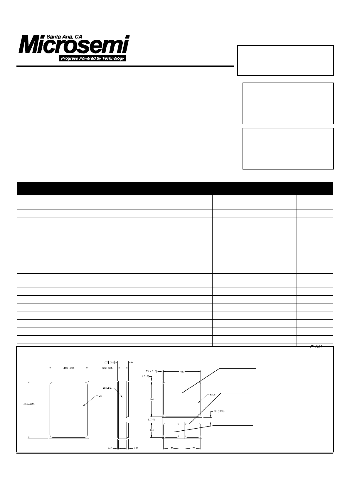
Mechanical Outline
Datasheet# MSC0295A
2830 S. Fairview St.
Santa Ana, CA 92704
PH: (714) 979-8220
FAX: (714) 966-5256
N-CHANNEL
INSULATED GATE
BIPOLAR TRANSISTOR
COLLECTOR
EMITTER (MS…A)
GATE (MS…B)

DESCRIPTION SYMBOL CONDITIONS MIN TYP. MAX UNIT
Collector-to-Emitter Breakdown Voltage
(Gate Shorted to Emitter)
BV
CES
VGS = 0 V, IC = 250 µA
1200 V
Gate Threshold Voltage V
GE(th)
VCE = VGE, IC = 350 µA
4.5 5.5 6.5 V
Gate-to-Emitter Leakage Current
I
GES
VGE = ± 20VDC, VCE = 0 TJ = 25°C
TJ = 125°C
±100
±200
nA
Collector-to-Emitter Leakage Current (Zero Gate
Voltage Collector Current) I
CES
VCE =0.8•BV
CES TJ
= 25°C
VGE
= 0 V TJ = 125°C
250
1000
µA
Collector-to-Emitter Saturation Voltage (1)
V
CE(sat)
VGE= 15V, IC= 25A TJ = 25°C
IC= 25A TJ = 125°C
IC= 60A TJ = 25°C
IC= 30A TJ = 125°C
2.7
3.3
3.4
4.3
3.2
3.9
V
Forward Transconductance (1) g
fs
VCE = 20 V; IC = 25 A 8.5 20 S
Input Capacitance
Output Capacitance
Reverse Transfer Capacitance
C
ies
C
oes
C
res
V
GE
= 0 V, VCE = 25 V, f = 1 MHz 1650
250
110
2200
380
160
pF
INDUCTIVE LOAD, Tj= 125°°C
Turn-on Delay Time
Rise Time
On Energy
Turn-off Delay Time
Fall Time
Off Energy
t
d(on)
t
ri
E
on
t
d(off)
t
fi
Eoff
VGE = 15 V, VCE = 600 V,
IC = 25 A, RG = 47 Ω,
L= 100 µH note 2, 3
75
65
3.6
420
45
2.4
110
100
560
60
ns
ns
mJ
ns
ns
mJ
INDUCTIVE LOAD, Tj= 125°°C
Turn-on Delay Time
Rise Time
On Energy
Turn-off Delay Time
Fall Time
Off Energy
t
d(on)
t
ri
E
on
t
d(off)
t
fi
Eoff
VGE = 15 V, VCE = 600 V,
IC = 50 A, RG = 47 Ω,
L= 100 µH note 2, 3
95
90
10
420
45
4.2
ns
ns
mJ
ns
ns
mJ
Total Gate Charge
Gate-to-Emitter Charge
Gate-to-Collector (Miller) Charge
Q
g
Q
ge
Q
gc
VGE = 15 V, VCE = 600V, IC = 25A 160
20
75
nC
Antiparallel diode forward voltage (MSAHZ52F120A
only)
V
F
IE= 10 A TJ = 25 °C
IE= 10 A TJ = 100 °C
2.4
2
3 V
V
Antiparallel diode reverse recovery time
(MSAHZ52F120A only)
t
rr
IE= 10 A, dIE/dt= 100 A/us, TJ= 25°C
IE= 10 A, dIE/dt= 800 A/us, TJ= 125°C
60
TBD ns
ns
Antiparallel diode reverse recovery charge
(MSAHZ52F120A only)
Q
rr
IE= 10 A, dIE/dt= 100 A/us, TJ= 25°C
IE= 10 A, dIE/dt= 800 A/us, TJ= 125°C
800
TBD nC
nC
Antiparallel diode peak recovery current
(MSAHZ52F120A only)
I
RM
IE= 10 A, dIE/dt= 100 A/us, TJ= 25°C
IE= 10 A, dIE/dt= 800 A/us, TJ= 125°C
22
TBD A
A
Electrical Parameters @ 25°°C (unless otherwise specified)
Notes
(1) Pulse test, t ≤≤ 300 µµs, duty cycle δδ ≤≤ 2%
(2) switching times and losses may increase for larger VCE and/or RG values or higher junction temperatures.
(3) switching losses include “tail” losses
(4) Microsemi Corp. does not manufacture the igbt die; contact company for details.
MSAGZ52F120A
MSAHZ52F120A
 Loading...