Microsemi Corporation MSAGA11F120D Datasheet

2830 S. Fairview Street
I
GES
Gate-Emitter Leakage Current (V
GE
= ±25V,
V
CE
=0V),
Tj= 37
°
C
Santa Ana, CA 92704
Phone: (714) 979-8220
Fax: (714) 559-5989
MSAGA11F120D
Fast IGBT Die for Implantable
Cardio Defibrillator
Applications
DESCRIPTION:
• N-Channel enhancement mode high density IGBT die
• Passivation: Polyimide, 20 um, over Silicon Nitride, .8um
• Emitter Metallization: Al/1%Si for aluminum wire bonding, 3.2 um typical.
• Collector/Gate Metallization: Ti – Ni (1 um) – Ag (0.2 um) for soft solder attach
55
FEATURES:
• Low Forward Voltage Drop, Low Tail Current
• Avalanche and Surge Rated
• High Freq. Switching to 20KHz
• Ultra Low Leakage Current
• RBSOA and SCSOA Rated
• Available with Lot Acceptance Testing Spec MSAGA11F120DL, "-L" Suffix
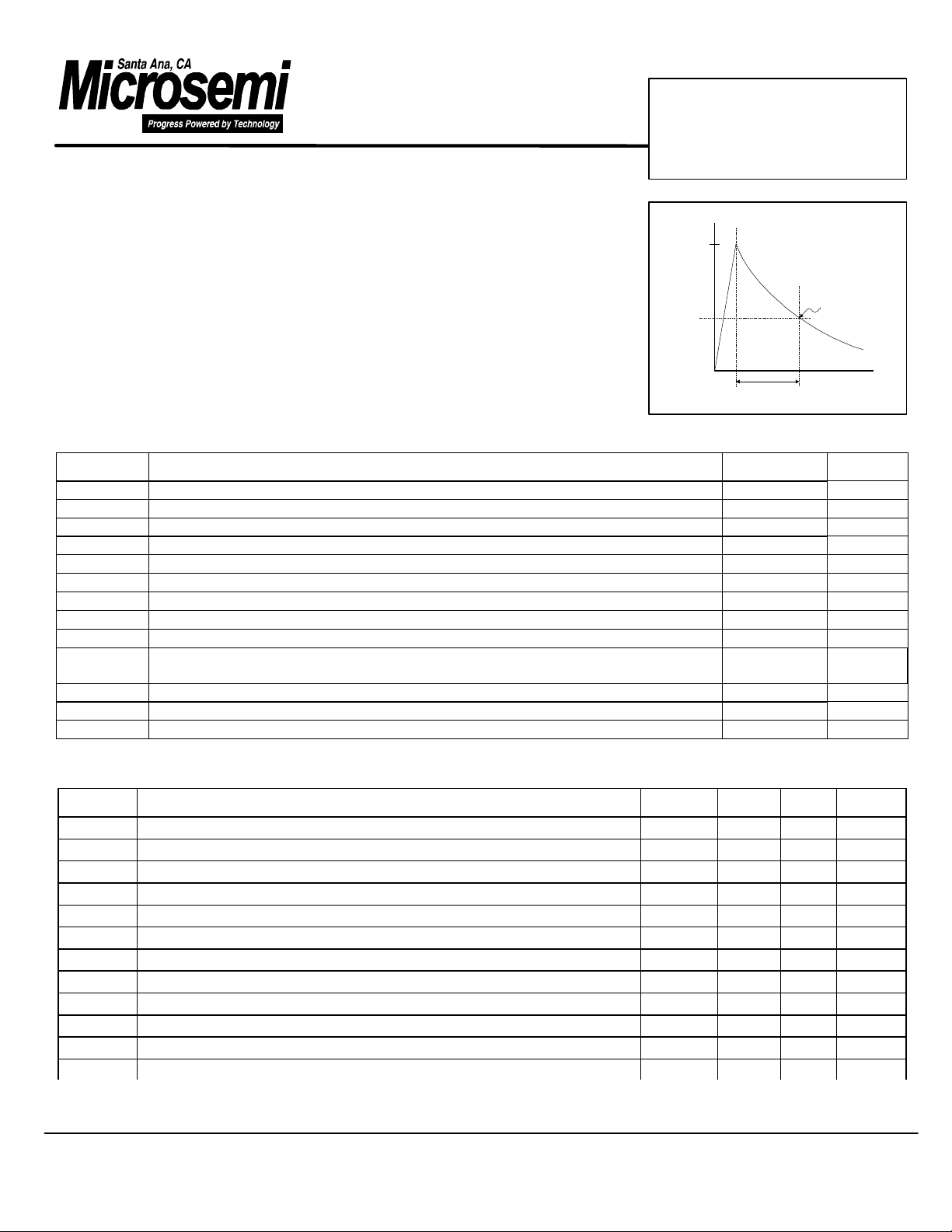
10µs x 4ms double exponential
Surge Current (ICM) - Amps
10µs 4000µs
35-50% of
ICM Max
MAXIMUM RATINGS:
SYMBOL PARAMETER VALUE UNIT
V
CES
V
CGR
V
EG
V
GE
I
C1
I
C2
I
CM
I
CM1
I
CM2
I
Csurge2
Collector-Emitter Voltage 1200 Volts
Collector-Gate Voltage (RGE = 20KΩ)
1200 Volts
Emitter-Collector Voltage 15 Volts
Gate-Emitter Voltage ±20 Volts
Continuous Collector Current @ TC = 25°C
Continuous Collector Current @ TC = 110°C
Surge Current (10µs x 4ms double exponential, see figure 2)
Pulsed Collector Current ¬ @ TC = 25°C
Pulsed Collector Current ¬ @ TC = 110°C
Surge Current: tp= 2 us (ton= 1.5 µs; toff= 0.5 µs to 50% decay), 10 pulses, duty
22 Amps
11 Amps
55 Amps
44 Amps
22 Amps
400 Apk
cycle= 1:2,500,000 (12 pulses/minute)
E
AS
P
D
T
J, TSTG
Single Pulse Avalanche Energy - 10 mJ
Total Power Dissipation 125 Watts
Operating and Storage: Junction Temperature Range -55 to 150
STATIC ELECTRICAL CHARACTERISTICS:
SYMBOL CHARACTERISTIC / TEST CONDITIONS MIN TYP MAX UNIT
BV
CES
RBV
CES
VGE(TH) Gate Threshold Voltage (V
Collector-Emitter Breakdown Voltage (VGE = 0V, IC = 0.5mA)
Collector-Emitter Reverse Breakdown Voltage® (V
Gate Threshold Voltage (V
= VGE, IC = 350µA, T
CE
= VGE, IC = 350µA, T
CE
VCE (ON) Collector-Emitter On Voltage (V
Collector-Emitter On Voltage (V
Collector-Emitter On Voltage (V
I
CES
Collector Cut-off Current (V
Collector Cut-off Current (V
Collector Cut-off Current (V
= 80%V
CE
= 80%V
CE
= 80%V
CE
Gate-Emitter Leakage Current (V
= 15V, IC = I
GE
= 15V, IC = I
GE
= 15V, IC = I
GE
, VGE = 0V, TJ = 25°C)
CES
, VGE = 0V, TJ = 37°C)
CES
, VGE = 0V, TJ = 125°C)
CES
= ±25V, VCE =0V)
GE
= 20V, IC = 10mA)
GE
= 37°C
J
= 25°C
J
= 25°C)
C2, TJ
= 37°C)
C2, TJ
= 125°C)
C2, TJ
1200 Volts
-15 Volts
5.7 Volts
4.5 5.5 6.5 Volts
3.1 3.5 Volts
3.5 Volts
4 4.5 Volts
0.02 10 uA
0.07 uA
1000 uA
2 ±100 nA
4 nA
°C
MSC0947.PDF 2/5/99 All Ratings: Device Packaged in TO-3 or Microsemi CoolPack Package, T
= 25°C unless otherwise specified
C

MSAGA11F120D
Fast IGBT Die for Implantable
Cardio Defibrillator
Applications
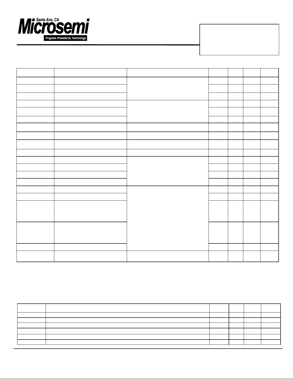
DYNAMIC CHARACTERISTICS:
SYMBOL CHARACTERISTIC TEST CONDITIONS MIN TYP MAX UNIT
C
ies
C
oes
C
ros
Input Capacitance
Output Capacitance
Reverse Transfer Capacitance f = 1 MHz 38 55 pF
Qg Total Gate Charge ¯
Qge Gate-Emitter Charge
Qgc Gate-Collector ("Miller") Charge
td (on)
t
r
td (off)
t
f
td (on)
t
r
td (off)
t
f
td (on)
t
r
td (off)
Turn-on Delay Time
Rise Time
Turn-off Delay Time
Fall Time
Turn-On Delay Time
Rise Time
Turn-off Delay Time
Fall Time
Turn-off Delay Time
Rise Time
Turn-off Delay Time
(tsv)
V
= 0V
GE
V
= 25V
CE
VGE = 15V
VCC = 0.5V
I
C
= I
CES
C2
Resistive Switching (25°C)
VGE = 15V, VCC = 0.5V
I
= I
C
C2
R
= 150Ω
e
CES
Inductive Switching (25°C)
V
R
(PEAK) = 0.5V
CLAMP
VGE = 15V, I
= 150Ω, TJ = +25°C
G
C
= I
C2
CES
Inductive Switching (125°C)
V
(PEAK) = 0.5V
CLAMP
VGE = 15V, I
C
= I
CES
C2
600 720 pF
60 120 pF
60 nC
4 nC
36 nC
35 ns
120 ns
580 ns
260 ns
55 110 ns
50 100 ns
380 570 ns
80 120 ns
40 ns
100 ns
550
ns
700
(tsi)
t
f
Fall Time
(tfv)
R
= 150Ω, TJ = +125°C
G
160
40
(tfi)
E
off
gfe Forward Transconductance
¬ Repetitive Rating: Pulse width limited by maximum junction temperature.
- IC = I
® TJ = 150°C
¯ See MIL-STD-750 Method 3471
= 50V, RCE = 25Ω, L = 300µH, TJ = 25°C
C2, VCC
Turn-off Switching Energy 1 mJ
V
=20V, IC = I
CE
C2
4.5 5 S
DIE PROBE PARAMETERS (100% TESTS):
SYMBOL CHARACTERISTIC / TEST CONDITIONS MIN TYP MAX UNIT
BV
CES
RBV
CES
VGE(TH)
VCE (ON)
I
CES
I
GES
MSC0947.PDF 2/5/99 All Ratings: Device Packaged in TO-3 or Microsemi CoolPack Package, T
Collector-Emitter Breakdown Voltage (VGE = 0V, IC = 0.5mA) 1200 1400 Volts
Collector-Emitter Reverse Breakdown Voltage ® (V
Gate Threshold Voltage (VCE = 6.5 V, IC = 350µA, TJ = 25°C
Collector-Emitter On Voltage (VGE = 12V, IC = 1 A, TJ = 25°C)
Collector Cut-off Current (VCE = 1200 V, VGE = 0V, TJ = 25°C)
Gate-Emitter Leakage Current (VGE = ±20 V, VCE =0V) 5 ±120 nA
= 15V, IC = 10mA) -15 30
GE
4.6 5.5 6.5
= 25°C unless otherwise specified
C
1.45 2.0
0.15 400 uA
ns
 Loading...