

Microsemi Corporation MSAER30N20A, MSAFR30N20A Datasheet
2830 S. Fairview St.
Santa Ana, CA 92704
PH: (714) 979-8220
FAX: (714) 966-5256
MSAER30N20A
MSAFR30N20A
Features
• Ultrafast rectifier in parallel with the body diode (MSAE type only)
• Rugged polysilicon gate cell structure
• Increased Unclamped Inductive Switching (UIS) capability
• Hermetically sealed, surface mount power package
• Low package inductance
• Very low thermal resistance
• Reverse polarity available upon request
ENHANCEMENT MODE
Maximum Ratings @ 25°°C (unless otherwise specified)
DESCRIPTION SYMBOL MAX. UNIT
200 Volts
30 Amps
85 mΩΩ
N-CHANNEL
POWER MOSFET
Drain-to-Source Breakdown Voltage (Gate Shorted to Source)
@ TJ ≥ 25°C
Drain-to-Gate Breakdown Voltage @ T
≥ 25°C, RGS= 1 MΩ BV
J
BV
Continuous Gate-to-Source Voltage V
Transient Gate-to-Source Voltage V
Continuous Drain Current Tj= 25°C
Tj=
100°C
Peak Drain Current, pulse width limited by T
Jmax
I
I
D100
I
Repetitive Avalanche Current I
Repetitive Avalanche Energy E
Single Pulse Avalanche Energy E
Voltage Rate of Change of the Recovery Diode
@ I
≤ IDM, di/dt ≤ 100 A/µs, VDD ≤ V
S
, TJ ≤ 150°C
DSS
dv/dt 5.0 V/ns
Power Dissipation P
Junction Temperature Range T
Storage Temperature Range T
Continuous Source Current (Body Diode) I
Pulse Source Current (Body Diode) I
Thermal Resistance, Junction to Case
θ
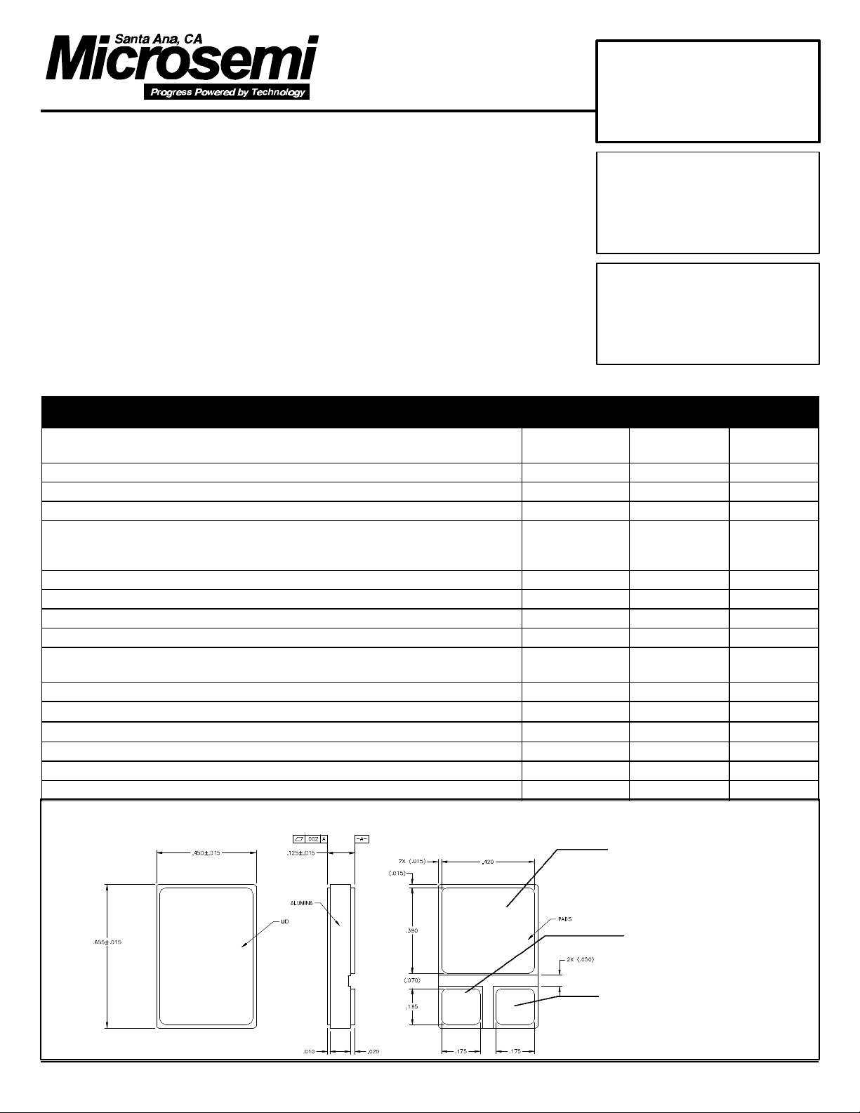
Mechanical Outline
DSS
DGR
GS
GSM
D25
DM
AR
AR
AS
D
stg
S
SM
JC
200 Volts
200 Volts
+/-20 Volts
+/-30 Volts
30
Amps
19
120 Amps
30 Amps
15 mJ
200 mJ
300 Watts
j
-55 to +150
-55 to +150
°C
°C
30 Amps
120 Amps
0.4
DRAIN
°C/W
Datasheet# MSC0256B
SOURCE
GATE

MSAER30N20A
MSAFR30N20A
Electrical Parameters @ 25°°C (unless otherwise specified)
DESCRIPTION SYMBOL CONDITIONS MIN TYP. MAX UNIT
Drain-to-Source Breakdown Voltage
(Gate Shorted to Source)
Temperature Coefficient of the Drain-to-Source
Breakdown Voltage
Gate Threshold Voltage V
Gate-to-Source Leakage Current
Drain-to-Source Leakage Current (Zero Gate
Voltage Drain Current) I
Static Drain-to-Source On-State Resistance (1)
Forward Transconductance (1) g
∆BV
BV
R
DSS
GS(th)
I
GSS
DSS
DS(on)
DSS
fs
/∆T
VGS = 0 V, ID = 250 µA
J
200 V
0.29
VDS = VGS, ID = 1 mA 2.0 4.0 V
VGS = ± 20VDC, VDS = 0 TJ = 25°C
TJ = 125°C
VDS =0.8•BV
VGS
DSS TJ
= 0 V TJ = 125°C
= 25°C
VGS= 10V, ID= 20A TJ = 25°C
ID= 30A TJ = 25°C
ID= 20A TJ = 125°C
VDS ≥ 15 V; ID = 20 A
9 S
1.5
±100
±200
25
250
0.085
0.090
V/°C
nA
µA
Ω
Input Capacitance
Output Capacitance
Reverse Transfer Capacitance
Turn-on Delay Time
T
Rise Time
Turn-off Delay Time
Fall Time
Total Gate Charge
Q
Gate-to-Source Charge
Gate-to-Drain (Miller) Charge
Body Diode Forward Voltage (1) V
Reverse Recovery Time (Body Diode) t
Reverse Recovery Charge Q
C
C
C
t
d(off)
Q
Q
oss
rss
d(on)
t
t
g(on)
SD
rr
V
iss
= 0 V, VDS = 25 V, f = 1 MHz 3500
GS
pF
700
110
VGS = 10 V, VDS = 100 V,
r
ID = 30 A, RG = 2.35 Ω
35
190
ns
170
f
VGS = 10 V, VDS = 100V, ID = 30A 55
gs
gd
8
30
IF = IS, VGS = 0 V MSAE
MSAF
IF = 10 A, MSAE
-di/dt = 100 A/µs, MSAF
rr
IF = 10 A, MSAE
di/dt = 100 A/µs, MSAF
130
115
22
60
1.2
1.9
50
950
tbd
9
nC
V
ns
µC
Notes
(1) Pulse test, t ≤≤ 300 µµs, duty cycle δδ ≤≤ 2%
(2) Microsemi Corp. does not manufacture the mosfet die; contact company for details.
 Loading...