Symbol
Parameter
Value
Unit
P
DISS
Power Dissipation * (TC ≤≤ 85°°C)
75
W
I
C
Device Current *
3.5
A
V
CC
Collector - Supply Voltage *
40
V
T
J
Junction Temperature (Pulsed RF Operation)
250
°°
C
T
STG
Storage Temperature
- 65 to + 200
°°
C
R
TH(j-c)
Junction-Case Thermal Resistance
2.2
°°
C/W
140 COMMERCE DRIVE
FAX: (215) 631-9855
MONTGOMERYVILLE, PA
18936-1013
PHONE: (215) 631-9840
RF & MICROWAVE TRANSISTORS
SPECIALITY AVIONICS/JTIDS APPLICATIONS
Features
• • REFRACTORY/GOLD METALLIZATION
• • EMITTER SITE BALLASTED
• • 15:1 VSWR CAPABILITY
• • LOW RF THERMAL RESISTANCE
• • INPUT/OUTPUT MATCHING
• • OVERLAY GEOMETRY
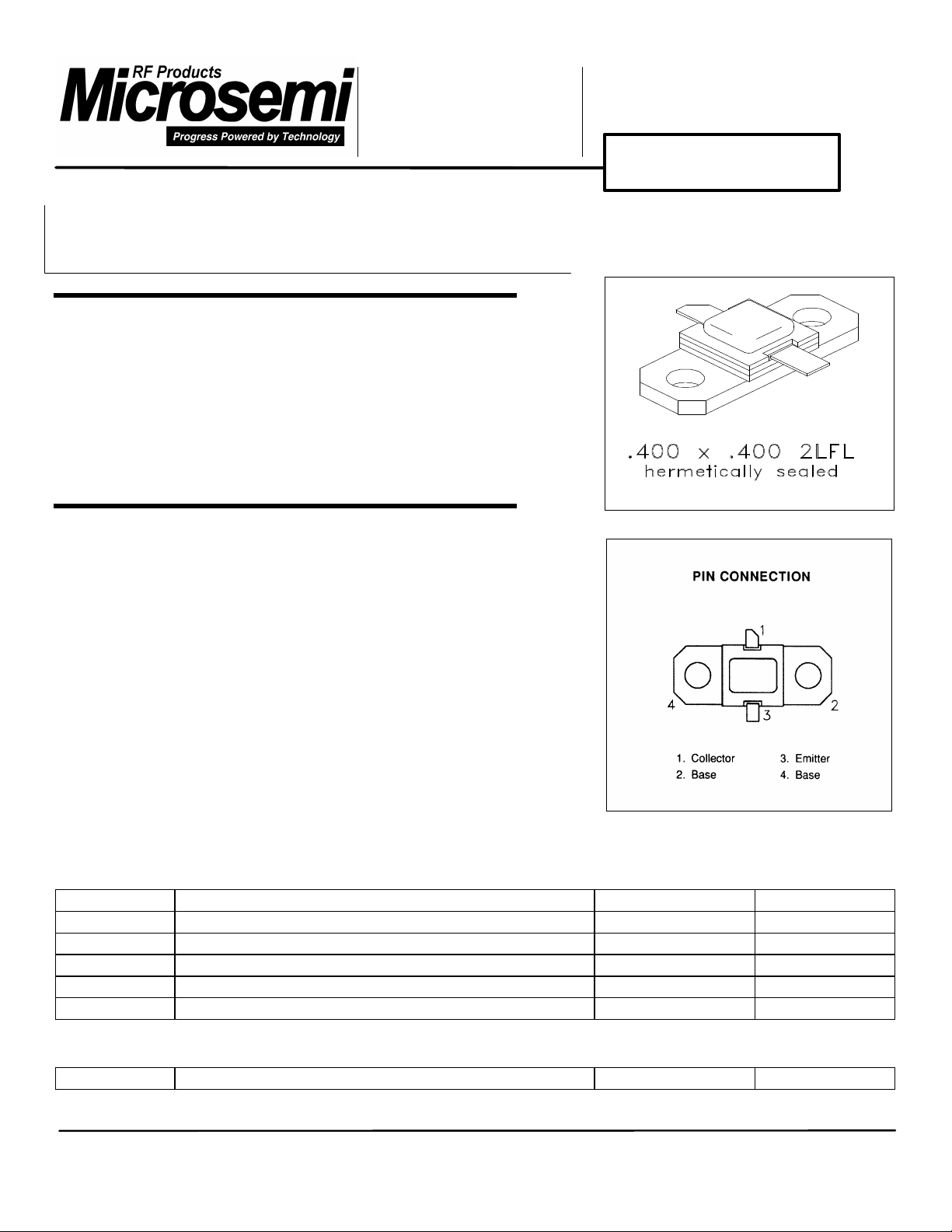
• • METAL/CERAMIC HERMETIC PACKAGE
• • P
= 30 W MIN. WITH 7.8 dB Gain
OUT
MS2213
DESCRIPTION:DESCRIPTION:
The MS2213 device is a high power Class C transistor specifically
designed for JTIDS pulsed output and driver applications.
The device is capable of operation over a wide range of pulse
widths, duty cycles and temperatures and is capable of
withstanding 15:1 output VSWR at rated RF conditions.
Low RF thermal resistance and computerized automatic wire
bonding techniques ensure high reliability and product
consistency.
The MS2213 is supplied in the hermetic metal/ceramic package
with internal input matching structures.
AABSOLUTE MAXIMUM RATINGSBSOLUTE MAXIMUM RATINGS (Tcase = 25°°C)
Thermal DataThermal Data
* Applies only to rated RF amplifier operation
MSC0920.PDF 9-23-98

ELECTRICAL SPECIFICATIONS (ELECTRICAL SPECIFICATIONS (Tcase = 25Tcase = 25°°C)C)
Symbol
Test Conditions
Value
Min.
Typ.
Max.
Unit
BV
CBO
I
C
55
----
----VBV
EBO
I
E
3.5
----
----
V
I
C
R
BE
55
----
----VI
CES
V
CE
----
----
5.0mAh
FE
V
CE
I
C
15
----
150
----
Symbol
Test Conditions
Value
Min.
Typ.
Max.
Unit
V
CC
3036----
W
V
CC
4045----
%
STATICSTATIC
= 10 mA
= 1 mA
BV
CER
= 20 mA
= 35 V
= 5V
=10Ω
= 1.0 A
MS2213
DYNAMICDYNAMIC
P
OUT
VV
C
G
P
Note: Pulse format: 6.4 µµs on 6.6 µµs off, repeat for 3.3 ms, then off for 4.5125 ms.
Duty Cycle: Burst 49.2%, Overall 20.8%
f = 960 - 1215 MHz PIN = 5.0 W
f = 960 - 1215 MHz PIN = 5.0 W
f = 960 - 1215 MHz PIN = 5.0 W VCC = +35 V 7.8 8.6 ---- dB
= +35 V
= +35 V
MSC0920.PDF 9-23-98
