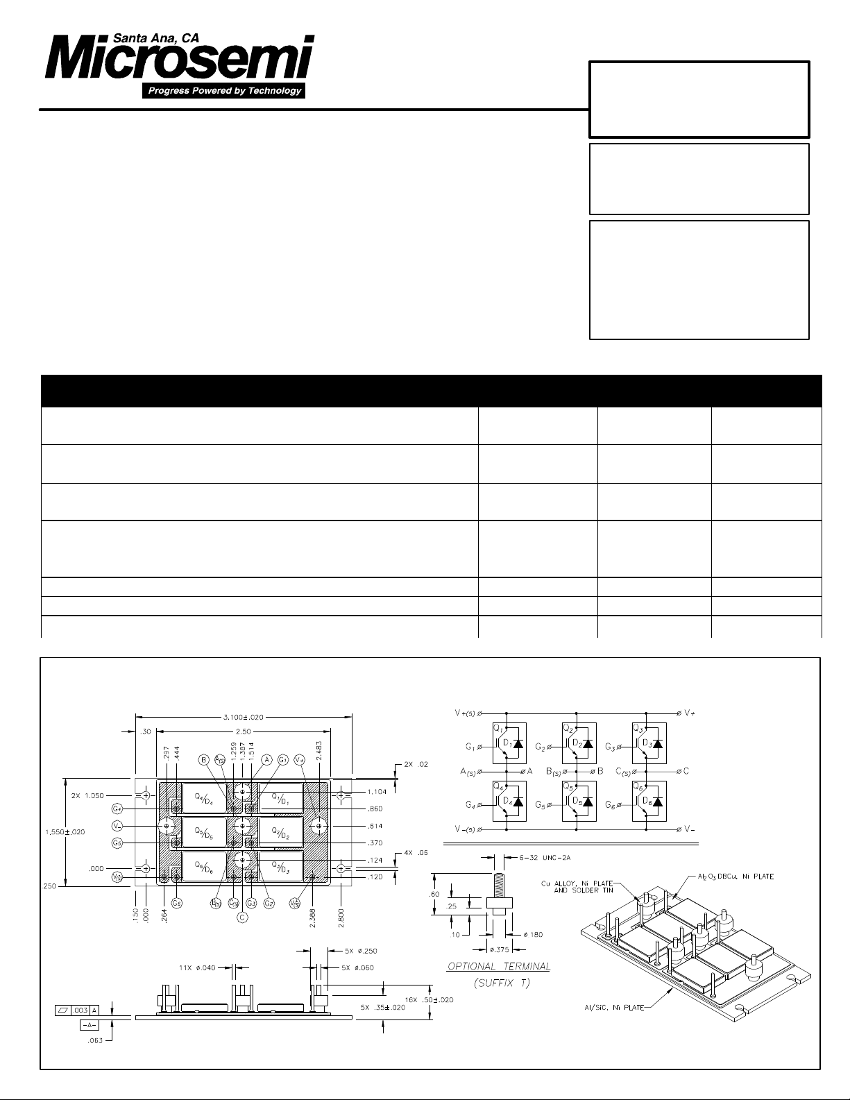
Microsemi Corporation MM118-06, MM118-12 Datasheet

150 Amps
2830 S. Fairview St.
Santa Ana, CA 92704
PH: (714) 979-8220
FAX: (714) 966-5256
MM118-XX
Features
• Available in Low Conduction Loss Class as MM118-xxL or Fast
Switching Class as MM118-xxF
• Compact and rugged construction offering weight and space savings
• Available with PC board solderable pins (see mechanical outline below)
or threaded terminals (add “T” suffix to part number, see option below)
• HPM (Hermetic Power Module)
• Isolation voltage capability (in reference to the base) in excess of 3kV
• Very low thermal resistance
• Thermally matched construction provides excellent temperature and
power cycling capability
600 / 1200 Volts
3 PHASE N-CHANNEL
INSULATED GATE
TRANSISTOR (IGBT)
Maximum Ratings per switch @ 25°C (unless otherwise specified)
PART NUMBER SYMBOL MM118-06 MM118-12
SERIES
BIPOLAR
BRIDGE
Collector-to-Emitter Breakdown Voltage (Gate shorted to
Emitter), @ Tj≥ 25°C
Collector-to-Gate Breakdown Voltage @ Tj≥ 25°C, RGS= 1
MΩ
Gate-to-Emitter Voltage continuous
transient
Continuous Collector Current Tj=
25°C
Tj= 90°C
Peak Collector Current, pulsewidth limited by T
Power Dissipation P
Thermal resistance, junction to base per switch
j max
BV
BV
V
V
I
I
RΘjc, max
GES
GEM
C25
C90
I
CM
CES
CGR
D
600 V 1200 V
600 V 1200 V
+/- 20 V
+/- 30 V
60 A
32 A
120 A 104 A
165 W 165 W
0.75°C/W
+/- 20 V
+/- 30 V
52 A
33 A
0.75°C/W
Mechanical Outline
Datasheet# MSC0321A

MM-XX SERIES
Maximum Ratings @ 25°C (unless otherwise specified) - continued
DESCRIPTION SYMBOL MM118-06 MM118-12
Short Circuit Reverse Current (RBSOA) @ Tj= 125°C, V
Junction and Storage Temperature Range (°C)
Continuous Source Current (parallel Diode) I
Pulse Source Current (parallel Diode) I
= 0.8 x V
CE
CES
I
T
j, Tstg
max
S
SM
64 A 66 A
-55 to +150 -55 to +150
60 A 50 A
100 A 100 A
Electrical Parameters, per switch @ 25°C (unless otherwise specified)
DESCRIPTION
Collector-to-Emitter Breakdown Voltage
(Gate Shorted to Emitter)
Gate Threshold Voltage V
Gate-to-Emitter Leakage Current
Collector-to-Emitter Leakage Current
(Zero Gate Voltage Collector Current) I
Collector-to-Emitter Saturation Voltage
(1) V
Forward Transconductance (1) g
Input Capacitance
Output Capacitance
Reverse Transfer Capacitance
INDUCTIVE LOAD, Tj= 25°C (2,3)
Turn-on Delay Time
Rise Time
On Energy
Turn-off Delay Time
Fall Time
Off Energy
SYMBOL
BV
CES
GE(th)
I
GES
CES
CE(sat)
fs
C
ies
C
oes
C
res
t
d(on)
t
ri
E
on
t
d(off)
t
fi
Eoff
CONDITIONS
VGS = 0 V, IC = 250 µA
VCE = VGE, IC = 250 µA
VCE = VGE, IC = 2.5 mA
VCE = VGE, IC = 350 µA
VGE = ± 20VDC, VCE = 0 TJ = 25°C
TJ = 125°C
VCE =0.8•BV
VGE
VGE= 15V, IC= 30A TJ = 25°C
IC= 60A TJ = 25°C
IC= 30A TJ = 125°C
IC= 30A TJ = 25°C
VGE= 15V, IC= 25A TJ = 25°C
IC= 50A TJ = 25°C
IC= 25A TJ = 125°C
VCE ≥ 10 V; IC = 30 A
VCE ≥ 10 V; IC = 30 A
CES TJ
= 0 V TJ = 125°C
V
= 0 V, VCE = 25 V, f = 1 MHz MM118-06F
GE
VGE = 15 V, L= 100 µH note 2, 3
for MM118-06: VCE = 480 V,
IC = 30 A, RG = 4.7 Ω
for MM118-12: VCE= 600 V,
IC= 25 A, RG = 47 Ω
= 25°C
PART MIN TYP. MAX UNIT
MM118-06
MM118-12
MM118-06F
MM118-06L
MM118-12
(ALL)
(ALL) 200
MM118-06F
MM118-06F
MM118-06F
MM018-06L
MM118-12
MM118-12
MM118-12
MM118-06F
MM118-06L
MM118-12
MM118-06L
MM118-12
MM118-06F
MM118-06L
MM118-12
MM118-06F
MM118-06L
MM118-12
MM118-06F
MM118-06L
MM118-12
MM118-06F
MM118-06L
MM118-12
MM118-12
MM118-06F
MM118-06L
MM118-12
MM118-06F
MM118-06L
MM118-12
MM118-06F
MM118-06L
MM118-12
600
1200
2.5
4
4.5
15
7
8.5
4
5.5
2.2
3.5
2.2
2.2
2.7
3.4
3.3
20
13
20
2500
2760
1650
230
240
250
70
51
110
25
60
75
30
130
65
3.6
175
400
420
125
400
45
1.3
5
2.4
5.0
7
6.5
±100
±200
1000
2.9
tbd
tbd
2.5
3.2
tbd
3.9
tbd
tbd
2200
tbd
tbd
380
tbd
tbd
160
tbd
tbd
110
tbd
tbd
100
tbd
tbd
560
175
tbd
60
-
-
-
V
V
nA
µA
V
S
pF
ns
ns
ns
ns
ns
ns
mJ
ns
ns
ns
ns
ns
ns
mJ
mJ
mJ
Datasheet# MSC0321A
 Loading...