

Page 1

UG0445
User Guide
SmartFusion2 SoC FPGA and IGLOO2 FPGA Fabric
Page 2

Microsemi Headquarters
One Enterprise, Aliso Viejo,
CA 92656 USA
Within the USA: +1 (800) 713-4113
Outside the USA: +1 (949) 380-6100
Sales: +1 (949) 380-6136
Fax: +1 (949) 215-4996
Email: sales.support@microsemi.com
www.microsemi.com
©2019 Microsemi, a wholly owned
subsidiary of Microchip Technology Inc. All
rights reserved. Microsemi and the
Microsemi logo are registered trademarks of
Microsemi Corporation. All other trademarks
and service marks are the property of their
respective owners.
Microsemi makes no warranty, representation, or guarantee regarding the information contained herein or the suitability of
its products and services for any particular purpose, nor does Microsemi assume any liability whatsoever arising out of the
application or use of any product or circuit. The products sold hereunder and any other products sold by Microsemi have
been subject to limited testing and should not be used in conjunction with mission-critical equipment or applications. Any
performance specifications are believed to be reliable but are not verified, and Buyer must conduct and complete all
performance and other testing of the products, alone and together with, or installed in, any end-products. Buyer shall not
rely on any data and performance specifications or parameters provided by Microsemi. It is the Buyer’s responsibility to
independently determine suitability of any products and to test and verify the same. The information provided by Microsemi
hereunder is provided “as is, where is” and with all faults, and the entire risk associated with such information is entirely
with the Buyer. Microsemi does not grant, explicitly or implicitly, to any party any patent rights, licenses, or any other IP
rights, whether with regard to such information itself or anything described by such information. Information provided in this
document is proprietary to Microsemi, and Microsemi reserves the right to make any changes to the information in this
document or to any products and services at any time without notice.
About Microsemi
Microsemi, a wholly owned subsidiary of Microchip Technology Inc. (Nasdaq: MCHP), offers a comprehensive portfolio of
semiconductor and system solutions for aerospace & defense, communications, data center and industrial markets.
Products include high-performance and radiation-hardened analog mixed-signal integrated circuits, FPGAs, SoCs and
ASICs; power management products; timing and synchronization devices and precise time solutions, setting the world's
standard for time; voice processing devices; RF solutions; discrete components; enterprise storage and communication
solutions, security technologies and scalable anti-tamper products; Ethernet solutions; Power-over-Ethernet ICs and
midspans; as well as custom design capabilities and services. Learn more at www.microsemi.com.
50200445 . 7.0 4/19
Page 3

Contents
1 Revision History . . . . . . . . . . . . . . . . . . . . . . . . . . . . . . . . . . . . . . . . . . . . . . . . . . . . . 1
1.1 Revision 7.0 . . . . . . . . . . . . . . . . . . . . . . . . . . . . . . . . . . . . . . . . . . . . . . . . . . . . . . . . . . . . . . . . . . . . . . . 1
1.2 Revision 6.0 . . . . . . . . . . . . . . . . . . . . . . . . . . . . . . . . . . . . . . . . . . . . . . . . . . . . . . . . . . . . . . . . . . . . . . . 1
1.3 Revision 5.0 . . . . . . . . . . . . . . . . . . . . . . . . . . . . . . . . . . . . . . . . . . . . . . . . . . . . . . . . . . . . . . . . . . . . . . . 1
1.4 Revision 4.0 . . . . . . . . . . . . . . . . . . . . . . . . . . . . . . . . . . . . . . . . . . . . . . . . . . . . . . . . . . . . . . . . . . . . . . . 1
1.5 Revision 3.0 . . . . . . . . . . . . . . . . . . . . . . . . . . . . . . . . . . . . . . . . . . . . . . . . . . . . . . . . . . . . . . . . . . . . . . . 1
1.6 Revision 2.0 . . . . . . . . . . . . . . . . . . . . . . . . . . . . . . . . . . . . . . . . . . . . . . . . . . . . . . . . . . . . . . . . . . . . . . . 2
1.7 Revision 1.0 . . . . . . . . . . . . . . . . . . . . . . . . . . . . . . . . . . . . . . . . . . . . . . . . . . . . . . . . . . . . . . . . . . . . . . . 2
1.8 Revision 0.0 . . . . . . . . . . . . . . . . . . . . . . . . . . . . . . . . . . . . . . . . . . . . . . . . . . . . . . . . . . . . . . . . . . . . . . . 2
2 Fabric Architecture . . . . . . . . . . . . . . . . . . . . . . . . . . . . . . . . . . . . . . . . . . . . . . . . . . 3
2.1 Introduction . . . . . . . . . . . . . . . . . . . . . . . . . . . . . . . . . . . . . . . . . . . . . . . . . . . . . . . . . . . . . . . . . . . . . . . 3
2.2 Fabric Resources . . . . . . . . . . . . . . . . . . . . . . . . . . . . . . . . . . . . . . . . . . . . . . . . . . . . . . . . . . . . . . . . . . . 4
2.3 Architecture Overview . . . . . . . . . . . . . . . . . . . . . . . . . . . . . . . . . . . . . . . . . . . . . . . . . . . . . . . . . . . . . . . 5
2.3.1 Logic Element . . . . . . . . . . . . . . . . . . . . . . . . . . . . . . . . . . . . . . . . . . . . . . . . . . . . . . . . . . . . . . 5
2.3.2 Interface Logic Element . . . . . . . . . . . . . . . . . . . . . . . . . . . . . . . . . . . . . . . . . . . . . . . . . . . . . . . 6
2.3.3 I/O Module . . . . . . . . . . . . . . . . . . . . . . . . . . . . . . . . . . . . . . . . . . . . . . . . . . . . . . . . . . . . . . . . . 6
2.3.4 FPGA Routing Architecture . . . . . . . . . . . . . . . . . . . . . . . . . . . . . . . . . . . . . . . . . . . . . . . . . . . . 7
2.4 Fabric Array Coordinate System . . . . . . . . . . . . . . . . . . . . . . . . . . . . . . . . . . . . . . . . . . . . . . . . . . . . . . 10
3 LSRAM . . . . . . . . . . . . . . . . . . . . . . . . . . . . . . . . . . . . . . . . . . . . . . . . . . . . . . . . . . 13
3.1 Introduction . . . . . . . . . . . . . . . . . . . . . . . . . . . . . . . . . . . . . . . . . . . . . . . . . . . . . . . . . . . . . . . . . . . . . . 13
3.1.1 Features . . . . . . . . . . . . . . . . . . . . . . . . . . . . . . . . . . . . . . . . . . . . . . . . . . . . . . . . . . . . . . . . . 13
3.2 LSRAM Resources . . . . . . . . . . . . . . . . . . . . . . . . . . . . . . . . . . . . . . . . . . . . . . . . . . . . . . . . . . . . . . . . 13
3.3 Functional Description . . . . . . . . . . . . . . . . . . . . . . . . . . . . . . . . . . . . . . . . . . . . . . . . . . . . . . . . . . . . . . 14
3.3.1 Port List . . . . . . . . . . . . . . . . . . . . . . . . . . . . . . . . . . . . . . . . . . . . . . . . . . . . . . . . . . . . . . . . . . 15
3.3.2 Port Descriptions . . . . . . . . . . . . . . . . . . . . . . . . . . . . . . . . . . . . . . . . . . . . . . . . . . . . . . . . . . . 16
3.4 Memory Modes . . . . . . . . . . . . . . . . . . . . . . . . . . . . . . . . . . . . . . . . . . . . . . . . . . . . . . . . . . . . . . . . . . . 20
3.4.1 Dual-Port Mode . . . . . . . . . . . . . . . . . . . . . . . . . . . . . . . . . . . . . . . . . . . . . . . . . . . . . . . . . . . . 20
3.4.2 Two-Port Mode . . . . . . . . . . . . . . . . . . . . . . . . . . . . . . . . . . . . . . . . . . . . . . . . . . . . . . . . . . . . 21
3.5 Operating Modes . . . . . . . . . . . . . . . . . . . . . . . . . . . . . . . . . . . . . . . . . . . . . . . . . . . . . . . . . . . . . . . . . . 23
3.5.1 Read Operation . . . . . . . . . . . . . . . . . . . . . . . . . . . . . . . . . . . . . . . . . . . . . . . . . . . . . . . . . . . . 23
3.5.2 Write Operation . . . . . . . . . . . . . . . . . . . . . . . . . . . . . . . . . . . . . . . . . . . . . . . . . . . . . . . . . . . . 25
3.5.3 Reset Operation . . . . . . . . . . . . . . . . . . . . . . . . . . . . . . . . . . . . . . . . . . . . . . . . . . . . . . . . . . . 27
3.5.4 Block Select Operation . . . . . . . . . . . . . . . . . . . . . . . . . . . . . . . . . . . . . . . . . . . . . . . . . . . . . . 27
3.5.5 Collision . . . . . . . . . . . . . . . . . . . . . . . . . . . . . . . . . . . . . . . . . . . . . . . . . . . . . . . . . . . . . . . . . . 29
3.6 How to Use LSRAM . . . . . . . . . . . . . . . . . . . . . . . . . . . . . . . . . . . . . . . . . . . . . . . . . . . . . . . . . . . . . . . . 29
3.6.1 Design Flow . . . . . . . . . . . . . . . . . . . . . . . . . . . . . . . . . . . . . . . . . . . . . . . . . . . . . . . . . . . . . . . 29
3.6.2 LSRAM Use Model . . . . . . . . . . . . . . . . . . . . . . . . . . . . . . . . . . . . . . . . . . . . . . . . . . . . . . . . . 34
4 Micro SRAM (µSRAM) . . . . . . . . . . . . . . . . . . . . . . . . . . . . . . . . . . . . . . . . . . . . . . 37
4.1 Introduction . . . . . . . . . . . . . . . . . . . . . . . . . . . . . . . . . . . . . . . . . . . . . . . . . . . . . . . . . . . . . . . . . . . . . . 37
4.1.1 Features . . . . . . . . . . . . . . . . . . . . . . . . . . . . . . . . . . . . . . . . . . . . . . . . . . . . . . . . . . . . . . . . . 37
4.2 µSRAM Resource Table . . . . . . . . . . . . . . . . . . . . . . . . . . . . . . . . . . . . . . . . . . . . . . . . . . . . . . . . . . . . 37
4.3 Functional Description . . . . . . . . . . . . . . . . . . . . . . . . . . . . . . . . . . . . . . . . . . . . . . . . . . . . . . . . . . . . . . 38
4.3.1 Architecture Overview . . . . . . . . . . . . . . . . . . . . . . . . . . . . . . . . . . . . . . . . . . . . . . . . . . . . . . . 38
4.3.2 Port List . . . . . . . . . . . . . . . . . . . . . . . . . . . . . . . . . . . . . . . . . . . . . . . . . . . . . . . . . . . . . . . . . . 39
4.3.3 Port Description . . . . . . . . . . . . . . . . . . . . . . . . . . . . . . . . . . . . . . . . . . . . . . . . . . . . . . . . . . . . 40
4.4 Operating Modes . . . . . . . . . . . . . . . . . . . . . . . . . . . . . . . . . . . . . . . . . . . . . . . . . . . . . . . . . . . . . . . . . . 44
Microsemi Proprietary and Confidential UG0445 User Guide Revision 7.0 iii
Page 4

4.4.1 Read Operation . . . . . . . . . . . . . . . . . . . . . . . . . . . . . . . . . . . . . . . . . . . . . . . . . . . . . . . . . . . . 44
4.4.2 Write Operation . . . . . . . . . . . . . . . . . . . . . . . . . . . . . . . . . . . . . . . . . . . . . . . . . . . . . . . . . . . . 49
4.5 Reset Operation . . . . . . . . . . . . . . . . . . . . . . . . . . . . . . . . . . . . . . . . . . . . . . . . . . . . . . . . . . . . . . . . . . . 50
4.5.1 Collision . . . . . . . . . . . . . . . . . . . . . . . . . . . . . . . . . . . . . . . . . . . . . . . . . . . . . . . . . . . . . . . . . . 52
4.6 How to Use µSRAM . . . . . . . . . . . . . . . . . . . . . . . . . . . . . . . . . . . . . . . . . . . . . . . . . . . . . . . . . . . . . . . . 53
4.6.1 Design Flow . . . . . . . . . . . . . . . . . . . . . . . . . . . . . . . . . . . . . . . . . . . . . . . . . . . . . . . . . . . . . . . 53
5 Math Blocks . . . . . . . . . . . . . . . . . . . . . . . . . . . . . . . . . . . . . . . . . . . . . . . . . . . . . . . 56
5.1 Introduction . . . . . . . . . . . . . . . . . . . . . . . . . . . . . . . . . . . . . . . . . . . . . . . . . . . . . . . . . . . . . . . . . . . . . . 56
5.1.1 Features . . . . . . . . . . . . . . . . . . . . . . . . . . . . . . . . . . . . . . . . . . . . . . . . . . . . . . . . . . . . . . . . . 56
5.2 Math Block Resource Table . . . . . . . . . . . . . . . . . . . . . . . . . . . . . . . . . . . . . . . . . . . . . . . . . . . . . . . . . . 56
5.3 Functional Description . . . . . . . . . . . . . . . . . . . . . . . . . . . . . . . . . . . . . . . . . . . . . . . . . . . . . . . . . . . . . . 57
5.3.1 Architecture Overview . . . . . . . . . . . . . . . . . . . . . . . . . . . . . . . . . . . . . . . . . . . . . . . . . . . . . . . 57
5.4 How to Use Math Blocks . . . . . . . . . . . . . . . . . . . . . . . . . . . . . . . . . . . . . . . . . . . . . . . . . . . . . . . . . . . . 60
5.4.1 Design Flow . . . . . . . . . . . . . . . . . . . . . . . . . . . . . . . . . . . . . . . . . . . . . . . . . . . . . . . . . . . . . . . 60
5.4.2 Math Block Use Models . . . . . . . . . . . . . . . . . . . . . . . . . . . . . . . . . . . . . . . . . . . . . . . . . . . . . . 67
5.4.3 Coding Style Examples . . . . . . . . . . . . . . . . . . . . . . . . . . . . . . . . . . . . . . . . . . . . . . . . . . . . . . 72
6 I/Os . . . . . . . . . . . . . . . . . . . . . . . . . . . . . . . . . . . . . . . . . . . . . . . . . . . . . . . . . . . . . 77
6.1 Introduction . . . . . . . . . . . . . . . . . . . . . . . . . . . . . . . . . . . . . . . . . . . . . . . . . . . . . . . . . . . . . . . . . . . . . . 77
6.2 Functional Description . . . . . . . . . . . . . . . . . . . . . . . . . . . . . . . . . . . . . . . . . . . . . . . . . . . . . . . . . . . . . . 77
6.2.1 Transmit Buffer . . . . . . . . . . . . . . . . . . . . . . . . . . . . . . . . . . . . . . . . . . . . . . . . . . . . . . . . . . . . 79
6.2.2 Receive Buffer . . . . . . . . . . . . . . . . . . . . . . . . . . . . . . . . . . . . . . . . . . . . . . . . . . . . . . . . . . . . . 79
6.2.3 Low-Power Exit . . . . . . . . . . . . . . . . . . . . . . . . . . . . . . . . . . . . . . . . . . . . . . . . . . . . . . . . . . . . 80
6.2.4 On-Die Termination . . . . . . . . . . . . . . . . . . . . . . . . . . . . . . . . . . . . . . . . . . . . . . . . . . . . . . . . . 81
6.3 I/O Banks . . . . . . . . . . . . . . . . . . . . . . . . . . . . . . . . . . . . . . . . . . . . . . . . . . . . . . . . . . . . . . . . . . . . . . . . 81
6.4 Simultaneous Switching Noise . . . . . . . . . . . . . . . . . . . . . . . . . . . . . . . . . . . . . . . . . . . . . . . . . . . . . . . . 81
6.4.1 GND Bounce and V
6.5 Supported I/O Standards . . . . . . . . . . . . . . . . . . . . . . . . . . . . . . . . . . . . . . . . . . . . . . . . . . . . . . . . . . . . 87
6.5.1 Single-Ended Standards . . . . . . . . . . . . . . . . . . . . . . . . . . . . . . . . . . . . . . . . . . . . . . . . . . . . . 88
6.5.2 Voltage-Referenced Standards . . . . . . . . . . . . . . . . . . . . . . . . . . . . . . . . . . . . . . . . . . . . . . . . 88
6.5.3 Differential Standards . . . . . . . . . . . . . . . . . . . . . . . . . . . . . . . . . . . . . . . . . . . . . . . . . . . . . . . 89
6.6 I/O Programmable Features . . . . . . . . . . . . . . . . . . . . . . . . . . . . . . . . . . . . . . . . . . . . . . . . . . . . . . . . . 90
6.6.1 Programmable Slew-Rate Control . . . . . . . . . . . . . . . . . . . . . . . . . . . . . . . . . . . . . . . . . . . . . . 91
6.6.2 Programmable Input Delay . . . . . . . . . . . . . . . . . . . . . . . . . . . . . . . . . . . . . . . . . . . . . . . . . . . 92
6.6.3 Programmable Weak Pull-Up and Pull-Down . . . . . . . . . . . . . . . . . . . . . . . . . . . . . . . . . . . . . 92
6.6.4 Programmable Schmitt Trigger Receiver . . . . . . . . . . . . . . . . . . . . . . . . . . . . . . . . . . . . . . . . 93
6.6.5 Programmable Pre-emphasis . . . . . . . . . . . . . . . . . . . . . . . . . . . . . . . . . . . . . . . . . . . . . . . . . 93
6.6.6 Bus Keeper . . . . . . . . . . . . . . . . . . . . . . . . . . . . . . . . . . . . . . . . . . . . . . . . . . . . . . . . . . . . . . . 94
6.7 Receiver ODT Configuration . . . . . . . . . . . . . . . . . . . . . . . . . . . . . . . . . . . . . . . . . . . . . . . . . . . . . . . . . 95
6.7.1 Receiver ODT Configuration for MSIO and MSIOD Banks . . . . . . . . . . . . . . . . . . . . . . . . . . . 96
6.7.2 Receiver ODT Configuration for DDRIO Banks . . . . . . . . . . . . . . . . . . . . . . . . . . . . . . . . . . . . 97
6.8 Driver Impedance Configuration . . . . . . . . . . . . . . . . . . . . . . . . . . . . . . . . . . . . . . . . . . . . . . . . . . . . . 100
6.8.1 Driver Impedance Configuration for MSIO/MSIODs . . . . . . . . . . . . . . . . . . . . . . . . . . . . . . . 101
6.8.2 Driver Impedance Configuration for DDRIOs . . . . . . . . . . . . . . . . . . . . . . . . . . . . . . . . . . . . 101
6.9 I/O Buffer Structure . . . . . . . . . . . . . . . . . . . . . . . . . . . . . . . . . . . . . . . . . . . . . . . . . . . . . . . . . . . . . . . 102
6.10 Internal Clamp Diode . . . . . . . . . . . . . . . . . . . . . . . . . . . . . . . . . . . . . . . . . . . . . . . . . . . . . . . . . . . . . . 102
6.11 Low-Power Signature Mode and Activity Mode . . . . . . . . . . . . . . . . . . . . . . . . . . . . . . . . . . . . . . . . . . 103
6.11.1 Signature Mode . . . . . . . . . . . . . . . . . . . . . . . . . . . . . . . . . . . . . . . . . . . . . . . . . . . . . . . . . . . 104
6.11.2 Activity Mode . . . . . . . . . . . . . . . . . . . . . . . . . . . . . . . . . . . . . . . . . . . . . . . . . . . . . . . . . . . . . 104
6.12 3.3 V Input Tolerance in 2.5 V MSIOD/DDRIO Banks . . . . . . . . . . . . . . . . . . . . . . . . . . . . . . . . . . . . . 104
6.13 5 V Input Tolerance and Output Driving Compatibility (only MSIO) . . . . . . . . . . . . . . . . . . . . . . . . . . . 105
6.13.1 5 V Input Tolerance . . . . . . . . . . . . . . . . . . . . . . . . . . . . . . . . . . . . . . . . . . . . . . . . . . . . . . . . 105
6.13.2 5 V Output Driving Compatibility . . . . . . . . . . . . . . . . . . . . . . . . . . . . . . . . . . . . . . . . . . . . . . 107
6.14 I/Os in Conjunction with Fabric, MDDR/FDDR, and MSS/HPMS Peripherals . . . . . . . . . . . . . . . . . . . 107
Bounce . . . . . . . . . . . . . . . . . . . . . . . . . . . . . . . . . . . . . . . . . . . . . . . . 81
DDI
Microsemi Proprietary and Confidential UG0445 User Guide Revision 7.0 iv
Page 5

6.14.1 DDRIOs with MDDR/FDDR . . . . . . . . . . . . . . . . . . . . . . . . . . . . . . . . . . . . . . . . . . . . . . . . . . 107
6.14.2 DDRIOs with Fabric . . . . . . . . . . . . . . . . . . . . . . . . . . . . . . . . . . . . . . . . . . . . . . . . . . . . . . . . 107
6.14.3 MSIOs/MSIODs with MSS or HPMS Peripherals . . . . . . . . . . . . . . . . . . . . . . . . . . . . . . . . . 108
6.14.4 MSIOs/MSIODs with Fabric . . . . . . . . . . . . . . . . . . . . . . . . . . . . . . . . . . . . . . . . . . . . . . . . . . 108
6.15 JTAG I/O . . . . . . . . . . . . . . . . . . . . . . . . . . . . . . . . . . . . . . . . . . . . . . . . . . . . . . . . . . . . . . . . . . . . . . . 108
6.16 Dedicated I/O . . . . . . . . . . . . . . . . . . . . . . . . . . . . . . . . . . . . . . . . . . . . . . . . . . . . . . . . . . . . . . . . . . . . 110
6.16.1 Device Reset I/O . . . . . . . . . . . . . . . . . . . . . . . . . . . . . . . . . . . . . . . . . . . . . . . . . . . . . . . . . . 110
6.16.2 Crystal Oscillator I/O . . . . . . . . . . . . . . . . . . . . . . . . . . . . . . . . . . . . . . . . . . . . . . . . . . . . . . . 110
6.16.3 SerDes I/O . . . . . . . . . . . . . . . . . . . . . . . . . . . . . . . . . . . . . . . . . . . . . . . . . . . . . . . . . . . . . . . 111
7 Glossary . . . . . . . . . . . . . . . . . . . . . . . . . . . . . . . . . . . . . . . . . . . . . . . . . . . . . . . . 112
7.1 Acronyms . . . . . . . . . . . . . . . . . . . . . . . . . . . . . . . . . . . . . . . . . . . . . . . . . . . . . . . . . . . . . . . . . . . . . . . 112
7.2 Terminology . . . . . . . . . . . . . . . . . . . . . . . . . . . . . . . . . . . . . . . . . . . . . . . . . . . . . . . . . . . . . . . . . . . . . 114
Microsemi Proprietary and Confidential UG0445 User Guide Revision 7.0 v
Page 6

Figures
Figure 1 SmartFusion2/IGLOO2 Fabric Architecture for M2S050/M2GL050 . . . . . . . . . . . . . . . . . . . . . . . . . 4
Figure 2 Functional Block Diagram of Logic Element . . . . . . . . . . . . . . . . . . . . . . . . . . . . . . . . . . . . . . . . . . . 5
Figure 3 Functional Block Diagram of MSIO . . . . . . . . . . . . . . . . . . . . . . . . . . . . . . . . . . . . . . . . . . . . . . . . . . 7
Figure 4 Logic Cluster Top-Level Layout . . . . . . . . . . . . . . . . . . . . . . . . . . . . . . . . . . . . . . . . . . . . . . . . . . . . 8
Figure 5 Interface Cluster . . . . . . . . . . . . . . . . . . . . . . . . . . . . . . . . . . . . . . . . . . . . . . . . . . . . . . . . . . . . . . . . 8
Figure 6 Fabric Routing Structure . . . . . . . . . . . . . . . . . . . . . . . . . . . . . . . . . . . . . . . . . . . . . . . . . . . . . . . . . . 9
Figure 7 M2S050/M2GL050 and M2S060/M2GL060 Fabric Logical Coordinates . . . . . . . . . . . . . . . . . . . . 10
Figure 8 M2S025/M2GL025 Fabric Logical Coordinates . . . . . . . . . . . . . . . . . . . . . . . . . . . . . . . . . . . . . . . 11
Figure 9 M2S010/M2GL010 Fabric Logical Coordinates . . . . . . . . . . . . . . . . . . . . . . . . . . . . . . . . . . . . . . . 11
Figure 10 Simplified Functional Block Diagram for LSRAM . . . . . . . . . . . . . . . . . . . . . . . . . . . . . . . . . . . . . . 14
Figure 11 Data Path for Dual-Port Mode . . . . . . . . . . . . . . . . . . . . . . . . . . . . . . . . . . . . . . . . . . . . . . . . . . . . 20
Figure 12 Data Path for Two-Port Mode . . . . . . . . . . . . . . . . . . . . . . . . . . . . . . . . . . . . . . . . . . . . . . . . . . . . . 21
Figure 13 Read Operation Timing Waveforms . . . . . . . . . . . . . . . . . . . . . . . . . . . . . . . . . . . . . . . . . . . . . . . 24
Figure 14 RADDR Synchronizer . . . . . . . . . . . . . . . . . . . . . . . . . . . . . . . . . . . . . . . . . . . . . . . . . . . . . . . . . . . 25
Figure 15 Write Operation Timing Waveforms . . . . . . . . . . . . . . . . . . . . . . . . . . . . . . . . . . . . . . . . . . . . . . . . 26
Figure 16 Asynchronous Reset Operation . . . . . . . . . . . . . . . . . . . . . . . . . . . . . . . . . . . . . . . . . . . . . . . . . . . 27
Figure 17 Block Select Timings . . . . . . . . . . . . . . . . . . . . . . . . . . . . . . . . . . . . . . . . . . . . . . . . . . . . . . . . . . . 28
Figure 18 Ports of the LSRAM Configured as Dual-Port SRAM - DPSRAM Macro in Libero SoC . . . . . . . . 30
Figure 19 Ports of the LSRAM Configured as Two-Port SRAM - TPSRAM Macro in Libero SoC . . . . . . . . . 31
Figure 20 RAM1Kx18 Macro . . . . . . . . . . . . . . . . . . . . . . . . . . . . . . . . . . . . . . . . . . . . . . . . . . . . . . . . . . . . . . 32
Figure 21 CoreAHBLSRAM IP in Libero SoC . . . . . . . . . . . . . . . . . . . . . . . . . . . . . . . . . . . . . . . . . . . . . . . . 32
Figure 22 CoreAPBLSRAM IP in Libero SoC . . . . . . . . . . . . . . . . . . . . . . . . . . . . . . . . . . . . . . . . . . . . . . . . 33
Figure 23 Two-Port SRAM With W36 and R18 . . . . . . . . . . . . . . . . . . . . . . . . . . . . . . . . . . . . . . . . . . . . . . . . 35
Figure 24 Simplified Functional Block Diagram of µSRAM . . . . . . . . . . . . . . . . . . . . . . . . . . . . . . . . . . . . . . . 38
Figure 25 Timing Waveforms for Synchronous-Asynchronous Read Operation . . . . . . . . . . . . . . . . . . . . . . 45
Figure 26 Timing Waveforms for Synchronous-Synchronous Read Operation . . . . . . . . . . . . . . . . . . . . . . . 46
Figure 27 Timing Waveforms for Synchronous Latched Read Operation . . . . . . . . . . . . . . . . . . . . . . . . . . . 47
Figure 28 Timing Waveforms for Read Operations with Asynchronous Inputs Without Pipeline Registers . 48
Figure 29 Timing Waveforms for Read Operations with Asynchronous Inputs with Pipeline Registers . . . . . 48
Figure 30 Timing Waveforms for Read Operations with Asynchronous Inputs with Latched Outputs . . . . . . 49
Figure 31 Timing Waveforms for the Write Operation . . . . . . . . . . . . . . . . . . . . . . . . . . . . . . . . . . . . . . . . . . . 50
Figure 32 Timing Waveforms for Asynchronous Reset . . . . . . . . . . . . . . . . . . . . . . . . . . . . . . . . . . . . . . . . . . 51
Figure 33 Timing Waveforms for Synchronous Reset . . . . . . . . . . . . . . . . . . . . . . . . . . . . . . . . . . . . . . . . . . 51
Figure 34 µSRAM IP Macro in Libero SoC . . . . . . . . . . . . . . . . . . . . . . . . . . . . . . . . . . . . . . . . . . . . . . . . . . 53
Figure 35 RAM64x18 Macro . . . . . . . . . . . . . . . . . . . . . . . . . . . . . . . . . . . . . . . . . . . . . . . . . . . . . . . . . . . . . . 55
Figure 36 Functional Block Diagram of the Math Block . . . . . . . . . . . . . . . . . . . . . . . . . . . . . . . . . . . . . . . . . 57
Figure 37 Functional Block Diagram of the Math Block in Normal Mode . . . . . . . . . . . . . . . . . . . . . . . . . . . . 58
Figure 38 Functional Block Diagram of the Math Block in DOTP Mode . . . . . . . . . . . . . . . . . . . . . . . . . . . . . 58
Figure 39 Math Block Macro . . . . . . . . . . . . . . . . . . . . . . . . . . . . . . . . . . . . . . . . . . . . . . . . . . . . . . . . . . . . . 61
Figure 40 Non-Pipelined 35 x 35 Multiplier . . . . . . . . . . . . . . . . . . . . . . . . . . . . . . . . . . . . . . . . . . . . . . . . . . . 68
Figure 41 Pipeline 35 x 35 Multiplier . . . . . . . . . . . . . . . . . . . . . . . . . . . . . . . . . . . . . . . . . . . . . . . . . . . . . . . . 68
Figure 42 9-Bit Complex Multiplication Using DOTP Mode . . . . . . . . . . . . . . . . . . . . . . . . . . . . . . . . . . . . . . 69
Figure 43 Rounding Using C-Input and CARRYIN . . . . . . . . . . . . . . . . . . . . . . . . . . . . . . . . . . . . . . . . . . . . . 70
Figure 44 Rounding and Trimming of the Final Sum . . . . . . . . . . . . . . . . . . . . . . . . . . . . . . . . . . . . . . . . . . . 71
Figure 45 Rounding and Trimming of the Final Sum . . . . . . . . . . . . . . . . . . . . . . . . . . . . . . . . . . . . . . . . . . . 71
Figure 46 I/O Interconnection . . . . . . . . . . . . . . . . . . . . . . . . . . . . . . . . . . . . . . . . . . . . . . . . . . . . . . . . . . . . 78
Figure 47 IOA Architecture . . . . . . . . . . . . . . . . . . . . . . . . . . . . . . . . . . . . . . . . . . . . . . . . . . . . . . . . . . . . . . . 80
Figure 48 DDR Support in Low Power Flash Devices . . . . . . . . . . . . . . . . . . . . . . . . . . . . . . . . . . . . . . . . . . 80
Figure 49 A Sample Switching Output Buffer Showing Parasitic Inductance . . . . . . . . . . . . . . . . . . . . . . . . . 82
Figure 50 Basic Block Diagram of Quiet I/O Surrounded by SSO Bus . . . . . . . . . . . . . . . . . . . . . . . . . . . . . . 82
Figure 51 Programmable Slew-Rate . . . . . . . . . . . . . . . . . . . . . . . . . . . . . . . . . . . . . . . . . . . . . . . . . . . . . . . . 91
Figure 52 Programmable Input Delay . . . . . . . . . . . . . . . . . . . . . . . . . . . . . . . . . . . . . . . . . . . . . . . . . . . . . . . 92
Figure 53 Programmable Weak Pull-Up and Pull-Down . . . . . . . . . . . . . . . . . . . . . . . . . . . . . . . . . . . . . . . . . 93
Figure 54 Programmable Schmitt Trigger Receiver . . . . . . . . . . . . . . . . . . . . . . . . . . . . . . . . . . . . . . . . . . . . 93
Microsemi Proprietary and Confidential UG0445 User Guide Revision 7.0 vi
Page 7

Figure 55 Programmable Pre-emphasis . . . . . . . . . . . . . . . . . . . . . . . . . . . . . . . . . . . . . . . . . . . . . . . . . . . . . 94
Figure 56 Bus Keeper Configuration in I/O Editor . . . . . . . . . . . . . . . . . . . . . . . . . . . . . . . . . . . . . . . . . . . . . . 94
Figure 57 Receiver ODT Configuration . . . . . . . . . . . . . . . . . . . . . . . . . . . . . . . . . . . . . . . . . . . . . . . . . . . . . . 96
Figure 58 Output Drive Impedance . . . . . . . . . . . . . . . . . . . . . . . . . . . . . . . . . . . . . . . . . . . . . . . . . . . . . . . . 100
Figure 59 Driver Impedance Configurations for MSIO/MSIODs . . . . . . . . . . . . . . . . . . . . . . . . . . . . . . . . . . 102
Figure 60 Simulation Setup . . . . . . . . . . . . . . . . . . . . . . . . . . . . . . . . . . . . . . . . . . . . . . . . . . . . . . . . . . . . . 104
Figure 61 5 V-Input Tolerance Solution 1 . . . . . . . . . . . . . . . . . . . . . . . . . . . . . . . . . . . . . . . . . . . . . . . . . . . 106
Figure 62 5 V Input Tolerance Solution 2 . . . . . . . . . . . . . . . . . . . . . . . . . . . . . . . . . . . . . . . . . . . . . . . . . . . 106
Figure 63 5 V Input Tolerance Solution 3 . . . . . . . . . . . . . . . . . . . . . . . . . . . . . . . . . . . . . . . . . . . . . . . . . . . 107
Figure 64 Chip Level Resets From Device Reset . . . . . . . . . . . . . . . . . . . . . . . . . . . . . . . . . . . . . . . . . . . . . 110
Microsemi Proprietary and Confidential UG0445 User Guide Revision 7.0 vii
Page 8

Tables
Table 1 Fabric Resources for SmartFusion2 Devices . . . . . . . . . . . . . . . . . . . . . . . . . . . . . . . . . . . . . . . . . . 4
Table 2 Fabric Resources for IGLOO2 Devices . . . . . . . . . . . . . . . . . . . . . . . . . . . . . . . . . . . . . . . . . . . . . . 5
Table 3 Fabric Array Coordinate Systems . . . . . . . . . . . . . . . . . . . . . . . . . . . . . . . . . . . . . . . . . . . . . . . . . . 12
Table 4 SmartFusion2 and IGLOO2 LSRAM (18Kb Blocks) Resource Table . . . . . . . . . . . . . . . . . . . . . . . 13
Table 5 Port List for LSRAM Macro (RAM1KX18) . . . . . . . . . . . . . . . . . . . . . . . . . . . . . . . . . . . . . . . . . . . . 15
Table 6 Depth/Width Mode Selection . . . . . . . . . . . . . . . . . . . . . . . . . . . . . . . . . . . . . . . . . . . . . . . . . . . . . 16
Table 7 Read/Write Operation Selection
Table 8 Address Bus Used and Unused Bits . . . . . . . . . . . . . . . . . . . . . . . . . . . . . . . . . . . . . . . . . . . . . . . . 17
Table 9 Data Input Buses Used and Unused Bits . . . . . . . . . . . . . . . . . . . . . . . . . . . . . . . . . . . . . . . . . . . . 17
Table 10 Data Output Buses Used and Unused Bits . . . . . . . . . . . . . . . . . . . . . . . . . . . . . . . . . . . . . . . . . . . 18
Table 11 Port Select Control Signals . . . . . . . . . . . . . . . . . . . . . . . . . . . . . . . . . . . . . . . . . . . . . . . . . . . . . . . 18
Table 12 Data Width Configurations for LSRAM in Dual-Port Mode . . . . . . . . . . . . . . . . . . . . . . . . . . . . . . . 21
Table 13 Data Width Configurations for LSRAM in Two-Port Mode . . . . . . . . . . . . . . . . . . . . . . . . . . . . . . . 22
Table 14 Read Operation Timing Parameters . . . . . . . . . . . . . . . . . . . . . . . . . . . . . . . . . . . . . . . . . . . . . . . . 24
Table 15 Write Operation Timing Parameters . . . . . . . . . . . . . . . . . . . . . . . . . . . . . . . . . . . . . . . . . . . . . . . . 26
Table 16 Asynchronous Reset Timing Parameters . . . . . . . . . . . . . . . . . . . . . . . . . . . . . . . . . . . . . . . . . . . . 27
Table 17 Block Selection Timing Parameters . . . . . . . . . . . . . . . . . . . . . . . . . . . . . . . . . . . . . . . . . . . . . . . . 28
Table 18 Collision Operation Description . . . . . . . . . . . . . . . . . . . . . . . . . . . . . . . . . . . . . . . . . . . . . . . . . . . 29
Table 19 Port Description for the DPSRAM Macro . . . . . . . . . . . . . . . . . . . . . . . . . . . . . . . . . . . . . . . . . . . . 30
Table 20 Port Description for the TPSRAM Macro . . . . . . . . . . . . . . . . . . . . . . . . . . . . . . . . . . . . . . . . . . . . 31
Table 21 Port Description for the CoreAPBLSRAM IP . . . . . . . . . . . . . . . . . . . . . . . . . . . . . . . . . . . . . . . . . 33
Table 22 Port Description for the CoreAHBLSRAM IP . . . . . . . . . . . . . . . . . . . . . . . . . . . . . . . . . . . . . . . . . 33
Table 23 Two-Port Configurations Requiring Two LSRAM Blocks . . . . . . . . . . . . . . . . . . . . . . . . . . . . . . . . 36
Table 24 SmartFusion2 and IGLOO2 µSRAM (1Kb Blocks) Resource Table . . . . . . . . . . . . . . . . . . . . . . . . 37
Table 25 Port List for µSRAM . . . . . . . . . . . . . . . . . . . . . . . . . . . . . . . . . . . . . . . . . . . . . . . . . . . . . . . . . . . . 39
Table 26 Width/Depth Mode Selection . . . . . . . . . . . . . . . . . . . . . . . . . . . . . . . . . . . . . . . . . . . . . . . . . . . . . 40
Table 27 Address Bus Used and Unused Bits . . . . . . . . . . . . . . . . . . . . . . . . . . . . . . . . . . . . . . . . . . . . . . . . 40
Table 28 Data Input Buses Used and Unused Bits . . . . . . . . . . . . . . . . . . . . . . . . . . . . . . . . . . . . . . . . . . . . 41
Table 29 Data Output Buses Used and Unused Bits . . . . . . . . . . . . . . . . . . . . . . . . . . . . . . . . . . . . . . . . . . . 41
Table 30 Port Select Control Signals . . . . . . . . . . . . . . . . . . . . . . . . . . . . . . . . . . . . . . . . . . . . . . . . . . . . . . . 42
Table 31 Timing Parameters for Synchronous-Asynchronous Read Operation . . . . . . . . . . . . . . . . . . . . . . 45
Table 32 Timing Parameters for Synchronous-Synchronous Read Operation . . . . . . . . . . . . . . . . . . . . . . . 46
Table 33 Timing Parameters for Synchronous Latched Read Operation . . . . . . . . . . . . . . . . . . . . . . . . . . . 47
Table 34 Timing Parameters of the Asynchronous Read Mode Without Pipeline Registers . . . . . . . . . . . . . 48
Table 35 Timing Parameters of the Asynchronous Read Mode with Pipeline Registers . . . . . . . . . . . . . . . . 48
Table 36 Timing Parameters of the Asynchronous Read Mode with Latched Outputs . . . . . . . . . . . . . . . . . 49
Table 37 Timing Parameters of the Write Operation . . . . . . . . . . . . . . . . . . . . . . . . . . . . . . . . . . . . . . . . . . . 50
Table 38 Timing Parameters of the Asynchronous Reset . . . . . . . . . . . . . . . . . . . . . . . . . . . . . . . . . . . . . . . 51
Table 39 Timing Parameters of the Synchronous Reset . . . . . . . . . . . . . . . . . . . . . . . . . . . . . . . . . . . . . . . . 52
Table 40 Collision Scenarios . . . . . . . . . . . . . . . . . . . . . . . . . . . . . . . . . . . . . . . . . . . . . . . . . . . . . . . . . . . . . 52
Table 41 Port Description for the µSRAM-IP Macro . . . . . . . . . . . . . . . . . . . . . . . . . . . . . . . . . . . . . . . . . . . 53
Table 42 SmartFusion2 and IGLOO2 Math Blocks Resource . . . . . . . . . . . . . . . . . . . . . . . . . . . . . . . . . . . . 56
Table 43 Truth Table for Propagating Operand D of the Adder or Accumulator . . . . . . . . . . . . . . . . . . . . . . 59
Table 44 Math Block Pin Descriptions . . . . . . . . . . . . . . . . . . . . . . . . . . . . . . . . . . . . . . . . . . . . . . . . . . . . . . 62
Table 45 Rounding Examples . . . . . . . . . . . . . . . . . . . . . . . . . . . . . . . . . . . . . . . . . . . . . . . . . . . . . . . . . . . . 70
Table 46 MSIO SSO Guidelines for M2S010 - FG484 Device . . . . . . . . . . . . . . . . . . . . . . . . . . . . . . . . . . . 83
Table 47 MSIOD SSO Guidelines for M2S010 - FG484 Device . . . . . . . . . . . . . . . . . . . . . . . . . . . . . . . . . . 83
Table 48 DDRIO SSO Guidelines for M2S010 - FG484 Device . . . . . . . . . . . . . . . . . . . . . . . . . . . . . . . . . . 83
Table 49 MSIO, MSIOD, and DDRIO SSO Guidelines for M2S025 - FG484 Device . . . . . . . . . . . . . . . . . . 84
Table 50 MSIO SSO Guidelines for M2S050 - FG896 Device . . . . . . . . . . . . . . . . . . . . . . . . . . . . . . . . . . . 84
Table 51 MSIOD SSO Guidelines for M2S050 - FG896 Device . . . . . . . . . . . . . . . . . . . . . . . . . . . . . . . . . . 84
Table 52 DDRIO SSO Guidelines for M2S050 - FG896 Device . . . . . . . . . . . . . . . . . . . . . . . . . . . . . . . . . . 85
Table 53 MSIO, MSIOD, and DDRIO SSO Guidelines for M2S060 - FG676 Device . . . . . . . . . . . . . . . . . . 85
Table 54 MSIO, MSIOD, and DDRIO SSO Guidelines for M2S090 - FG676 Device . . . . . . . . . . . . . . . . . . 85
,
. . . . . . . . . . . . . . . . . . . . . . . . . . . . . . . . . . . . . . . . . . . . . . . . . . 16
Microsemi Proprietary and Confidential UG0445 User Guide Revision 7.0 viii
Page 9

Table 55 MSIO, MSIOD, and DDRIO SSO Guidelines for M2S090 - FCS325 Device . . . . . . . . . . . . . . . . . 86
Table 56 MSIO, MSIOD, and DDRIO SSO Guidelines for M2S150 - FC1152 Device . . . . . . . . . . . . . . . . . 86
Table 57 Supported I/O Standards . . . . . . . . . . . . . . . . . . . . . . . . . . . . . . . . . . . . . . . . . . . . . . . . . . . . . . . . 87
Table 58 IOA Pair Design Rules . . . . . . . . . . . . . . . . . . . . . . . . . . . . . . . . . . . . . . . . . . . . . . . . . . . . . . . . . . 89
Table 59 Status of the V
Pin Assigned Rule for IOA . . . . . . . . . . . . . . . . . . . . . . . . . . . . . . . . . . . . . . . . 89
REF
Table 60 SmartFusion2 and IGLOO2 I/O Features . . . . . . . . . . . . . . . . . . . . . . . . . . . . . . . . . . . . . . . . . . . . 91
Table 61 Programmable Slew Rate Control . . . . . . . . . . . . . . . . . . . . . . . . . . . . . . . . . . . . . . . . . . . . . . . . . 91
Table 62 Programmable Weak Pull-up and Pull-down . . . . . . . . . . . . . . . . . . . . . . . . . . . . . . . . . . . . . . . . . 92
Table 63 I/O Programmable Features and Standards . . . . . . . . . . . . . . . . . . . . . . . . . . . . . . . . . . . . . . . . . . 94
Table 64 ODT Impedance Values . . . . . . . . . . . . . . . . . . . . . . . . . . . . . . . . . . . . . . . . . . . . . . . . . . . . . . . . . 97
Table 65 ODT Configuration Options for MSIO, MSIOD, and DDRIOs . . . . . . . . . . . . . . . . . . . . . . . . . . . . . 98
Table 66 DDRIO ODT Configuration- for I/O Connected to Fabric . . . . . . . . . . . . . . . . . . . . . . . . . . . . . . . . 99
Table 67 DDRIO ODT Configuration- for I/O Connected to DDR Controller . . . . . . . . . . . . . . . . . . . . . . . . . 99
Table 68 Driver Impedance Configurations . . . . . . . . . . . . . . . . . . . . . . . . . . . . . . . . . . . . . . . . . . . . . . . . . 100
Table 69 Driver Impedance Configurations for MSIO/MSIODs . . . . . . . . . . . . . . . . . . . . . . . . . . . . . . . . . . 101
Table 70 Driver Impedance Configurations for DDRIOs . . . . . . . . . . . . . . . . . . . . . . . . . . . . . . . . . . . . . . . 101
Table 71 Driver Impedance Configurations for DDRIOs without DDR Controller . . . . . . . . . . . . . . . . . . . . 102
Table 72 F
Table 73 F
MAX
MAX
, I
, and Max DC Voltage and Current of MSIOD . . . . . . . . . . . . . . . . . . . . . . . . . . . . . . 104
RMS
, I
, and Max DC Voltage and Current of DDRIO . . . . . . . . . . . . . . . . . . . . . . . . . . . . . . 105
RMS
Table 74 Slew Rate Control . . . . . . . . . . . . . . . . . . . . . . . . . . . . . . . . . . . . . . . . . . . . . . . . . . . . . . . . . . . . . 107
Table 75 JTAG Pin Description . . . . . . . . . . . . . . . . . . . . . . . . . . . . . . . . . . . . . . . . . . . . . . . . . . . . . . . . . 108
Table 76 Recommended Tie-Off Values for the TCK and TRST Pins . . . . . . . . . . . . . . . . . . . . . . . . . . . . . 109
Table 77 Device Reset I/O Pin . . . . . . . . . . . . . . . . . . . . . . . . . . . . . . . . . . . . . . . . . . . . . . . . . . . . . . . . . . 110
Table 78 Crystal Oscillator I/O Pins . . . . . . . . . . . . . . . . . . . . . . . . . . . . . . . . . . . . . . . . . . . . . . . . . . . . . . . 110
Microsemi Proprietary and Confidential UG0445 User Guide Revision 7.0 ix
Page 10

Revision History
1 Revision History
The revision history describes the changes that were implemented in the document. The changes are
listed by revision, starting with the most current publication.
1.1 Revision 7.0
The following is a summary of the changes in revision 7.0 of this document.
• Updated information about RADDR Synchronizer circuit. For more information see,Figure 14,
page 25 and Operating Modes, page 23.
• Updated Table 64, page 97. For more information see, Receiver ODT Configuration, page 95.
• Updated recommendation for A_BLK[1:0],B_BLK [1:0],and C_BLK signals. For more information
see, A_BLK[1:0], B_BLK [1:0], and C_BLK [1:0], page 42.
• Updated Synchronous Read Mode, page 44. For more information, see Operating Modes, page 44.
1.2 Revision 6.0
The following is a summary of the changes in revision 6.0 of this document.
• Updated SSO Guidelines to Simultaneous Switching Noise. For more information, see Simultaneous
Switching Noise, page 81.
• Added a table to provide the status of the V
information, see Table 59, page 89.
pin when assigned to P-side of the pair. For more
REF
1.3 Revision 5.0
The following is a summary of the changes in revision 5.0 of this document.
• Added 060 device information.
• Updated Figure 2, page 5. For more information, see Fabric Architecture, page 3.
• Updated Logic Element, page 5. For more information, see Fabric Architecture, page 3.
• Added note to Two-Port Mode, page 21. For more information, see LSRAM, page 13.
• Updated A_DOUT[17:0] and B_DOUT[17:0], page 18 with the unconnected information. For more
information, see LSRAM, page 13.
• Updated Table 7, page 16. For more information, see LSRAM, page 13.
• Updated Table 44, page 62. For more information, see Math Blocks, page 56.
• Added Input Reference Voltage, page 88. For more information, see I/Os, page 77.
• Added 3.3 V Input Tolerance in 2.5 V MSIOD/DDRIO Banks, page 104. For more information, see
I/Os, page 77.
• Added Simultaneous Switching Noise, page 81. For more information, see I/Os, page 77.
• Updated table note Table 64, page 97. For more information, see I/Os, page 77.
1.4 Revision 4.0
The following is a summary of the changes in revision 4.0 of this document.
• Updated Supported I/O Standards, page 87. For more information, see I/Os, page 77.
• Updated I/O Programmable Features, page 90 with ODT, Driver impedance, and other features. For
more information, see I/Os, page 77.
• Updated Figure 47, page 80 for DDRIO. For more information, see I/Os, page 77.
• Added Internal Clamp Diode, page 102. For more information, see I/Os, page 77.
1.5 Revision 3.0
The following is a summary of the changes in revision 3.0 of this document.
• Merged the SmartFusion2 SoC and IGLOO2 FPGA Fabric user guide.
• Removed all instances of and references to M2GL100 device from Table 1, page 4 and Table 3,
page 12. For more information, see Fabric Architecture, page 3.
Microsemi Proprietary and Confidential UG0445 User Guide Revision 7.0 1
Page 11

Revision History
• Removed all instances of and references to M2GL100 device from Table 4, page 13 and Table 3,
• Removed all instances of and references to M2GL100 device from Table 24, page 37. For more
• Removed all instances of and references to M2GL100 device from Table 42, page 56. For more
• Updated Table 18, page 29. For more information, see LSRAM, page 13.
• Updated Micro SRAM (µSRAM), page 37.
• Updated Math Blocks, page 56.
• Updated Introduction, page 77 and Functional Description, page 77. For more information, see I/Os,
• Updated Figure 46, page 78. For more information, see I/Os, page 77.
• Updated Table 57, page 87 and Table 60, page 91. For more information, see I/Os, page 77.
• Updated Programmable Slew-Rate Control, page 91 and Table 63, page 94. For more information,
• Updated Receiver ODT Configuration, page 95. For more information, see I/Os, page 77.
• Updated 5 V Input Tolerance and Output Driving Compatibility (only MSIO), page 105. For more
• Updated I/O Banks, page 81. For more information, see I/Os, page 77.
• Updated the Receive Buffer, page 79 for DDR support in low power devices. For more information,
• Added the Sub-LVDS, page 90. For more information, see I/Os, page 77.
• Added Solution 3, page 106 for 5 V input tolerance section. For more information, see I/Os, page 77.
page 12. For more information, see LSRAM, page 13.
information, see Micro SRAM (µSRAM), page 37.
information, see Math Blocks, page 56.
page 77.
see I/Os, page 77.
information, see I/Os, page 77.
see I/Os, page 77.
1.6 Revision 2.0
The following is a summary of the changes in revision 2.0 of this document.
• Updated Introduction, page 3, Architecture Overview, page 5, and Table 3, page 12. For more
information, see Fabric Architecture, page 3.
• Updated Figure 36, page 57 and Coding Style Examples, page 72. For more information, see Math
Blocks, page 56.
• Updated Introduction, page 77, I/O Banks, page 81, Low-Power Signature Mode and Activity Mode,
page 103, Table 60, page 91, and Table 75, page 108. For more information, see I/Os, page 77.
1.7 Revision 1.0
The following is a summary of the changes in revision 1.0 of this document.
• Updated Figure 46, page 78, Figure 51, page 91, Figure 52, page 92. For more information, see
I/Os, page 77.
• Updated B-LVDS/M-LVDS, page 90. For more information, see I/Os, page 77.
• Updated 5 V Input Tolerance and Output Driving Compatibility (only MSIO), page 105. For more
information, see I/Os, page 77.
• Updated SerDes I/O Pins, page 111. For more information, see I/Os, page 77.
1.8 Revision 0.0
Revision 0.0 was the first publication of this document.
Microsemi Proprietary and Confidential UG0445 User Guide Revision 7.0 2
Page 12

Fabric Architecture
2 Fabric Architecture
2.1 Introduction
SmartFusion®2 SoC FPGA and IGLOO2 FPGA fabric comprises an array of logic blocks and embedded
hard blocks such as large static random access memory (LSRAM), micro SRAM (µSRAM), and math
blocks for digital signal processing (DSP) capability. These elements are arranged as several rows inside
the fabric, interconnected by the clustered routing architecture of the SmartFusion2 and IGLOO2 device.
Each element in the fabric has a distinct logical coordinate value assigned to it. Figure 1, page 4 shows
the simple layout of the SmartFusion2 and IGLOO2 fabric architecture.
Three types of resources constitute the major part of the fabric logic blocks:
• Logic elements
• Interface logic elements
• I/O modules
The logic element is the basic element used for implementing the combinatorial circuits, arithmetic
functions, and sequential circuits inside the fabric. Each logic module consists of a 4-input LUT, a D-flipflop, and a dedicated carry chain.
The interface logic is the logic element that interfaces the embedded hard blocks to the fabric routing.
The interface logic enables the accessibility of the embedded hard block through the fabric routing. The
interface logic is structurally similar to the logic element except that it does not contain the dedicated
carry chain. The interface logic can also be used to implement the combinatorial and sequential circuits,
if the associated embedded hard block is not being used by the design.
The I/O module forms the digital part of the fabric user I/Os, also called as multi-standard inputs/outputs
(MSIOs). The I/O module enables the user I/Os to be connected to the fabric routing.
The SmartFusion2 and IGLOO2 fabric use a clustered routing architecture to interconnect the various
elements of the fabric. In clustered architecture, various logic elements are grouped together to form the
clusters. The SmartFusion2 and IGLOO2 fabric has three types of clusters:
• Logic clusters
• Interface clusters
• I/O clusters
The logic cluster is composed of 12 logic elements; the interface cluster is composed of 12 interface logic
elements. I/O clusters are composed of 3 to 4 I/O modules, which are distributed on four sides of the
device, as shown in the following figurer (north, south, east, and west I/O clusters).
Microsemi Proprietary and Confidential UG0445 User Guide Revision 7.0 3
Page 13
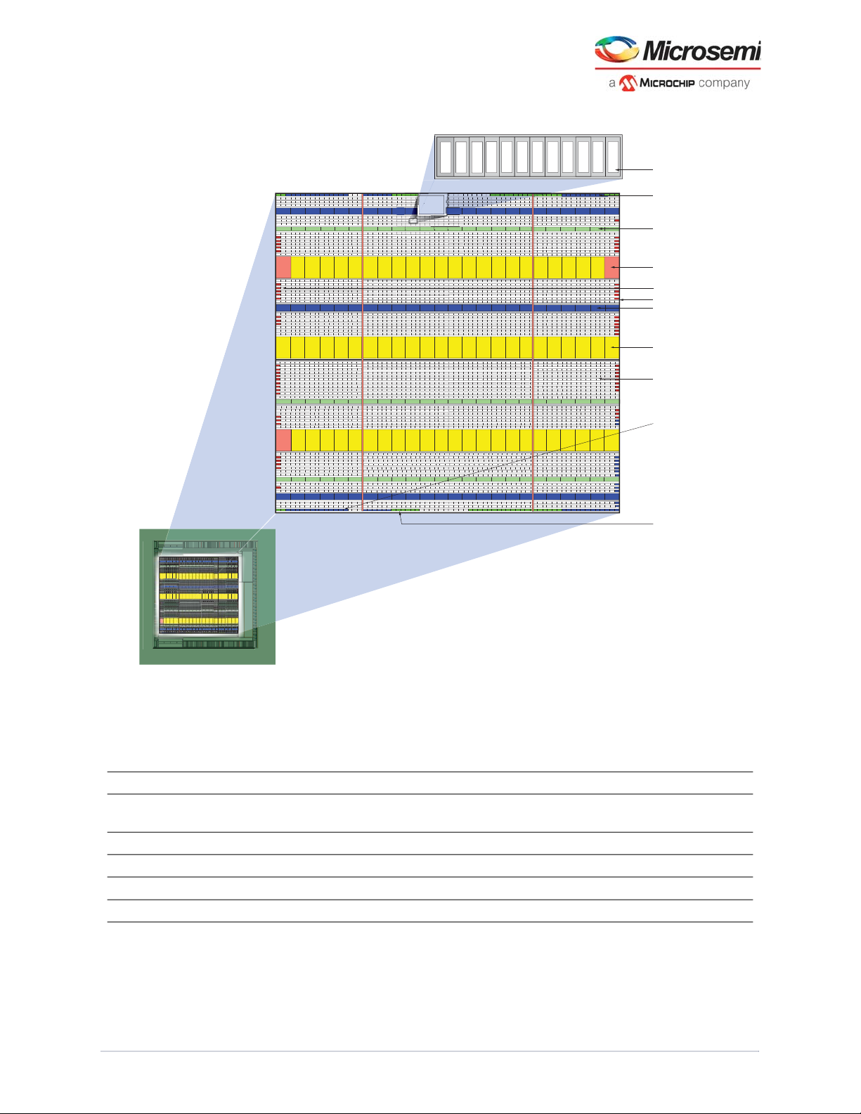
Fabric Architecture
North I/O Clusters
East I/O Clusters
One Logic Element
Chip
Layout
Fabric Layout
One Logic Cluster
South I/O Clusters
West I/O Clusters
Logic Clusters
Mathblocks
LSRAM
uSRAM
CCC(x2)
Interface Clusters
Logic Element
Logic Cluster
Logic Cluster
Lo
Logic Cluster
Lo
Logic
gic Cluster
Logic Element
Logic Element
Logic Element
Logic Element
Logic Element
Logic Element
Logic Element
Logic Element
Logic Element
Logic Element
Logic Element
Figure 1 • SmartFusion2/IGLOO2 Fabric Architecture for M2S050/M2GL050
2.2 Fabric Resources
The following tables list the fabric resources available on SmartFusion2 and IGLOO2 devices.
Table 1 • Fabric Resources for SmartFusion2 Devices
Fabric Resource M2S005 M2S010 M2S025 M2S050 M2S060 M2S090 M2S150
Logic elements
6,060 12,084 27,696 56,340 56,520 86,316 146,124
(4-input LUT + Flip-Flop)
LSRAM 18K blocks 10 21 31 69 69 109 236
µSRAM 1K blocks 11 22 34 72 72 112 240
Math blocks 11 22 34 72 72 84 240
PLLs and CCCs 2 2 6 6 6 6 8
Microsemi Proprietary and Confidential UG0445 User Guide Revision 7.0 4
Page 14
Fabric Architecture
Y
Routing MUXes
LOGIC ELEMENT
LOGIC ELEMENT
S (SUM)
YQ
4-input LUT
with Carry
Chain
ABCD1
D2
EN
CLK
ALDATA
SLDATA
ALDATA
LOGIC ELEMENT
data
C
out
C
in
FF
D
EN
CLK
SLDATA
Q
C
out
C
in
Table 2 • Fabric Resources for IGLOO2 Devices
Fabric Resource M2GL005 M2GL010 M2GL025 M2GL050 M2GL060 M2GL090 M2GL150
Logic elements
6,060 12,084 27,696 56,340 56,520 86,316 146,124
(4-input LUT + FlipFlop)
LSRAM 18K blocks 10 21 31 69 69 109 236
µSRAM 1K blocks 11 22 34 72 72 112 240
Math blocks 11 22 34 72 72 84 240
PLLs and CCCs 2 2 6 6 6 6 8
2.3 Architecture Overview
The following sections of this chapter describe the SmartFusion2 and IGLOO2 fabric architecture in
detail.
• Logic Element
• Interface Logic Element
• I/O Module
• FPGA Routing Architecture
2.3.1 Logic Element
The logic elements can be used as a combinational logic element (CLE), and/or sequential logic element
(SLE) in the design. Each logic element consists of:
• A 4-input LUT
• A dedicated carry chain based on the carry look-ahead technique
• A separate flip-flop which can be used independently from the LUT
The following illustration shows the functional block diagram of the logic element with carry chain.
Figure 2 • Functional Block Diagram of Logic Element
Microsemi Proprietary and Confidential UG0445 User Guide Revision 7.0 5
Page 15

Fabric Architecture
The 4-input LUT can be configured to implement any 4-input combinatorial function or to implement an
arithmetic function, where the LUT output is XORed with carry input (Cin) to generate the sum (S) output.
The sum output, S, is typically used as an output for arithmetic functions but can also be used as an
output for logical functions along with the other output, Y, when the LUT is used to implement
combinatorial functions.
Each logic element has a dedicated 3-bit look-ahead carry implementation, which is used to implement a
dedicated carry chain between the logic elements when the LUT is used to implement arithmetic
operations.
The carry chain has hardwired routing nets running between the logic elements, which reduces the carry
propagation delay through the carry chain, thus giving better performance. The logic element also
contains a dedicated flip-flop, which can be used in conjunction with or independently from the LUT. The
flip-flop can be configured as a register or latch. It has asynchronous and synchronous load and clock
enable inputs. Asynchronous load signal (ALDATA) can be used as asynchronous set or reset signal of
each fabric D flip-flops. It sets or resets the register depending on configuration. Synchronous load signal
(SLDATA) can be used as synchronous set or reset signal of each fabric D flip-flop. It sets or resets the
register depending on configuration. The data input of the flip-flop can be fed from the direct input (D1) or
from the outputs of the 4-input LUT inside the logic element.
2.3.2 Interface Logic Element
Embedded hard blocks (LSRAM blocks, µSRAM blocks, and math blocks) contain a dedicated interface
logic. The embedded hard blocks are connected to the fabric routing structure through LUTs and
flip-flops on their inputs and outputs, and these together form the interface logic element.
Each embedded hard block is associated with 36 interface logic elements. This interface logic element is
structurally equivalent to a logic element but does not have a dedicated carry chain. When a given
embedded hard block is used by the target design, the interface logic is used to connect the embedded
hard block’s I/Os to the fabric routing. If an embedded hard block is not used by the design, the interface
logic element is available for use as a normal logic elements for implementing combinatorial and
sequential circuits. These are in addition to the logic elements available in the fabric.
2.3.3 I/O Module
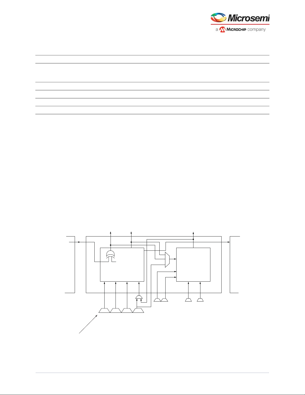
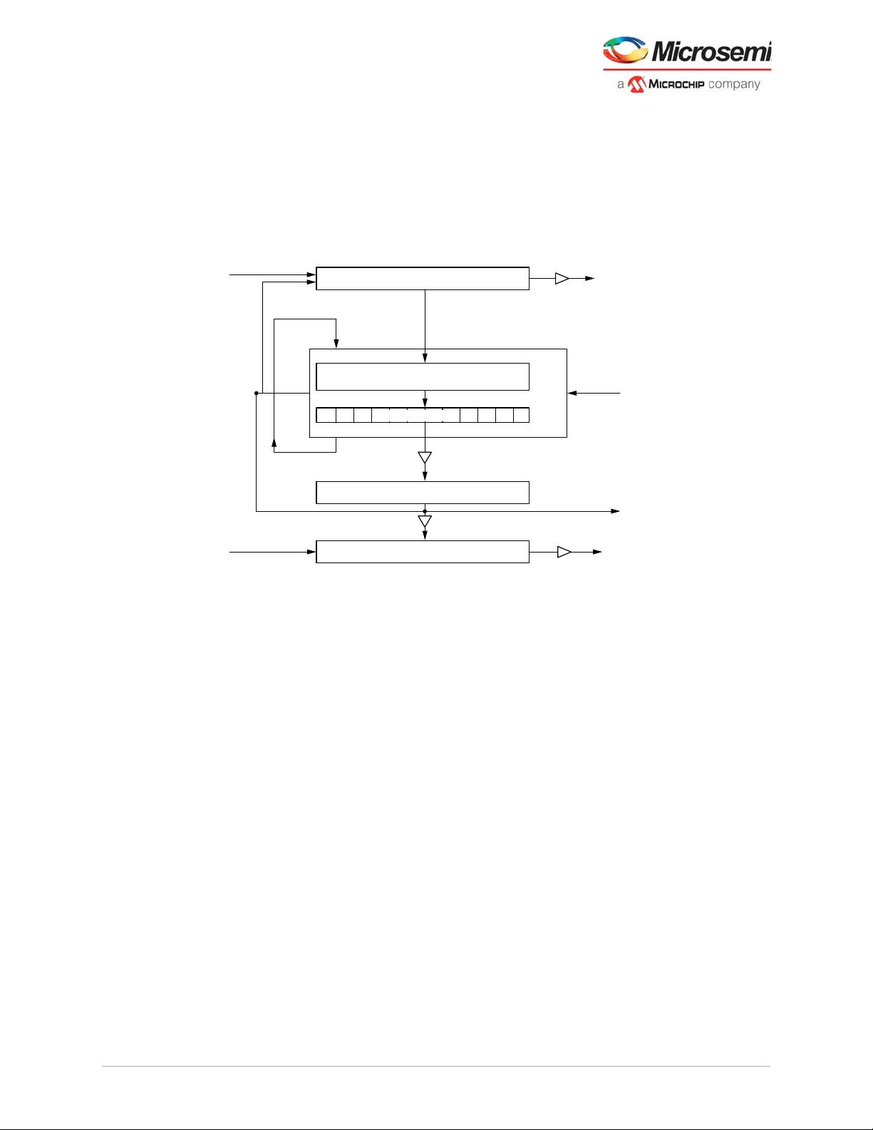
The I/O module includes the I/O digital (IOD) circuitry and the associated routing interface. Each user I/O
pad is connected to its own dedicated I/O module. The I/O module interfaces the user I/Os with the fabric
routing and enables the routing of external signals coming in through the I/Os to reach all the logic
elements. The I/O modules also enable the internal signals to reach the I/Os.
The following illustration shows the functional diagram of the complete MSIO with the IOD and I/O analog
(IOA) sections. The IOD consists of the input registers, output registers, output enable registers, and
routing multiplexers (MUXes). The output register provides the registered version of the output signals to
the I/Os. In the same way, the input registers are used to register the inputs received from the I/Os. The
output enable acts as a control signal for the output, if the I/O is configured as a tristated or bidirectional
I/O. These registers in the I/O modules are similar to the D-flip-flops available in the logic element. The
usage of the output registers in the I/O modules for registering the output signals at I/Os enables better
design performance. Also, in the case of a signal bus, these registers ensure that all the bits of the signal
bus are synchronized to the clock signal when being sent out through the I/Os. At the input side, the input
registers allow capturing the input signals and synchronizing them to the design clock.
Microsemi Proprietary and Confidential UG0445 User Guide Revision 7.0 6
Page 16
Fabric Architecture
Figure 3 • Functional Block Diagram of MSIO
Output data
OCLK
Output enable
Output data
Output enable
non-registered
input data
registered input data
I/O Module (IOD)
ICLK
outreg
outreg
outreg
outreg
inreg
DO_P
OE_P
DO_N
OE_N
DI_P
RX
RX
Weak pull-up/pull-down
resistor control
Differential
ODT
01
PAD_P
PAD_N
V
REF
IOA
TX
ODT
0
1
0
1
TX
ODT
non-registered
input data
registered input data
DI_N
inreg
2.3.4 FPGA Routing Architecture
The SmartFusion2 and IGLOO2 fabric has a clustered routing architecture. Clustering is a hierarchical
grouping of fabric resources that allows a more area-efficient implementation of designs while
maintaining optimal performance. It also helps in reducing the run-time of the place-and-route software.
The SmartFusion2 and IGLOO2 fabric routing architecture is composed of three types of clusters:
• Logic Cluster
• Interface Cluster
• I/O Cluster
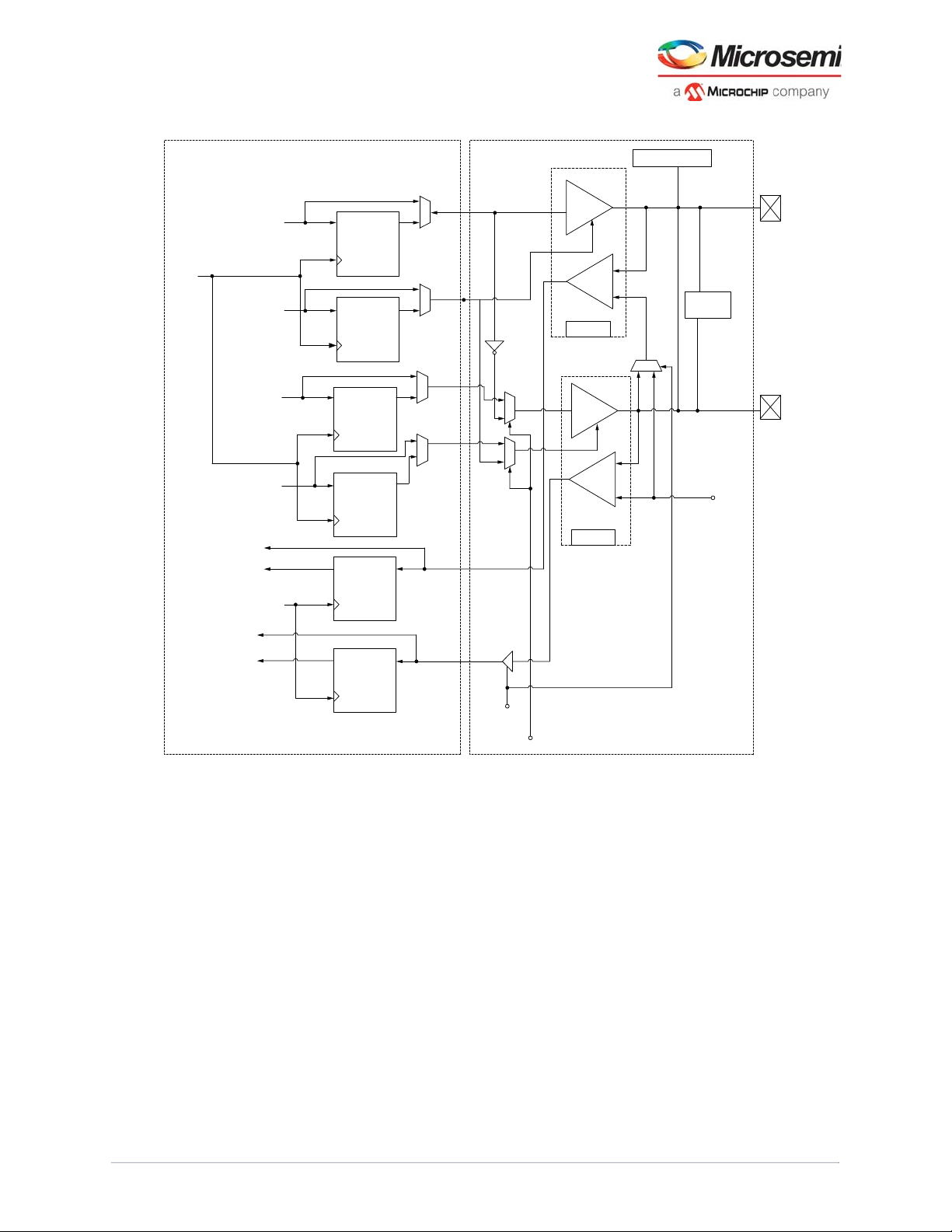
2.3.4.1 Logic Cluster
The logic cluster is a combination of 12 logic elements with a dedicated hardwired carry chain
implemented for all 12 logic elements. The logic clusters contain routing MUXes. Each routed signal is
driven by a unique logic element output or routing MUX. All the logic elements are interconnected with
feedback from outputs to inputs. The intra-routing inside the logic clusters has a very low propagation
delay as compared to the routing outside the logic clusters.
DIFF_IN
DIFF_OUT
Microsemi Proprietary and Confidential UG0445 User Guide Revision 7.0 7
Page 17
Fabric Architecture
Logic Elements
Cluster Carry IN
Cluster Carry Out
Intra-cluster
Routing
Buffers
Dedicated Carry Chain
Interface Cluster
Routing
Interface Cluster
Embedded Hard Blocks-LSRAMs, µSRAMs, Mathblocks, CCCs
3 Clusters Wide
Interface
Logic
LUT+ FF
Routing
Interface
Logic
LUT+ FF
12 Interface Logic 12 Interface Logic
Each LUT, D-flip-flop, and the carry-circuit in the logic cluster have an individual X-Y logical coordinate
assigned, and this makes them independently addressable. The following illustration shows the top-level
logic cluster layout diagram.
Figure 4 • Logic Cluster Top-Level Layout
2.3.4.2 Interface Cluster
The interface cluster is similar to the logic cluster except that it is a combination of 12 interface logic
elements. These clusters are used to interface the inputs and outputs of the embedded hard blocks
(LSRAM, µSRAM, math blocks, and CCCs) to fabric routing. Each embedded hard block is spanned by 3
interface clusters, as shown in the following figure. The interface logic can be used as a logic elements
(without carry chain) when the associated embedded hard block is not used by the design.
Figure 5 • Interface Cluster
2.3.4.3 I/O Cluster
I/O clusters are combinations of I/O modules and the associated routing interfaces. The north and south
I/O clusters each contain four I/O modules. The east and west I/O clusters, each contain three I/O
modules. Each I/O pad is associated with its own dedicated I/O module.
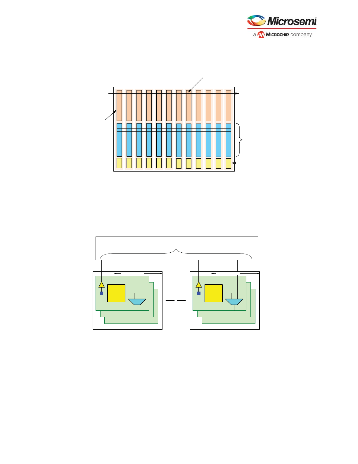
2.3.4.4 Routing Structure
The routing of any design is completed automatically by the software, thus, the utilization of the routing
resources is completely transparent to the user. The selection among various routing resources by the
placement-and-routing software is impacted by the design constraints provided. See SmartFusion2 and
IGLOO2 SmartTime, I/O Editor and ChipPlanner User Guide for more details on how to use the
constraints using Libero SoC software.
Microsemi Proprietary and Confidential UG0445 User Guide Revision 7.0 8
Page 18
Fabric Architecture
Knowledge of the routing architecture and functional modules can be useful in providing effective design
constraints to the software, so that it can be guided to do an optimal design implementation on the
SmartFusion2 and IGLOO2 fabric.
In the SmartFusion2 and IGLOO2 device, the fabric routing is segregated into two parts:
• Inter-cluster routing
• Intra-cluster routing
The following illustration shows the fabric routing structure for the SmartFusion2 and IGLOO2 device.
Figure 6 • Fabric Routing Structure
From Other
Clusters
Inter-Cluster Routing
To Other
Clusters
Cluster
From Adjacent
To Adjacent
To Other
Clusters
Clusters
Clusters
From Other
Clusters
Intra-Cluster Routing (3 Levels of Routing Muxes)
Logic Elements
Output MUXes
Inter-Cluster Routing
Inter-cluster routing spans the clusters and connects them together. The inter-cluster routing resource is
common to all the clusters inside the fabric and is universal across the clusters.
Intra-cluster routing spans the modules that constitute a cluster. Intra-cluster routing is not unique and
varies from cluster to cluster, depending upon the functionality of the cluster. For example, the intracluster routing for an interface cluster is different from that of a logic cluster. There are differences in the
routing of the various interface clusters, depending upon the embedded hard block to which they
interface.
Inter-cluster routing and intra-cluster routing are completely separate. Inter-cluster routing never drives
the inputs of the functional modules (logic elements, interface logic elements, or I/O modules) directly
and the outputs of the functional modules do not drive the inter-cluster routing directly. Inter-cluster
routing has to pass through the intra-cluster routing to reach the functional modules. That makes
SmartFusion2 and IGLOO2 routing a fully clustered routing architecture.
The global network can also drive intra-cluster routing through special routing MUXes. These global
routing MUXes bring in flip-flop control signals such as clock, enable, and sets/resets.
There are a few short routing lines between the adjacent clusters and between the inter-cluster and intracluster routing MUXes. These short paths are provided to provide better performance to the signals
routed through these lines.
Microsemi Proprietary and Confidential UG0445 User Guide Revision 7.0 9
Page 19
Fabric Architecture
2.4 Fabric Array Coordinate System
Every element in the SmartFusion2 and IGLOO2 fabric has individual logical X-Y coordinates associated
with the fabric array coordinate system. These logical coordinates are used by the place-and-route
software while implementing the design using the fabric elements. The place-and-route software can be
constrained to occupy the design components in specific locations inside the fabric using this coordinate
system. Regions can be created inside the fabric and a particular part of the design can be assigned to
that region using the Libero SoC floor-planner software.
The boundaries of these regions can be specified using the array coordinates. Similarly, the embedded
hard block is also addressable through the fabric coordinate system.
The array coordinates are measured from the bottom-left corner to the top-right corner of the FPGA
fabric. Table 3, page 12 provides the array coordinates of logical modules and embedded hard blocks of
SmartFusion2 and IGLOO2 devices. Figure 7, page 10, Figure 8, page 11, and Figure 9, page 11 show
the array coordinates of an M2S050/M2GL050, M2S060/M2GL060, M2S025/M2GL025, and
M2S010/M2GL010 devices. For more information on how to use array coordinates for region/placement
constraints, see Libero SoC User Guide or online help (available in the software) for SmartFusion2 and
IGLOO2 Libero SoC tools.
Figure 7 • M2S050/M2GL050 and M2S060/M2GL060 Fabric Logical Coordinates
(0,206)
LSRAM (36,194)
(887,206)
(851,194)
Mathblocks (0,158)
uSRAM (0,146)
LSRAM (0,134)
Mathblocks (0,95)
uSRAM (0,83)
Mathblocks (0,59)
uSRAM (0,47)
LSRAM (36,11)
(0,0)
(887,158)
(887,146)
(887,134)
(887,95)
(887,83)
(887,59)
(887,47)
(887,11)
(887,0)
Microsemi Proprietary and Confidential UG0445 User Guide Revision 7.0 10
Page 20
Fabric Architecture
(0,146)
Mathblocks (0,110)
uSRAM (0,98)
LSRAM (36,11)
Mathblocks (0,35)
uSRAM (0,23)
LSRAM (36,194)
(635,146)
(635,110)
(635,98)
(635,11)
(635,0)
(635,35)
(635,23)
(599,194)
(0,0)
Figure 8 • M2S025/M2GL025 Fabric Logical Coordinates
Figure 9 • M2S010/M2GL010 Fabric Logical Coordinates
(0,104)
LSRAM (0,92)
Mathblocks (0,80)
uSRAM (0,68)
LSRAM (0,47)
Mathblocks (0,23)
uSRAM (0,11)
(0,0)
(407,104)
(371,92)
(407,80)
(407,68)
(407,47)
(407,23)
(407,11)
(407,0)
Microsemi Proprietary and Confidential UG0445 User Guide Revision 7.0 11
Page 21

Fabric Architecture
Table 3 • Fabric Array Coordinate Systems
Logic Elements µSRAM LSRAM Math Blocks
Min Max Bottom Middle Top Bottom Middle Top Bottom Middle Top
Device
M2S005
M2GL005
M2S010
M2GL010
M2S025
M2GL025
M2S050
M2GL050
M2S060
M2GL060
M2S090
M2GL090
M2S150
M2GL150
X Y X Y (X,Y) (X,Y) (X,Y) (X,Y) (X,Y) (X,Y) (X,Y) (X,Y) (X,Y)
0 0 407 56 NA NA (0,11) NA NA (0,44) NA NA (0,23)
0 0 407 104 (0,11) NA (0,68) (0,47) NA (0,92) (0,23) NA (0,80)
0 0 635 146 (0,23) NA (0,98) (36,11) NA (36,134)(0,35) NA (0,110)
0 0 887 206 (0,47) (0,83) (0,146) (36,11) (0,134) (36,194)(0,59) (0,95) (0,158)
0 0 887 206 (0,47) (0,83) (0,146) (36,11) (0,134) (36,194)(0,59) (0,95) (0,158)
0 0 1031 266 (0, 23) (0, 59)
(0, 194)
0 0 1463 314 (0, 35)
(0, 59)
(0, 107)
(0, 182)
(0, 242) (36, 11) (0, 119)
(0, 170)
(0, 230)
(0, 278)
(36, 11)
(0, 95)
(0, 143)
(0, 218)
(36,
254)
(0, 266)
(36,
302)
(0, 35) (0, 71) (0, 206)
(0, 47)
(0, 71)
(0, 119)
(0, 194)
(0, 242)
(0, 290)
Microsemi Proprietary and Confidential UG0445 User Guide Revision 7.0 12
Page 22

LSRAM
3 LSRAM
3.1 Introduction
The SmartFusion2 and IGLOO2 fabric has embedded 18 Kbit SRAM blocks used for storing data. These
large SRAM blocks (LSRAMs) are arranged in multiple rows within the FPGA fabric and can be
accessed through the fabric routing architecture. The number of LSRAM blocks available depends upon
the specific SmartFusion2 and IGLOO2 device, as shown in the following table. For example, in the
M2S050 or M2GL050 device, there are 69 LSRAM blocks available, which are spread across three rows
inside the fabric.
3.1.1 Features
The SmartFusion2 and IGLOO2 LSRAM blocks have the following features:
• Each LSRAM block can store up to 18,432 bits of data and can be configured in any of the following
depth x width combinations: 512 x 36, 512 x 32, 1k x 18, 1k x 16, 2k x 9, 2k x 8, 4k x 4, 8k x 2, or
16k x 1.
• Each LSRAM block contains two independent data ports—Port A and Port B.
• The LSRAM is synchronous for both read and write operations. These operations are triggered on
the rising edge of the clock.
• Supports maximum frequency up to 400 MHz.
• An optional pipeline register is available at the read data port to improve the clock-to-out delay.
• LSRAM supports two types of read operations:
• Flow-through read (or non-pipelined)
• Pipelined read
• LSRAM supports two types of write operations:
• Simple write
• Feed-through write (write-bypass write)
• LSRAM can be operated in two memory modes:
• Dual-port mode
• Two-port mode
• A write operation requires one clock cycle.
• A read operation requires one clock cycle in Non-pipelined mode. In Pipelined mode, the output data
appears in the next cycle.
• Read from both ports at the same location is allowed.
• Read and write on the same location at the same time is not allowed. There is no built in collision
prevention or detection circuit in LSRAM.
3.2 LSRAM Resources
The following table lists LSRAM rows and 18K blocks available in SmartFusion2 and IGLOO2 devices.
Table 4 • SmartFusion2 and IGLOO2 LSRAM (18Kb Blocks) Resource Table
M2S005/
Device
Rows 1 2 2 3 3 4 6
LSRAM 18 K Blocks 10 21 31 69 69 109 236
Note: All numbers given above are per device.
M2GL005
Microsemi Proprietary and Confidential UG0445 User Guide Revision 7.0 13
M2S010/
M2GL010
M2S025/
M2GL025
M2S050/
M2GL050
M2S060/
M2GL060
M2S090/
M2GL090
M2S150/
M2GL150
Page 23
LSRAM
3.3 Functional Description
This section provides the detailed description of the following:
• Architecture Overview
• Port List
• Port Descriptions
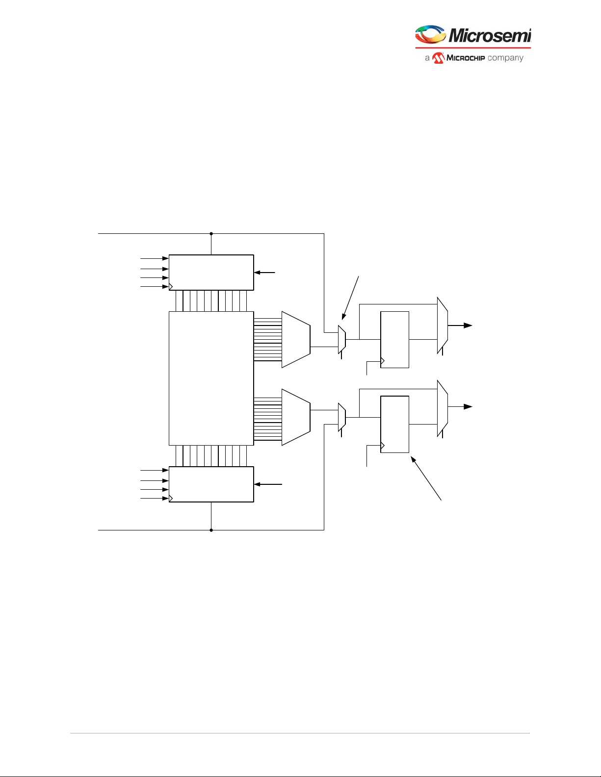
Architecture Overview
SmartFusion2 and IGLOO2 LSRAM embedded memory includes the RAM1Kx18 macro. The following
illustration shows a simplified block diagram of the LSRAM memory block and Table 5, page 15 provides
the port descriptions. The following illustration shows two independent data ports, the pipeline registers
for read data delay, and the feed-through multiplexers to enable immediate access to the write data.
Figure 10 • Simplified Functional Block Diagram for LSRAM
A_ DIN[17 : 0 ]
A_ADDR[13:0 ]
A_WEN[1:0]
A_BLK[2 :0]
A_CLK
B_A DDR[ 13 : 0 ]
B_WEN[ 1: 0]
`
B_BLK[ 2:0 ]
B_C LK
B_ DIN[ 17:0 ]
Port A Row Decode
Write Control
Memory
Array
1K x 18
Port B Row Decode
Write Control
A_ARST_N
Column
Decode
Column
Dec ode
B_A RST_N
A_WMODE
Feed-through MUX
A
_DOUT_CLK
B_WMODE
B_ DOUT_CLK
A_DOUT[17 :0 ]
A_DOUT_LAT
B_DOUT[ 17 : 0]
B_DOUT_LAT
Pipeline Register
Microsemi Proprietary and Confidential UG0445 User Guide Revision 7.0 14
Page 24

LSRAM
3.3.1 Port List
Table 5 • Port List for LSRAM Macro (RAM1KX18)
Port Name Direction Type
PORT A
A_WIDTH[2:0] Input Static Port A Width/depth mode select
A_WEN[1:0]2 Input Dynamic High Port A Write enable
A_ADDR[13:0] Input Dynamic Port A Address input
A_DIN[17:0] Input Dynamic Port A Data input
A_DOUT[17:0] Output Dynamic Port A Data output
A_BLK[2:0] Input Dynamic High Port A Block select
A_WMODE Input Static High Port A Feed-through write select
A_CLK Input Dynamic Rising Port A Clock
A_ARST_N Input Dynamic Low Port A Asynchronous reset
A_DOUT_CLK Input Dynamic Rising Port A Pipeline register clock
A_DOUT_LAT Input Static Low Port A Pipeline register Select
A_DOUT_ARST_N Input Dynamic Low Port A Pipeline register asynchronous reset
A_DOUT_EN Input Dynamic High Port A Pipeline register enable
A_DOUT_SRST_N Input Dynamic Low Port A Pipeline register synchronous reset
PORT B
B_WIDTH[2:0] Input Static Port B Width/depth mode select
B_WEN[1:0]
B_ADDR[13:0] Input Dynamic Port B Address input
B_DIN[17:0] Input Dynamic Port B Data input
B_DOUT[17:0] Output Dynamic Port B Data output
B_BLK[2:0] Input Dynamic High Port B Block select
B_WMODE Input Static High Port B Feed-through write select
B_CLK Input Dynamic Rising Port B Clock
B_ARST_N Input Dynamic Low Port B Asynchronous reset
B_DOUT_CLK Input Dynamic Rising Port B Pipeline register clock
B_DOUT_LAT Input Static Low Port B Pipeline register select
B_DOUT_ARST_N Input Dynamic Low Port B Pipeline register asynchronous reset
B_DOUT_EN Input Dynamic High Port B Pipeline register enable
B_DOUT_SRST_N Input Dynamic Low Port B Pipeline register synchronous reset
Common Signals
A_EN Input Static Low Port A power-down
B_EN Input Static Low Port B power-down
SII_LOCK Input Static High Lock access to SII
BUSY Output Dynamic High Busy signal from SII
2
Input Dynamic High Port B Write enable
1
Polarity Description
1. Static inputs are defined at design time and can be or are controlled by flash configuration bits.
Microsemi Proprietary and Confidential UG0445 User Guide Revision 7.0 15
Page 25

LSRAM
2. If LSRAM is configured in two-port mode with a write data width of x36/x32 and read data width of x36/x32, both the
bits of A_WEN and B_WEN must be tied to logic 1 and should not be dynamically changed.
3.3.2 Port Descriptions
3.3.2.1 A_WIDTH[2:0] and B_WIDTH[2:0]
These signals represent the depth x width mode selections for each port. The following table shows the
depth x width based on ports width selection.
Table 6 • Depth/Width Mode Selection
A_WIDTH/B_WIDTH Depth/Width
000 16K x 1
001 8K x 2
010 4k x 4
011 2K x 9
2K x 8
100 1K x 18
1K x 16
101
110
111
(Two-port)
512 x 36
512 x 32
3.3.2.2 A_WEN[1:0] and B_WEN[1:0]
These signals represent the write enables for each port to select read/write operations. The following
table shows the depth x width operations based on port write enable selection.
Table 7 • Read/Write Operation Selection
Depth x Width A_WEN/B_WEN Operation
16K x 1
8K x 2
4K x 4
2K x 8
2K x 9
1K x 16
1K x 18
16K x 1
8K x 2
4K x 4
2K x 8
2K x 9
1K x 16
1K x 18
512 x 32
(Two-port write-Port B)
512 x 36
(Two-port write-Port B)
1, 2
00 Read
operation
1 Write
operation
A_WEN[1:0] = “11”
B_WEN[1:0] = “11”
B_WEN[1:0] = “11”
A_WEN[1:0] = “11”
Write [31:0]
Write [35:0]
1. In dual-port mode, every port reads when the corresponding write
enable (A_WEN/B_WEN) is "00" and corresponding port select
(A_BLK/B_BLK) is active.
Microsemi Proprietary and Confidential UG0445 User Guide Revision 7.0 16
Page 26

LSRAM
2. In two-port mode, the read port (Port A) reads in every clock cycle if
A_BLK is active.
3.3.2.3 A_ADDR[13:0] and B_ADDR[13:0]
These signals represent the address buses for the two ports. In x1 mode 14 bits are used to address the
16,384 independent locations. In wider modes (x2, x4, etc.) fewer address bits are used. The used
address bits are the most significant bits (MSB). The unused bits are the least significant bits (LSBs) and
they must be grounded. The following table shows the address bus used and unused bits for depth x
width selections.
Table 8 • Address Bus Used and Unused Bits
A_ADDR/B_ADDR
Depth x Width
16K x 1 [13:0] None
8K x 2 [13:1] [0]
4K x 4 [13:2] [1:0]
2K x 9
2K x 8
1K x 18
1K x 16
512 x 36 [13:5] [4:0]
Used Bits Unused bits (to be grounded)
[13:3] [2:0]
[13:4] [3:0]
3.3.2.4 A_DIN[17:0] and B_DIN[17:0]
These signals represent the data input buses for the two ports. In dual-port mode, the data width can
range from 1 bit to 18 bits. In two-port mode, Port B becomes the write-only port. Giving a write data
width of 36 bits, A_DIN[17:0] becomes write data[35:18] and B_DIN[17:0] becomes write data[17:0]. The
used bits for any mode are LSB justified in the data bus and the unused MSB bits must be grounded. The
following table shows the data input buses used and unused bits for depth x width selections.
Table 9 • Data Input Buses Used and Unused Bits
Depth x Width A_DIN/B_DIN
Used Bits Unused bits (to be grounded)
16K x 1 [0] [17:1]
8K x 2 [1:0] [17:2]
4K x 4 [3:0] [17:4]
2K x 8 [7:0] [17:8]
2K x 9 [8:0] [17:9]
1K x 16 [16:9] is [15:8]
[7:0] is [7:0]
1K x 18 [17:0] None
512 x 32 A_DIN[16:9] is [31:24]
A_DIN[7:0] is [23:16]
B_DIN[16:9] is [15:8]
B_DIN[7:0] is [7:0]
[17]
[8]
A_DIN[17]
A_DIN[8]
B_DIN[17]
B_DIN[8]
512 x 36 A_DIN[17:0] is [35:18]
B_DIN[17:0] is [17:0]
Microsemi Proprietary and Confidential UG0445 User Guide Revision 7.0 17
None
Page 27

LSRAM
3.3.2.5 A_DOUT[17:0] and B_DOUT[17:0]
These signals represent the data output buses for the two ports. In dual-port mode, the data width can
range from 1 bit to 18 bits. In two-port mode, Port A becomes the read-only port. Giving a read data width
of 36 bits, A_DOUT[17:0] becomes read data[35:18] and B_DOUT[17:0] becomes read data[17:0]. The
used bits for any mode are LSB justified in the data bus and the unused MSB bits must be unconnected.
The following table shows the data output buses used and unused bits for depth x width selections.
Table 10 • Data Output Buses Used and Unused Bits
A_DOUT/B_DOUT
Depth x Width
16K x 1 [0] [17:1]
8K x 2 [1:0] [17:2]
4K x 4 [3:0] [17:4]
2K x 8 [7:0] [17:8]
2K x 9 [8:0] [17:9]
1K x 16 [16:9] is [15:8]
1K x 18 [17:0] None
512 x 32 A_DOUT[16:9] is [31:24]
512 x 36 A_DOUT[17:0] is [35:18]
Used Bits Unused bits (unconnected)
[7:0] is [7:0]
A_DOUT[7:0] is [23:16]
B_DOUT[16:9] is [15:8]
B_DOUT[7:0] is [7:0]
B_DOUT[17:0] is [17:0]
[17]
[8]
A_DOUT[17]
A_DOUT[8]
B_DOUT[17]
B_DOUT[8]
None
3.3.2.6 A_BLK[2:0] and B_BLK[2:0]
These signals represent the port select control signals for each port. The following table shows
operations (Read, Write, and No operation) based on selection of port select control signals.
Table 11 • Port Select Control Signals
Port Select Signal Value Result
A_BLK[2:0] 111 Perform read or write operation on Port A.
A_BLK[2:0] 000
001
010
011
100
101
110
B_BLK[2:0] 111 Perform read or write operation on Port B.
B_BLK[2:0] 000
001
010
011
100
101
110
No operation in memory from Port A. Port A output is forced to logic 0.
No operation in memory from Port B. Port B output is forced to logic 0.
Microsemi Proprietary and Confidential UG0445 User Guide Revision 7.0 18
Page 28

LSRAM
3.3.2.7 A_WMODE and B_WMODE
These signals represent the Write mode control signals for Port A and Port B.
• Logic 0: Output data port holds the previous value.
• Logic 1: Feed-through; write data appears on the corresponding output data port. In two-port mode,
feed-through write is not supported.
3.3.2.8 A_CLK and B_CLK
These signals represent the clock inputs for Port A and Port B. All inputs must be set up before the rising
edge of the clock. The read or write operation begins with the rising edge.
3.3.2.9 A_ARST_N and B_ARST_N
These signals represent Active Low, asynchronous reset inputs for Port A and Port B. Assertion of these
resets during read operation forces the data output lines to logic 0. Assertion of these resets during write
operation results in garbage values written into the memory.
3.3.2.10 A_DOUT_ARST_N and B_DOUT_ARST_N
These signals represent Active Low, asynchronous reset inputs for the output pipeline registers for Port A
and Port B. Assertion of these reset signals forces the data output to logic 0. In Non-pipelined mode,
these inputs should be tied to logic 1.
3.3.2.11 A_DOUT_LAT and B_DOUT_LAT
These signals represent Latch mode inputs for the output pipeline registers for Port A and Port B.
• Logic 0: Register operation
• Logic 1: Latch operation
3.3.2.12 A_DOUT_EN and B_DOUT_EN
These signals represent Active High; enable inputs for the output pipeline registers for Port A and Port B.
• Logic 1: Normal register operation
• Logic 0: Register holds previous data
3.3.2.13 A_DOUT_SRST_N and B_DOUT_SRST_N
These signals represent Active Low, synchronous reset inputs for the output pipeline registers for Port A
and Port B. Assertion of these reset signals forces the data output to logic 0. In Non-pipelined mode,
these inputs should be tied to logic 1.
3.3.2.14 A_EN and B_EN
These are Active Low, power-down configuration bits for each port.
3.3.2.15 SII_LOCK
This control signal, when asserted to logic 1, locks the entire LSRAM memory for being accessed by the
system controller interface bus (SII). The system controller can access the LSRAM for the following
purposes:
• Testing the memory
• Moving data between LSRAM and embedded nonvolatile memory (eNVM) or external memories
• Moving data between various LSRAMs or between µSRAMs and LSRAMs
• LSRAMs cannot be accessed when the system controller is accessing them
3.3.2.16 BUSY
This signal acts as a Status signal when the system controller is accessing the particular LSRAM. Logic
1 on this signal indicates system controller access. This signal can be used to monitor the completion of
LSRAM access.
Microsemi Proprietary and Confidential UG0445 User Guide Revision 7.0 19
Page 29
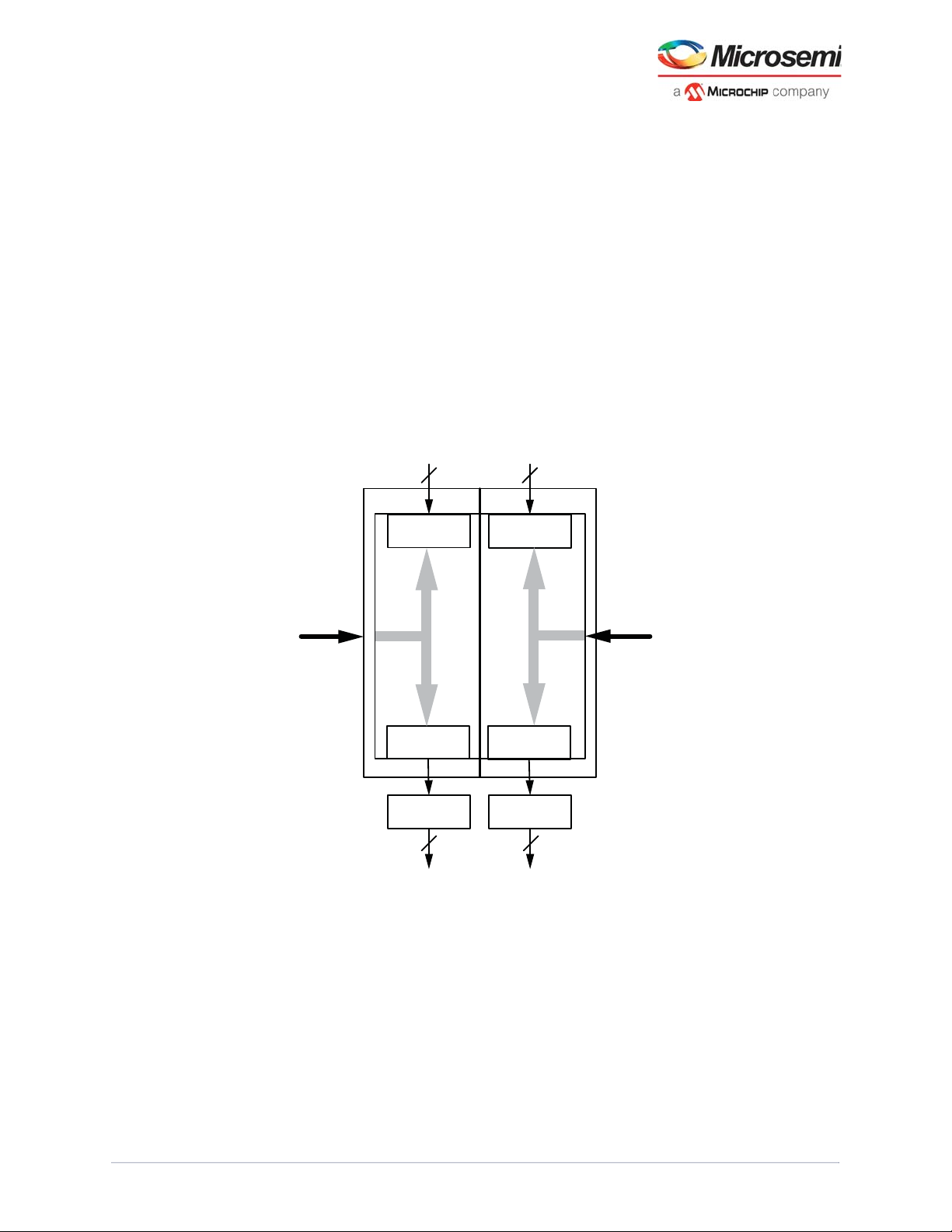
LSRAM
3.4 Memory Modes
LSRAM can be configured as a dual-port SRAM or two-port SRAM.
3.4.1 Dual-Port Mode
LSRAM configured as dual-port SRAM provides a data storage capability of 18 Kbits with two
independent access ports: Port A and Port B, as shown in the following illustration. Read and write
operations can be done from both the ports independently at any location as long as there is no collision.
In dual-port mode, the maximum data width can be x18 for either port. In dual-port mode, each port of the
LSRAM can be configured in the following depth x width configurations:
• 1k x 18, 1k x 16
• 2k x 9, 2k x 8
• 4k x 4
• 8k x 2
• 16k x 1
The following illustration shows the data path for the dual-port SRAM (DPSRAM).
Figure 11 • Data Path for Dual-Port Mode
PORT A
A_DIN B_DIN
18
18
PORT B
DATA In A DATA In B
Port A
Signals
DATA Out A DATA Out B
Pipeline
Register A
18 18
Data can be written to either or both ports and also can be read from either or both ports. Each port has
its own address, data in, data out, clock, block select, and write enable. The read and write operations
are synchronous and require a clock edge.
There is no collision detection or prevention circuit built into LSRAM. Simultaneous write operations from
both the ports to the same address location result in data uncertainty. Simultaneous read and write
operations from both the ports to the same address location results in correct data written into the
memory but garbage values being read out.
Pipeline
Register B
B_DOUTA_DOUT
Port B
Signals
The read operation requires one clock cycle in Non-pipelined mode. In Pipelined mode, the output data
appears in the next cycle. The write operation requires one clock cycle.
Microsemi Proprietary and Confidential UG0445 User Guide Revision 7.0 20
Page 30
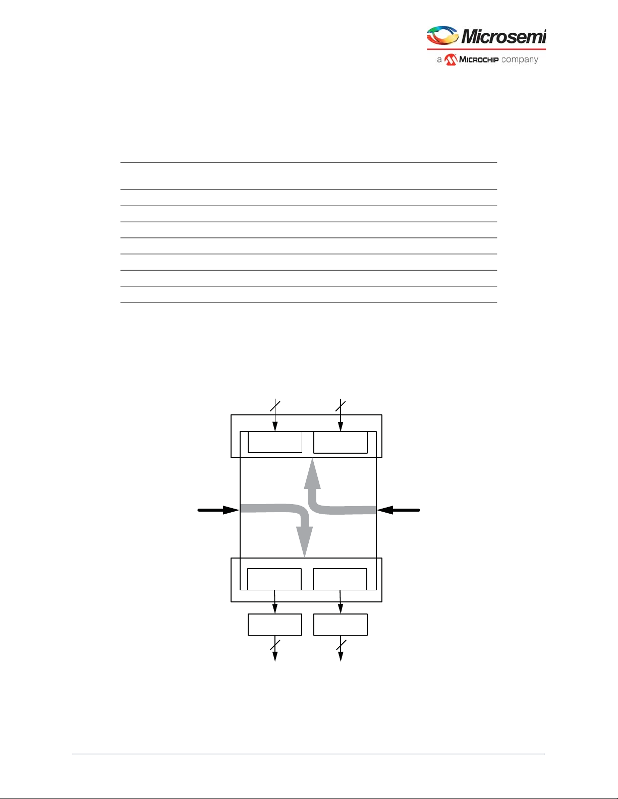
LSRAM
When the read operation is configured with output pipeline registers, the input clock sourcing the pipeline
registers has to be synchronized to the LSRAM's clock input; that is, A_DOUT_CLK should be
synchronized to A_CLK and B_DOUT_CLK should be synchronized to B_CLK.
The following table describes the data width configurations that are supported by LSRAM configured in
dual-port mode.
Table 12 • Data Width Configurations for LSRAM in Dual-Port Mode
Port A Data Width (represented
as “x number of bits”) Port B Data Width (represented as “x number of bits”)
x1 x1, x2, x4, x8, x16
x2 x1, x2, x4, x8, x16
x4 x1, x2, x4, x8, x16
x8 x1, x2, x4, x8, x16
x16 x1, x2, x4, x8, x16
x9 x9, x18
x18 x9, x18
3.4.2 Two-Port Mode
LSRAM configured as two-port SRAM provides a data storage capability of 18 Kbits, with Port A
dedicated to read operations and Port B dedicated to write operations, as shown in the following figure.
In two-port mode, the maximum data width for the read port (Port A) and the write port (Port B) is x36.
Figure 12 • Data Path for Two-Port Mode
PORT A
Port A
Signals
PORT B
A_DIN B_DIN
18
DATA In A DATA In B
DATA Out A DATA Out B
Pipeline
Register A
18 18
18
Pipeline
Register B
B_DOUTA_DOUT
Port B
Signals
Microsemi Proprietary and Confidential UG0445 User Guide Revision 7.0 21
Page 31

LSRAM
In two-port mode, LSRAM can be configured in the following depth x width configurations:
• 512 x 36
• 512 x 32
• 1k x 18, 1k x 16
• 2k x 9, 2k x 8
• 4k x 4
• 8k x 2
• 16k x 1
There is no collision detection or prevention circuit built into LSRAM. Simultaneous read operations from
Port A and write operations from Port B for the same address location should be avoided. This situation
results in correct values being written into the memory, but garbage values will be read out from the
memory.
When the read port data width is configured as x36/x32:
• Output data pins are borrowed from Port B, with Port A forming the MSB and Port B forming the
LSB.
• Input data pins are borrowed from Port A, with Port A forming the MSB and Port B forming the LSB.
The read operation requires one clock cycle in Non-pipelined mode. In Pipelined mode, the output data
appears in the next cycle. The write operation requires one clock cycle.
When the read operation is configured with output pipeline registers, the input clock sourcing the pipeline
registers has to be synchronized to the LSRAM's clock input. When the read data width is x18 or less,
A_DOUT_CLK has to be synchronized to A_CLK. When the read data width is x36/x32, both
A_DOUT_CLK and B_DOUT_CLK have to be synchronized to A_CLK.
Note: Enable pipeline mode to achieve high performance. This will pipeline the output data bus before the data
bus is delivered to the FPGA fabric.
The following table describes the data width configurations supported by LSRAM configured in two-port
mode.
Table 13 • Data Width Configurations for LSRAM in Two-Port Mode
Read Port – Port A (represented
as “x number of bits”) Write Port – Port B (represented as “x number of bits”)
x1 x1, x2, x4, x8, x16
x2 x1, x2, x4, x8, x16
x4 x1, x2, x4, x8, x16
x8 x1, x2, x4, x8, x16
x9 x9, x18
x16 x1, x2, x4, x8, x16
x18 x9, x18
x32 x1, x2, x4, x8, x16, x32
x36 x9, x18, x36
In two-port mode, if the write data width is x36/x32 and read data width is x36/x32, both the bits of
A_WEN and B_WEN have to be tied to logic 1 and should not be dynamically changed.
Microsemi Proprietary and Confidential UG0445 User Guide Revision 7.0 22
Page 32

LSRAM
3.5 Operating Modes
3.5.1 Read Operation
3.5.1.1 Flow-Through Read
Flow-through mode indicates a non-pipelined read operation where the pipeline registers are bypassed
and the data is displayed on the corresponding output in the same clock cycle. During flow-through read
operation, the LSRAM can generate glitches on the data output buses. Therefore, Microsemi
recommends using LSRAM with pipeline registers to avoid these read glitches.
3.5.1.2 Pipelined Read
In a pipelined read operation, the output data is registered at the pipeline registers, so the data is
displayed on the corresponding output in the next clock cycle. In Pipeline mode, pipeline clock input and
LSRAM's clock input should be synchronized and fed with a single clock source.
Microsemi Proprietary and Confidential UG0445 User Guide Revision 7.0 23
Page 33

LSRAM
t
t
tt
tt
t
tt
t
A_CLK
B_CLK
A_ADDR [13:0]
B_ADDR [13:0]
A_BLK [2:0]
B_BLK [2:0]
A_WEN
B_WEN
A_DOUT [17:0] (Non-Pipeline Read)
B_DOUT [17:0] (Non-Pipeline Read)
A_DOUT_CLK
B_DOUT_CLK
A_DOUT_EN
B_DOUT_EN
t
tt
t
t
t
t
t
A_DOUT [17:0] (Pipeline Read)
B_DOUT [17:0] (Pipeline Read)
CY
CL
CH
ADDRSU
ADDRHD
BLKHDBLKSU
RDEHDRDESU
CLK2Q
PLCY
PLCLKMPWH PLCLKMPWL
RDPLESU
RDPLEHD
RDPLEHD
RDPLESU
CLK2Q
3.5.1.3 Timing Diagram: Flow-Through Read and Pipeline Read
• The addresses (A_ADDR, B_ADDR), BLK enables (A_BLK, B_BLK), and read enables (A_WEN,
B_WEN = '0') should be set up before the rising edge of the clock (A_CLK, B_CLK).
• For non-pipeline read operations, data comes on the output bus (A_DOUT, B_DOUT) after a delay
of T
• For pipeline read operations, the data is displayed on the output in the next clock cycle.
The following illustration shows the timing diagram for a read operation performed on LSRAM.
Figure 13 • Read Operation Timing Waveforms
(read access time without pipeline register) in the same cycle.
CLK2Q
Table 14 • Read Operation Timing Parameters
Parameters Description
T
CY
T
CH
T
CL
T
ADDRSU
T
ADDRHD
T
BLKSU
T
BLKHD
T
RDESU
T
RDEHD
Microsemi Proprietary and Confidential UG0445 User Guide Revision 7.0 24
Clock period
Clock minimum pulse width High
Clock minimum pulse width Low
Address setup time
Address hold time
Block select setup time (With pipeline register enabled)
Block select hold time (With pipeline register enabled)
Read enable setup time (A_WEN, B_WEN =0)
Read enable hold time (A_WEN, B_WEN =0)
Page 34

LSRAM
SRAM
Clock2
REnable
Synchronizer
RADDR
Generator
Clock1
Table 14 • Read Operation Timing Parameters (continued)
Parameters Description
T
CLK2Q
Read access time with pipeline register
Read access time without pipeline register
T
PLCY
T
PLCLKMPWH
T
PLCLKMPWHL
T
RDPLESU
Pipelined clock period
Pipelined clock minimum pulse width High
Pipelined clock minimum pulse width Low
Pipelined read enable setup time (A_DOUT_EN,
B_DOUT_EN)
T
RDPLEHD
Pipelined read enable hold time (A_DOUT_EN,
B_DOUT_EN)
Note: Data in the SRAM can be corrupted during a read operation when the read address does not meet setup
and hold requirements with respect to the clock for that port.The data corruption occurs when the read
address (RADDR) changes almost simultaneously with read clock (RCLK) i.e RADDR violates the timing
requirement of the memory.
To avoid data corruption due to Asynchronous clocking for read address and read clock of the RAM,
users must implement a proper synchronizer circuit. The following figure illustrates a sample
Synchronizer mechanism.
Figure 14 • RADDR Synchronizer
3.5.2 Write Operation
3.5.2.1 Feed-Through Write (write-bypass write)
During this write operation, the data written into the memory array is displayed immediately on the
corresponding data output for non-pipeline operation. For pipeline operation data output displays in next
clock. The feed-through write option is not supported when the LSRAM is configured in two-port mode.
3.5.2.2 Simple Write
In simple write, the data written into the memory array is not displayed on the corresponding data output
until it is read out. The data output retains the last read data value.
3.5.2.3 Timing Diagram: Feed-Through Write and Simple Write
• The addresses (A_ADDR, B_ADDR), BLK enables (A_BLK, B_BLK), and write enables (A_WEN,
B_WEN = '1') should be set up before the rising edge of the clock (A_CLK, B_CLK).
• For a feed-through write, the written data is displayed on the output (A_DOUT, B_DOUT) after a
delay of T
• For a simple write, the written data is displayed on the output only when a read operation is
performed on the same address.
in the same clock cycle.
CLK2Q
Microsemi Proprietary and Confidential UG0445 User Guide Revision 7.0 25
Page 35

LSRAM
tt
tt
tt
t
tt
t
A_CLK
B_CLK
A_AADR [13:0]
B_AADR [13:0]
A_BLK [2:0]
B_BLK [2:0]
A_WEN
B_WEN
A_DOUT [17:0] (Feed Through)
B_DOUT [17:0] (Feed Through)
tt
A_DIN [17:0]
B_DIN [17:0]
CY
CH
CL
ADDRSU
ADDRHD
BLKHDBLKSU
WEHD
WESU
DHD
DSU
CLK2Q
The following illustration shows the timing diagram for a write operation performed on LSRAM.
Figure 15 • Write Operation Timing Waveforms
Table 15 • Write Operation Timing Parameters
Parameters Description
T
CY
T
CH
T
CL
T
ADDRSU
T
ADDRHD
T
BLKSU
T
BLKHD
T
WESU
T
WEHD
T
DSU
T
DHD
T
CLK2Q
Microsemi Proprietary and Confidential UG0445 User Guide Revision 7.0 26
Clock period
Clock minimum pulse width High
Clock minimum pulse width Low
Address setup time
Address hold time
Block select setup time (With pipeline register
enabled)
Block select hold time (With pipeline register
enabled)
Write enable setup time (A_WEN, B_WEN =1)
Write enable hold time (A_WEN, B_WEN =1)
Data setup time
Data setup time
Read access time with Feed-through write timing
Page 36

LSRAM
t
t
t
A_CLK
B_CLK
A_ARST_N
B_ARST_N
A_DOUT
B_DOUT
t
CY
CL
CH
R2Q
3.5.3 Reset Operation
The reset signals (A_ARST_N and B_ARST_N) are asynchronous Active Low signals. For any normal
operation of LSRAM, these reset signals should be kept High. To reset the LSRAM, the reset signals
must be Low.
When reset is asserted (A_ARST_N or B_ARST_N forced Low), the LSRAM behaves as follows during
read and write operations:
1. Read operation: If reset is asserted when the read operation is in process, the data output port is
forced Low after a certain amount of delay. If the clock is High and the reset signal is asserted and
then deasserted in the same High clock phase or Low clock phase, the data output stays Low until
the next cycle. The data output changes its state only if a read operation or write operation in Bypass
mode is performed on the LSRAM. In a simple write operation, the data output stays Low.
2. Write operation: The corrupted data is written into the memory. Therefore, Microsemi recommends
to avoid asserting reset during write operation.
3.5.3.1 Timing Diagram: Asynchronous Reset Operation
Figure 16 • Asynchronous Reset Operation
Table 16 • Asynchronous Reset Timing Parameters
Parameters Description
T
T
T
T
CY
CH
CL
R2Q
Clock period
Clock minimum pulse width High
Clock minimum pulse width Low
Asynchronous reset to output propagation delay
3.5.4 Block Select Operation
The block select in LSRAM works like a chip select. When the block select (A_BLK and B_BLK) is High,
the LSRAM is active and read and write operations can be performed.
If the block select is Low, the LSRAM does not perform any read or write operations. It drives logic 0 on
the data output pins until the next read cycle or write operation in Bypass mode. When the pipeline
registers are used, the block select effect at the output is delayed by one pipeline clock cycle (the
pipeline registers are independent of block select).
Microsemi Proprietary and Confidential UG0445 User Guide Revision 7.0 27
Page 37

LSRAM
t
A_CLK
B_CLK
A_BLK [2:0]
B_BLK [2:0]
t
t
A_DOUT [17:0] (Non-Pipeline Mode)
B_DOUT [17:0] (Non-Pipeline Mode)
t
A_DOUT [17:0] (Pipeline Access)
B_DOUT [17:0] (Pipeline Access)
t
t
CY
BLKMPW
BLKHD
BLKSU
BLK2Q
CLK2Q
The following illustration shows the timing diagram for block select inputs for LSRAM.
Figure 17 • Block Select Timings
Table 17 • Block Selection Timing Parameters
Parameters Description
T
CY
T
CH
T
CL
T
BLKSU
T
BLKHD
T
BLKMPW
T
BLK2Q
T
CLK2Q
Clock period
Clock minimum pulse width High
Clock minimum pulse width Low
Block select setup time (with pipeline register enabled)
Block select hold time (with pipeline register enabled)
Block select minimum pulse width
Block select to out disable time (when pipeline registers are disabled)
Read access time without pipeline register
Figure 16, page 27 shows the timing diagram for asynchronous reset operation performed on LSRAM.
Microsemi Proprietary and Confidential UG0445 User Guide Revision 7.0 28
Page 38

LSRAM
3.5.5 Collision
Collision scenarios arise between both ports of the LSRAM when a read operation is requested from one
port and a write operation from the other port simultaneously on the same address location, or when a
write operation occurs at the same location at the same time from both the ports. The following table
describes the behavior of the LSRAM during the various cases of collisions.
Table 18 • Collision Operation Description
Operation Description
Simultaneous read from Port A and
Port B at the same location
Simultaneous read from Port A and
write from Port B at the same
location
Simultaneous read from Port B and
write from Port A at the same
location
Simultaneous write from Port A and
Port B at the same location
Operation is allowed without any restrictions and data is available on the output
ports after the specified time, as described in the read timing diagrams in
Figure 13, page 24.
Not allowed. If the user does this, the new data will be written, but the output data
will be corrupted.
Not allowed. If the user does this, the new data will be written, but the output data
will be corrupted.
Not allowed. If the data to be written is same on both the ports, then data is
successfully written. If the data is different, then the LSRAM cell has an
undetermined state.
There are no collision prevention or detection techniques available in LSRAM. The last 3 scenarios
mentioned in the preceding table are not allowed on LSRAM and should be avoided.
3.6 How to Use LSRAM
The following sections describe how to use LSRAM in an application:
• Design Flow
• LSRAM Use Model
3.6.1 Design Flow
Libero SoC software provides separate configuration tools for dual-port mode and two-port mode. Using
these configuration tools, LSRAM blocks can be configured in the required operating modes. These
configuration tools generate the required HDL wrapper files for LSRAM with appropriate values assigned
to the static signals. The generated LSRAM wrapper HDL files can be used in the design hierarchy by
connecting the ports to the rest of the design.
3.6.1.1 LSRAM Dual-Port Mode
The following illustration shows the ports of the DPSRAM IP macro available in Libero SoC. See
SmartFusion2 Dual-Port Large SRAM Configuration for detailed software configuration information on
dual-port LSRAM.
Microsemi Proprietary and Confidential UG0445 User Guide Revision 7.0 29
Page 39

LSRAM
Figure 18 • Ports of the LSRAM Configured as Dual-Port SRAM - DPSRAM Macro in Libero SoC
tcy
A_CLK
B_CLK
tblkm pw
tblksu
tblkhd
A_ B LK [ 2 :0 ]
B_ B LK [ 2 :0 ]
tblk 2q
A _DOUT [ 17: 0] ( non pipeline mode )
B _DOUT [ 17: 0] ( non pipeline mode )
tclk 2q
A_DOUT [17:0 ] (pipeline access)
B_DOUT [17:0 ] (pipeline access)
Table 19 • Port Description for the DPSRAM Macro
Port Name Direction Description
A_CLK, B_CLK Input These signals represent the clock inputs for Port A and Port B. The same clock
inputs also act as clock inputs for the output pipeline registers if configured as
registers. All inputs must be set up before the rising edge of the clock. The read
or write operation begins with the rising edge.
A_ADDR, B_ADDR Input These signals represent the address inputs for Port A and Port B.
A_BLK, B_BLK Input These signals represent the block-select inputs for Port A and Port B.
A_DIN, B_DIN Input These signals represent the data inputs for Port A and Port B.
A_WEN, B_WEN Input These signals represent the write enables for Port A and Port B.
A_DOUT, B_DOUT Output These signals represent the data outputs for Port A and Port B.
A_DOUT_EN,
Input These signals represent the Read data register Enable for Port A and Port B
B_DOUT_EN
A_DOUT_SRST_N,
B_DOUT_SRST_N
A_DOUT_ARST_N,
B_DOUT_ARST_N
Input These signals represent the Read data register Synchronous reset for Port A
and Port B
Input These signals represent the Read data register Asynchronous reset for Port A
and Port B
Microsemi Proprietary and Confidential UG0445 User Guide Revision 7.0 30
Page 40

LSRAM
3.6.1.2 LSRAM Two-Port Mode
The following figure shows the ports of the TPSRAM IP macro available in Libero SoC. See
SmartFusion2 Two-Port Large SRAM Configuration document for detailed software configuration
information for two-port LSRAM.
Figure 19 • Ports of the LSRAM Configured as Two-Port SRAM - TPSRAM Macro in Libero SoC
Table 20 • Port Description for the TPSRAM Macro
Port Name Direction Description
WCLK Input This signal represents the clock input for the write port (Port B). All write inputs must be
set up before the rising edge of the clock. The write operation begins with the rising
edge.
RCLK Input This signal represents the clock input for the read port (Port A). The same clock inputs
also act as clock inputs for the output pipeline registers if configured as registers. All
read inputs must be set up before the rising edge of the clock. The read operation
begins with the rising edge.
ARST_N Input This signal represents Active Low, asynchronous reset inputs for Port A and Port B.
Assertion of this reset during a read operation forces the data output lines to logic '0'.
Assertion of these resets during a write operation results in garbage values written into
the memory.
WADDR Input This signal represents the address input for write Port B.
RADDR Input This signal represents the address input for read Port A.
WEN Input This signal represents the write enable for write Port B.
WD Input This signal represents the data input for write Port B.
REN Input This signal represents the read enable for read Port A.
RD Output This signal represents the data output for read Port A.
RD_EN Input This signal represents the Read data register enable.
RD_SRST_N Input This signal represents the Read data register Synchronous reset.
Microsemi Proprietary and Confidential UG0445 User Guide Revision 7.0 31
Page 41

LSRAM
3.6.1.3 LSRAM Macro (RAM 1Kx18)
Libero SoC can be used to instantiate the LSRAM macro (RAM1Kx18) in the design. When using the
RAM1Kx18 macro, care should be taken to provide appropriate values to the static signals to configure
the LSRAM correctly before instantiating it in the design.
The following figure shows the LSRAM macro RAM1Kx18 available in Libero SoC.
Figure 20 • RAM1Kx18 Macro
3.6.1.4 Associated LSRAM IP Cores
In addition to LSRAM macros, Libero SoC also has IP cores available to access the LSRAM through
AHB and APB slave interfaces through which configuration parameters such as bus (AHB/APB) data
width, RAM selection (LSRAM and µSRAM), and depth of the memory can be set. Figure 21, page 32
and Figure 22, page 33 show CoreAHBLSRAM and CoreAPBLSRAM, available in the Libero SoC
catalog.
3.6.1.4.1 CoreAHBLSRAM
The following image shows CoreAHBLSRAM IP (LSRAM with AHB slave Interface), available in Libero
SoC. See CoreAHBLSRAM Handbook for detailed software configuration information for dual-port
LSRAM.
Figure 21 • CoreAHBLSRAM IP in Libero SoC
Microsemi Proprietary and Confidential UG0445 User Guide Revision 7.0 32
Page 42

LSRAM
Table 21 • Port Description for the CoreAHBLSRAM IP
Port Name Direction Description
HCLK Input AHB clock. All AHB signals inside the block are clocked on the rising edge.
HRESETn Input AHB Reset. The signal is Active Low. Asynchronous assertion and synchronous
deassertion. Used to reset AHB registers in the block.
S Input/Output AHB slave interface signals include:
HSEL: AHBL slave select
HADDR: AHBL address
HWRITE: AHBL write
HREADYIN: AHBL ready input
3.6.1.4.2 CoreAPBLSRAM
The following figure shows CoreAPBLSRAM IP (LSRAM with APB slave interface), available in Libero
SoC. See CoreAPBLSRAM Handbook for detailed software configuration information.
Figure 22 • CoreAPBLSRAM IP in Libero SoC
Table 22 • Port Description for the CoreAPBLSRAM IP
Port Name Direction Description
PCLK Input APB clock. All APB signals inside the block are clocked on the rising edge.
PRESETn Input APB Active Low asynchronous reset.
S Input/Output APB Slave interface signals include:
PSEL: APB slave select
PADDR: APB Address
PWDATA: APB write data
PRDATA: APB read data
PENABLE: APB strobe. Indicates the second cycle of an APB transfer.
PWRITE: APB write
PREADY: APB3 ready signal for future APB3 compliance. Used to extend APB
transfer.
PSLVERR: APB slave error. Indicates transfer failure. It is tied to Low.
3.6.1.4.3 CoreFIFO IP
Libero SoC IP catalog has a CoreFIFO IP, which can be configured as a soft FIFO for generation of FIFO
control logic. Memory configuration can be selected as LSRAM, µSRAM, or external memory as per the
design requirements. See CoreFIFO Handbook for detailed software configuration information.
Microsemi Proprietary and Confidential UG0445 User Guide Revision 7.0 33
Page 43

LSRAM
3.6.2 LSRAM Use Model
3.6.2.1 Use Model 1: Two-Port SRAM with a Write Data Width of x36 and Read Data
Width of x18
LSRAM does not support any two-port configurations with a write port (Port B) data width of x36/x32 and
a read port (Port B) data width of x18/x9/x8/x4/x2/x1. If such a configuration is required for the design,
two LSRAM blocks must be used to implement these configurations.
Following use model explains how to implement a two-port SRAM (using RAM1Kx18 macros) with a
write data width of x36 and a read data width of x18.
The implementation has the following configurations:
• Write port: 512 x 36
• Read port: 1024 x 18
• Read and write input clock: Two different clock sources
• Pipelined read mode: Disabled
Microsemi Proprietary and Confidential UG0445 User Guide Revision 7.0 34
Page 44

LSRAM
A_CLK
A_ARST_N
A_BLK[2:0]
A_ADDR[13:0]
A_DIN [17:0]
A_WEN[1:0]
A_DOUT_EN
A_DOUT_ARST_N
A_DOUT_SRST_N
B_CLK
B_ARST_N
B_BLK[2:0]
B_ADDR[13:0]
B_DIN [17:0]
B_WEN[1:0]
B_DOUT_EN
B_DOUT_ARST_N
B_DOUT_SRST_N
A_DOUT_LAT
A_WIDTH[2:0]
A_WMODE
A_EN
B_DOUT_LAT
B_WIDTH[2:0]
B_WMODE
B_EN
S_LOCK
A_DOUT[17: 0]
B_DOUT[17: 0]
BUSY
LSRAM #1
LSRAM #2
RCLK
{‘1’}
{REN,’1',’1'}
{‘0’,RADDR[9:0],‘0’,’0',’0'}
{18'b0}
{“00”}
{‘1’}
ARST_N
{‘1’}
WCLK
A_DOUT_CLK
{‘1’}
B_DOUT_CLK
A_DOUT_CLK
{‘1’}
B_DOUT_CLK
{‘1’}
{WEN ,’1 ',’1' }
,WADDR[8:0],’0',‘0’,’0',’0'}
{WD[26:19], WD[8:0]}
3
14
3
14
{“11”}
18
{‘1’}
{‘0’}
{‘1’}
{‘1’}
{‘1’}
{“011”}
{‘0’}
{‘1’}
{‘1’}
{“100 ”}
{‘0’}
{‘1’}
{‘0’}
{‘1’}
{18'b0}
{“00”}
{‘1’}
{‘1’}
{‘1’}
{WD[35:27], WD[17:9]}
{“11”}
{‘1’}
{‘0’}
{‘1’}
{‘1’}
{‘1’}
{“011 ”}
{‘0’}
{‘1’}
{‘1’}
{“100 ”}
{‘0’}
{‘1’}
{‘0’}
RD[17:9]
Not Connecte
Not Connecte
RD[8:0]
Not Connect
Not Connect
The following illustration shows the two-port SRAM with a write data width of x36 and read data width of
x18.
Figure 23 • Two-Port SRAM With W36 and R18
Microsemi Proprietary and Confidential UG0445 User Guide Revision 7.0 35
Page 45

LSRAM
The above implementation can be configured automatically using two-port LSRAM (TPSRAM) macro
available in Libero SoC. The following table shows the TPSRAM data width configurations that require
two LSRAM blocks.
Table 23 • Two-Port Configurations Requiring Two LSRAM Blocks
Write Data Width Read Data width
x36 x18
x32 x16
x36 x9
x32 x8
x32 x4
x32 x2
x32 x1
Microsemi Proprietary and Confidential UG0445 User Guide Revision 7.0 36
Page 46

Micro SRAM (µSRAM)
4 Micro SRAM (µSRAM)
4.1 Introduction
The SmartFusion2 SoC and IGLOO2 FPGA fabrics have embedded 1 Kbit micro SRAM (µSRAM) blocks
used for storing data. These µSRAMs are arranged in multiple rows within the FPGA fabric can be
accessed through the fabric routing architecture. The number of µSRAM blocks available varies among
SmartFusion2 and IGLOO2 devices, as shown in the following figure. For example, in the M2GL050
device there are 72 µSRAM blocks available, spread across three rows inside the fabric.
4.1.1 Features
The SmartFusion2 and IGLOO2 µSRAM blocks have the following features:
• Each µSRAM block stores up to 1 Kbits (1,152 bits) of data and can be configured in any of the
following depth × width combinations: 64 × 18, 64 × 16, 128 × 9, 128 × 8, 256 × 4, 512 × 2 and 1,024
× 1.
• Each µSRAM has 2 read data ports (Port A and Port B) and 1 write data port (Port C).
• Read operations can be performed in both Synchronous and Asynchronous modes. The write
operation is always synchronous.
• The 2 read ports have address/block select registers for enabling Synchronous mode operation.
These registers can also be configured as transparent latches for Asynchronous mode operations.
• In Pipelined mode, the 2 read ports have output registers with independent clocks. These Output
pipeline registers can also be configured as transparent latches for Asynchronous mode operation.
• Due to the availability of separate input address and output pipeline registers, read operations
through Port A and Port B in µSRAM can be performed in 6 different modes:
• Synchronous read mode without pipeline registers (Synchronous-Asynchronous mode)
• Synchronous read mode with pipeline registers (Synchronous-Synchronous mode)
• Asynchronous read mode without pipeline registers (Asynchronous-Asynchronous mode)
• Asynchronous read mode with pipeline registers (Asynchronous-Synchronous mode)
• Synchronous read mode with pipeline registers configured as latches
• Asynchronous read mode with pipeline registers configured as latches
• Separate synchronous and asynchronous resets are provided for the input address/block select
registers. These resets can be used to initialize the read ports.
• The output pipeline registers have separate synchronous and asynchronous resets which provide
independent control to these registers.
• µSRAM can operate up to 400 MHz in Synchronous-Synchronous read mode through Port A and
Port B, including a write operation at 400 MHz through Port C.
• The two read ports are independent of each other and simultaneous read operations can be
performed from both ports at the same address location.
• Simultaneous read and write operations at the same location are not allowed.
4.2 µSRAM Resource Table
The following table lists µSRAM blocks available for SmartFusion2 and IGLOO2 devices.
Table 24 • SmartFusion2 and IGLOO2 µSRAM (1Kb Blocks) Resource Table
SmartFusion2/IGLOO2 Rows Number per Row Total
M2S005/M2GL005 1 11 11
M2S010/M2GL010 2 11 22
M2S025/M2GL025 2 17 34
M2S050/M2GL050 3 24 72
M2S060/M2GL060 3 24 72
Microsemi Proprietary and Confidential UG0445 User Guide Revision 7.0 37
Number of µSRAM
Page 47

Micro SRAM (µSRAM)
A_DOUT[17:0]
Port A
Read
Decode
Port B
Read
Decode
B_DOUT_CLK
A_DOUT_CLK
B_DOUT[17:0]
Memory
Array
64 x 18
C_ADDR[9:0]
C_DIN[17:0]
C_WEN
C_C LK
Por t C
Wr i t e
Co n t r o l
A_ADDR[9:0]
A_BLK[1:0]
A_ADDR_CLK
B_ADDR[9:0]
B_BLK[1:0]
B_ADDR_CLK
Pipeline Regis ters
A_ADDR_LAT
B_ADDR_LAT
A_DOUT_LAT
B_DOUT_LAT
Table 24 • SmartFusion2 and IGLOO2 µSRAM (1Kb Blocks) Resource Table (continued)
Number of µSRAM
SmartFusion2/IGLOO2 Rows Number per Row Total
M2S090/M2GL090 4 28 112
M2S150/M2GL150 6 40 240
4.3 Functional Description
The following sections provide the detailed description of the following:
• Architecture Overview
• Port List
• Port Description
4.3.1 Architecture Overview
SmartFusion2 and IGLOO2 µSRAM embedded memory includes the RAM64X18 macro, available in
Libero SoC software. The following illustration shows a simplified block diagram of the µSRAM memory
block with two read data ports, one write data port and pipeline registers at read port. Table 25, page 39
provides the port descriptions.
Figure 24 • Simplified Functional Block Diagram of µSRAM
Microsemi Proprietary and Confidential UG0445 User Guide Revision 7.0 38
Page 48

Micro SRAM (µSRAM)
4.3.2 Port List
Table 25 • Port List for µSRAM
Port Name Direction Type
Port A
A_ADDR[9:0] Input Dynamic Address input
A_BLK[1:0] Input Dynamic Active High Block select
A_WIDTH[2:0] Input Static Depth x width mode selection
A_DOUT[17:0] Output Dynamic Data output
A_DOUT_ARST_N Input Dynamic Active Low Pipeline register asynchronous reset
A_DOUT_CLK Input Dynamic Rising Pipeline register clock input
A_DOUT_EN Input Dynamic Active High Pipeline register enable
A_DOUT_LAT Input Static Active High Pipeline Latch mode input
A_DOUT_SRST_N Input Dynamic Active Low Pipeline register synchronous reset
A_ADDR_CLK Input Dynamic Rising Address register clock
A_ADDR_EN Input Dynamic Active High Address register enable
A_ADDR_LAT Input Static Active High Address register Latch mode input
A_ADDR_SRST_N Input Dynamic Active Low Address register synchronous reset
A_ADDR_ARST_N Input Dynamic Active Low Address register asynchronous reset
Port B
B_ADDR[9:0] Input Dynamic Address input
B_BLK[1:0] Input Dynamic Active High Block select
B_WIDTH[2:0] Input Static Depth x width mode selection
B_DOUT[17:0] Output Dynamic Data output
B_DOUT_ARST_N Input Dynamic Active Low Pipeline register Asynchronous reset
B_DOUT_CLK Input Dynamic Rising Pipeline register clock input
B_DOUT_EN Input Dynamic Active High Pipeline register enable
B_DOUT_LAT Input Static Active High Pipeline Latch mode input
B_DOUT_SRST_N Input Dynamic Active Low Pipeline register synchronous reset
B_ADDR_CLK Input Dynamic Rising Address register clock
B_ADDR_EN Input Dynamic Active High Address register enable
B_ADDR_LAT Input Static Active High Address register Latch mode input
B_ADDR_SRST_N Input Dynamic Active Low Address register synchronous reset
B_ADDR_ARST_N Input Dynamic Active Low Address register asynchronous reset
Port C
C_ADDR[9:0] Input Dynamic Address input
C_BLK[1:0] Input Dynamic Active High Block select
C_WIDTH[2:0] Input Static Depth x width mode selection
C_DIN[17:0] Output Dynamic Data output
C_CLK Input Dynamic Rising Clock input
1
Polarity Descriptions
Microsemi Proprietary and Confidential UG0445 User Guide Revision 7.0 39
Page 49

Micro SRAM (µSRAM)
Table 25 • Port List for µSRAM (continued)
Port Name Direction Type
C_WEN Input Dynamic Active High Write enable
Common Signals
A_EN Input Static Low Port A power-down
B_EN Input Static Low Port B power-down
C_EN Input Static Low Port C power-down
SII_LOCK Input Static High Lock access to SII
Busy Output Dynamic High Busy signal while SII access
1. Static inputs are defined at design time and are controlled by flash configuration bits.
1
Polarity Descriptions
4.3.3 Port Description
4.3.3.1 A_WIDTH[2:0], B_WIDTH [2:0], and C_WIDTH [2:0]
These signals represent the depth x width mode selections for each port. The following table shows the
depth x width based on ports width selection.
Table 26 • Width/Depth Mode Selection
A_WIDTH / B_WIDTH / C_WIDTH Depth x Width
000 1K x 1
001 512 x 2
010 256 x 4
011 128 x 9
128 x 8
100
101
110
111
64 x 18
64 x 16
4.3.3.2 A_ADDR[9:0], B_ADDR [9:0], and C_ADDR [9:0]
These signals represent the address buses for the three ports (two read and one write). In ×1 mode, 10
bits are used to address the 1,152 independent locations. In wider modes such as ×2 and ×4, fewer
address bits are used. The used address bits are the most significant bits (MSB). The unused bits are the
least significant bits (LSBs) and they must be grounded. The following table shows the address bus used
and unused bits for depth × width selections.
Table 27 • Address Bus Used and Unused Bits
A_ADDR / B_ADDR / C_ADDR
Unused Bits (to be
Depth x Width
1K x 1 [9:0] None
512 x 2 [9:1] [0]
256 x 4 [9:2] [1:0]
128 x 9
128 x 8
Microsemi Proprietary and Confidential UG0445 User Guide Revision 7.0 40
Used Bits
[9:3] [2:0]
grounded)
Page 50

Micro SRAM (µSRAM)
Table 27 • Address Bus Used and Unused Bits (continued)
Depth x Width
64 x 18
64 x 16
4.3.3.3 C_DIN[17:0]
This signal represents the data input bus for the write Port C. The used bits for any mode are LSB
justified in the data bus and the unused MSB bits must be grounded. The following table shows the data
input bus used and unused bits for depth × width selections.
A_ADDR / B_ADDR / C_ADDR
Unused Bits (to be
Used Bits
[9:4] [3:0]
Table 28 • Data Input Buses Used and Unused Bits
C_DIN
Depth x Width
1K x 1 [0] [17:1]
512 x 2 [1:0] [17:2]
256 x 4 [3:0] [17:4]
128 x 8 [7:0] [17:8]
128 x 9 [8:0] [17:9]
64 x 16 [16:9]
64 x 18 [17:0] None
Used Bits
[7:0]
grounded)
Unused Bits (to
be grounded)
[17]
[8]
4.3.3.4 A_DOUT[17:0] and B_DOUT[17:0]
These signals represent the data output buses for the two ports (Port A and Port B). The used bits for
any mode are LSB justified in the data bus and the unused MSB bits must be grounded. The following
table shows the data output bus used and unused bits for different depth x width selections.
Table 29 • Data Output Buses Used and Unused Bits
A_DOUT/B_DOUT
Depth x Width
1K x 1 [0] [17:1]
512 x 2 [1:0] [17:2]
256 x 4 [3:0] [17:4]
128 x 8 [7:0] [17:8]
128 x 9 [8:0] [17:9]
64 x 16 [16:9]
64 x 18 [17:0]
Used Bits Unused Bits
[7:0]
[17]
[8]
Microsemi Proprietary and Confidential UG0445 User Guide Revision 7.0 41
Page 51

Micro SRAM (µSRAM)
4.3.3.5 A_BLK[1:0], B_BLK [1:0], and C_BLK [1:0]
These signals represent the port select control signal for each port. The following table shows the
operations (Read, write and no operation) based on selection of port select control signals.
Table 30 • Port Select Control Signals
Port Select Signal Value Operation
A_BLK[1:0] 11 Perform read
00
01 Port A is not selected
10
B_BLK[1:0] 11 Perform read
00
01 Port B is not selected
10
C_BLK[1:0] 11 Perform write
00
01 Port C is not selected.
10
operation on Port A.
and its read data will
be logic 0.
operation on Port B.
and its read data will
be logic 0.
operation on Port C.
Note: A_BLK[1:0],B_BLK [1:0],and C_BLK signals are synchronous/registered with respect to port clock.
• Asserting A_BLK reads the RAM at the address given by the output of the A_ADDR register
onto the input of the A_DOUT register.De-asserting A_BLK forces A_DOUT to zero.
• Asserting B_BLK reads the RAM at the address given by the output of the B_ADDR register
onto the input of the B_DOUT register. De-asserting B_BLK forces B_DOUT to zero.
• Asserting C_BLK when C_WEN is high will write the data C_DIN into the RAM at the address
C_ADDR on the next rising edge of C_CLK.
4.3.3.6 C_CLK
This signal represents the clock signal for Port C. Ensure all inputs are set up before the first rising clock
edge. The write operation starts at the rising edge of this clock signal.
4.3.3.7 C_WEN
This signal represents the write enable for Port C.
4.3.3.8 A_ADDR_CLK and B_ADDR_CLK
These signals represent the clock inputs for the input address/block select registers for Port A and Port
B. In Synchronous read mode, set up the address and block select inputs before the rising edge of these
clocks. In Asynchronous mode, tie these clocks to logic 1.
4.3.3.9 A_DOUT_CLK and B_DOUT_CLK
These signals represent the clock inputs for the output pipeline registers for Port A and Port B. In
Pipelined mode, the output data appears in the next clock cycle. In Latch mode operation, the output
data appears in the same clock cycle. When the registers are configured as transparent, tie these inputs
to logic 1.
Microsemi Proprietary and Confidential UG0445 User Guide Revision 7.0 42
Page 52

Micro SRAM (µSRAM)
4.3.3.10 A_ADDR_LAT and B_ADDR_LAT
These signals represent Latch mode inputs for the input address/block select registers for Port A and
Port B.
• Logic 0: Register operation
• Logic 1: Transparent operation
4.3.3.11 A_DOUT_LAT and B_DOUT_LAT
These signals represent Latch mode inputs for the output pipeline registers for Port A and Port B.
• Logic 0: Register operation
• Logic 1: Latch/Transparent operation
4.3.3.12 A_ADDR_ARST_N and B_ADDR_ARST_N
These signals represent Active Low, asynchronous reset inputs for the input address/block select
registers for Port A and Port B.
The assertion of these reset signals forces the address and block select input registers to logic 0, which
in turn forces the data output to logic 0. When these registers are configured as transparent, tie these
inputs to logic 1.
4.3.3.13 A_DOUT_ARST_N and B_DOUT_ARST_N
These signals represent Active Low, asynchronous reset inputs for the output pipeline registers for Port A
and Port B. Assertion of these reset signals forces the data output to logic 0. When these registers are
configured as transparent, tie these inputs to logic 1.
4.3.3.14 A_ADDR_SRST_N and B_ADDR_SRST_N
These signals represent Active Low, synchronous reset inputs for the input address/block select registers
for Port A and Port B. The assertions of these reset signals forces the address input registers and block
select registers to logic 0, which in turn forces the data output to logic 0. When the registers are
configured as transparent, these inputs should be tied to logic 1.
4.3.3.15 A_DOUT_SRST_N and B_DOUT_SRST_N
These signals represent Active Low, synchronous reset inputs for the output pipeline registers for Port A
and Port B. Assertion of these reset signals forces the data output to logic 0. In non-pipelined mode of
operation, tie these inputs to logic 1.
4.3.3.16 A_ADDR_EN and B_ADDR_EN
These signals represent Active High enable inputs for the input address/block select registers for Port A
and Port B. When logic 0 is applied on these inputs, the input registers hold the previous input address.
When logic 1 is applied on these inputs, the input registers behave as normal D flip-flops. When the
registers are configured as transparent, these inputs should be tied to logic 1.
4.3.3.17 A_DOUT_EN and B_DOUT_EN
These signals represent Active High enable inputs for the output pipeline registers for Port A and Port B.
When logic 0 is applied on these inputs, the pipeline registers hold the previously read data out. In nonpipelined mode, tie these inputs to logic 1.
4.3.3.18 A_EN, B_EN, and C_EN
These are Active Low, power-down configuration bits for each port.
4.3.3.19 SII_LOCK
This control signal, when asserted to logic 1, locks the entire µSRAM memory from being accessed by
the system controller interface bus (SII). The system controller can access the µSRAM for the following
reasons:
• Testing the memory
• Moving data between µSRAM and eNVM or external memories
• Moving data between various µSRAMs
Microsemi Proprietary and Confidential UG0445 User Guide Revision 7.0 43
Page 53

Micro SRAM (µSRAM)
• Moving data between µSRAMs and LSRAMs
µSRAMs cannot be accessed while the system controller is accessing them.
4.3.3.20 BUSY
This signal acts as a status signal when the system controller is accessing a particular µSRAM. Logic 1
on this signal indicates system controller access. This signal can be used to monitor the completion of
µSRAM access.
4.4 Operating Modes
4.4.1 Read Operation
µSRAM blocks are read through two ports: Port A and Port B. There are six modes for read operations:
• Synchronous read mode without pipeline registers (Synchronous-Asynchronous mode)
• Synchronous read mode with pipeline registers (Synchronous-Synchronous mode)
• Synchronous read mode with pipeline registers configured as latches
• Asynchronous read mode without pipeline registers (Asynchronous-Asynchronous mode)
• Asynchronous read mode with pipeline registers (Asynchronous-Synchronous mode)
• Asynchronous read mode with pipeline registers configured as latches
4.4.1.1 Synchronous Read Mode
Synchronous read mode requires that the input registers for the address and block select inputs are
configured in Flip-flop mode (A_ADDR_LAT or B_ADDR_LAT = 0). Similarly, on the output side, the
pipeline registers can be configured as registers, latches, or transparent, providing read data as
registered, latched, or asynchronous.
When the pipeline registers are configured as normal registers, the clock inputs of both the input and
output registers should be synchronous to each other and should be fed with a single clock source. If
these registers are configured as a transparent latch, the Latch inputs should be tied to High. In Latch
mode, both the input and output clocks should be in opposite phase. Microsemi recommends configuring
the pipeline registers, in either the register or Latch mode during read operation to avoid glitches on the
read output data lines.
In Synchronous read mode, the address (A_ADDR or B_ADDR) and block-select (A_BLK or B_BLK)
inputs must satisfy the setup and hold timings with respect to the input clocks (A_ADDR_CLK or
B_ADDR_CLK).
4.4.1.2 Synchronous Read Mode without Pipeline Registers
(Synchronous-Asynchronous Read Mode)
• The input registers are configured in Synchronous read mode.
• The output pipeline registers are configured as transparent.
• This mode is achieved by setting A_DOUT_LAT or B_DOUT_LAT = 1, A_DOUT_CLK or
B_DOUT_CLK = 1, A_DOUT_ARST_N or B_DOUT_ARST_N = 1, A_DOUT_SRST_N = 1 or
B_DOUT_SRST_N = 1, A_DOUT_EN or B_DOUT_EN = 1, A_BLK = 1, B_BLK = 1.
• The following illustration shows the synchronous asynchronous operation with data output behavior
when block select inputs are deasserted (any bit forced to logic 0).
• The output data is displayed immediately-in the same clock cycle in which the address and block
select inputs were registered.
• The µSRAM can generate glitches on the output buses when used without the pipeline registers.
Microsemi Proprietary and Confidential UG0445 User Guide Revision 7.0 44
Page 54

Micro SRAM (µSRAM)
t
CLKMPWH
t
CLKMPWL
t
CY
t
ADDRSU
t
ADDRHD
t
BLKSU
t
BLKHD
t
BLKSU
t
BLKHD
t
BLK2Q
t
CLK2Q
A0
D-1
D0
A1
A_ADDR_CLK
B_ADDR_CLK
A_ADDR[9:0]
B_ADDR[9:0]
A_BLK
B_BLK
A_DOUT[17:0]
B_DOUT[17:0]
The following illustration and table describe the timing parameter values for Synchronous read mode
without pipeline registers, with reference to timing waveforms.
Figure 25 • Timing Waveforms for Synchronous-Asynchronous Read Operation
Table 31 • Timing Parameters for Synchronous-Asynchronous Read Operation
Parameter Description
T
CY
T
CLKMPWH
T
CLKMPWL
T
ADDRSU
T
ADDRHD
T
BLKSU
T
BLKHD
T
CLK2Q
T
BLK2Q
Read clock period
Read clock minimum pulse width High time
Read clock minimum pulse width Low time
Read address setup time in Synchronous mode
Read address hold time in Synchronous mode
Read block select setup time (when pipeline registers enabled)
Read block select hold time (when pipeline registers enabled)
Read access time without pipeline registers
Read block select to out disable/enable time
4.4.1.3 Synchronous Read Mode with Pipeline Registers
(Synchronous-Synchronous Read Mode)
• The input registers are configured in Synchronous read mode.
• The output pipeline registers are configured as edge-triggered registers (Pipelined mode).
• Pipelined mode is achieved by setting A_DOUT_LAT or B_DOUT_LAT = 0, A_DOUT_CLK or
B_DOUT_CLK = rising edge clock, A_DOUT_ARST_N or B_DOUT_ARST_N = 1,
A_DOUT_SRST_N = 1 or B_DOUT_SRST_N = 1, A_DOUT_EN or B_DOUT_EN = 1, A_BLK = 1,
B_BLK = 1.
• The input register clock and pipeline register clock must be synchronous to each other; hence they
should be sourced from the same clock input.
• The output data appears on the output bus in the next clock cycle.
Microsemi Proprietary and Confidential UG0445 User Guide Revision 7.0 45
Page 55

Micro SRAM (µSRAM)
t
CLKMPWH
t
CLKMPWL
t
CY
t
ADDRSU
t
ADDRHD
t
BLKSU
t
BLKHD
t
BLKSU
t
BLKHD
t
PLCLKMPWH
t
PLCLKMPWL
t
PLCY
t
CLK2Q
t
CLK2Q
t
CLK2Q
A0
A1
A2
A_ADDR_CLK
B_ADDR_CLK
A_ADDR[9:0]
B_ADDR[9:0]
A_BLK
B_BLK
A_DOUT_CLK
B_DOUT_CLK
A_DOUT[17:0]
B_DOUT[17:0]
D-1
D0
D-2
The following illustration and table describe the timing parameter values for Synchronous read mode with
pipeline registers.
Figure 26 • Timing Waveforms for Synchronous-Synchronous Read Operation
Table 32 • Timing Parameters for Synchronous-Synchronous Read Operation
Parameter Description
T
CY
T
CLKMPWH
T
CLKMPWL
T
ADDRSU
T
ADDRHD
T
BLKSU
T
BLKHD
T
CLK2Q
T
PLCY
T
PLCLKMPWH
T
PLCLKMPWL
Read clock period
Read clock minimum pulse width High time
Read clock minimum pulse width Low time
Read address setup time in Synchronous mode
Read address hold time in Synchronous mode
Read block select setup time (when pipeline registers enabled)
Read block select hold time (when pipeline registers enabled)
Read access time with pipeline registers
Read pipeline clock period
Read pipeline clock minimum pulse width High
Read pipeline clock minimum pulse width Low
4.4.1.4 Synchronous Read Mode with Pipeline Registers Configured as Latches
• The input registers are configured in Synchronous read mode.
• The output pipeline registers are configured as level-sensitive latches with A_DOUT_CLK or
B_DOUT_CLK acting as latch enables.
• The pipeline registers are configured as latches by setting A_DOUT_LAT or B_DOUT_LAT = 1.
• The pipeline latches are enabled by the pipeline register clock (A_DOUT_CLK or B_DOUT_CLK)
with opposite phase with respect to the input register clock (A_ADDR_CLK or B_ADDR_CLK).
During the low phase of the pipeline clocks, the pipeline latches hold the previous data until the latch
inputs become stable.
• In this case, the read access time is related to the negative edge of the address input clock
(A_ADDR_CLK or B_ADDR_CLK)-the positive edge of the pipeline clock (A_DOUT_CLK or
B_DOUT_CLK).
• This mode is used to moderate the effect of glitches that can appear on the µSRAM's data output
bus when used without the pipeline registers (when µSRAM is configured in SynchronousAsynchronous read mode).
Microsemi Proprietary and Confidential UG0445 User Guide Revision 7.0 46
Page 56

Micro SRAM (µSRAM)
t
CLKMPWH
t
CLKMPWL
t
CY
t
ADDRSU
t
ADDRHD
t
BLKSU
t
BLKHD
t
BLKSU
t
BLKHD
t
CLK2Q
t
CLPL1
A0
D-1 D0
A1
A2
A_ADDR_CLK
B_ADDR_CLK
A_ADDR[9:0]
B_ADDR[9:0]
A_BLK
B_BLK
A_DOUT_CLK
B_DOUT_CLK
A_DOUT[17:0]
B_DOUT[17:0]
The following illustration and table describe the timing parameter values for Synchronous read mode with
Latched mode.
Figure 27 • Timing Waveforms for Synchronous Latched Read Operation
Table 33 • Timing Parameters for Synchronous Latched Read Operation
Parameter Description
T
CY
T
CLKMPWH
T
CLKMPWL
T
ADDRSU
T
ADDRHD
T
BLKSU
T
BLKHD
T
CLK2Q
T
CLPL1
Read clock period
Read clock minimum pulse width High time
Read clock minimum pulse width Low time
Read address setup time in Synchronous mode
Read address hold time in Synchronous mode
Read block select setup time (when pipeline registers enabled)
Read block select hold time (when pipeline registers enabled)
Read access time with pipeline registers in Latch mode
Minimum pipeline clock low phase in order to prevent glitches
with pipeline register in Latch mode.
4.4.1.5 Asynchronous Read Mode
Asynchronous read mode requires that the input registers for the address and block-select inputs are
configured as transparent (A_ADDR_LAT or B_ADDR_LAT = 1, A_ADDR_CLK or B_ADDR_CLK = 1,
A_ADDR_EN or B_ADDR_EN = 1, A_ADDR_ARST_N or B_ADDR_ARST_N = 1, A_ADDR_SRST_N or
B_ADDR_SRST_N = 1, A_BLK = 1, B_BLK = 1).
4.4.1.6 Asynchronous Read Mode Without Pipeline Registers
(Asynchronous-Asynchronous Mode)
• The input registers are configured in Asynchronous read mode.
• The output pipeline registers are configured as transparent (non-pipelined operation).
• The pipeline registers can be made transparent by setting A_DOUT_LAT or B_DOUT_LAT = 1,
A_DOUT_CLK or B_DOUT_CLK = 1, A_DOUT_ARST_N or B_DOUT_ARST_N = 1,
A_DOUT_SRST_N = 1 or B_DOUT_SRST_N = 1, A_DOUT_EN or B_DOUT_EN = 1.
• After the input address is provided, the output data is displayed on the output data bus after a T
delay, as shown in the following figure.
• The µSRAM can generate glitches on the data output bus when used without the pipeline register.
Microsemi Proprietary and Confidential UG0445 User Guide Revision 7.0 47
A2QR
Page 57

Micro SRAM (µSRAM)
A2
D1
D0
D-1
A_ADDR[9:0]
B_ADDR[9:0]
A_BLK
B_BLK
A_DOUT[17:0]
B_DOUT[17:0]
tBLKMPW
tCLK2Q
tBLK2Q
A1
tBLK2Q
A0
A2
A1
D0
A0
A_ADDR[9:0]
B_ADDR[9:0]
A_BLK
B_BLK
A_DOUT_CLK
B_DOUT_CLK
A_DOUT[17:0]
B_DOUT[17:0]
tADDRSU
tADDRHD
tBLKSU
tBLKHD
tCLK2Q
tCLK2Q
tBLKHD
tBLKSU
tPLCLKMPWH
tPLCLKMPWL
The following illustration and table describe a timing diagram for Asynchronous-Asynchronous read
mode for µSRAM and various timing parameters.
Figure 28 • Timing Waveforms for Read Operations with Asynchronous Inputs Without Pipeline Registers
Table 34 • Timing Parameters of the Asynchronous Read Mode Without Pipeline
Registers
Parameter Description
T
CLK2Q
T
BLK2Q
T
BLKMPW
Read access time without pipeline register
Read block select to out disable/enable time
Read block select minimum pulse width
4.4.1.7 Asynchronous Read Mode with Pipeline Registers
(Asynchronous-Synchronous Mode)
• The input registers are configured in Asynchronous read mode.
• The output pipeline registers are configured as registers (Pipelined mode).
• Pipelined mode is achieved with A_DOUT_LAT or B_DOUT_LAT = 0, A_DOUT_CLK or
B_DOUT_CLK = rising edge clock, A_DOUT_ARST_N or B_DOUT_ARST_N = 1,
A_DOUT_SRST_N = 1 or B_DOUT_SRST_N = 1, A_DOUT_EN or B_DOUT_EN = 1, A_BLK = 1,
B_BLK = 1.
• After the input address is provided, the output data is displayed on the output data bus after the next
rising edge of the pipeline register input clock.
The following illustration describe the timing diagrams for Asynchronous-Synchronous read mode for
µSRAM.
Figure 29 • Timing Waveforms for Read Operations with Asynchronous Inputs with Pipeline Registers
The following table lists the timing parameters.
Table 35 • Timing Parameters of the Asynchronous Read Mode with Pipeline Registers
Parameter Description
T
PLCY
T
PLCLKMPWH
T
PLCLKMPWL
T
ADDRSU
T
ADDRHD
Microsemi Proprietary and Confidential UG0445 User Guide Revision 7.0 48
Read pipeline clock period
Read pipeline clock minimum pulse width High
Read pipeline clock minimum pulse width Low
Read address setup time in Synchronous mode
Read address hold time in Synchronous mode
Page 58

Micro SRAM (µSRAM)
A
Table 35 • Timing Parameters of the Asynchronous Read Mode with Pipeline Registers (continued)
Parameter Description
T
BLKSU
T
BLKHD
T
CLK2Q
Read block select setup time (when pipeline registers enabled)
Read block select hold time (when pipeline registers enabled)
Read access time with pipeline register
4.4.1.8 Asynchronous Read Mode with Pipeline Registers Configured as Latches
• The input registers are configured in Asynchronous read mode.
• The output pipeline registers are configured as level-sensitive latches with A_DOUT_CLK or
B_DOUT_CLK acting as latch enables.
• The pipeline registers can be configured as latches by setting A_DOUT_LAT or B_DOUT_LAT =1.
• After the input address is provided, the output data is displayed on the output data bus when the
next high level comes on the latch enable inputs-A_DOUT_CLK or B_DOUT CLK.
• This mode is provided to moderate the effect of the glitches which can occur on µSRAM's data
output buses when used without the pipeline registers.
The following illustration shows the timing diagrams for Asynchronous read mode with latched outputspipeline registers configured as latches.
Figure 30 • Timing Waveforms for Read Operations with Asynchronous Inputs with Latched Outputs
A_ADDR[9:0]
B_ADDR[9:0]
A0
tADDRSU
t
ADDRHD
A1
A2
A_BLK
B_BLK
_DOUT_CLK
B_DOUT_CLK
A_DOUT[17:0]
B_DOUT[17:0]
The following table describes the timing parameters.
Table 36 • Timing Parameters of the Asynchronous Read Mode with Latched Outputs
Parameter Description
T
CLPL1
Minimum pipeline clock low phase in order to prevent glitches
with pipeline register in Latch mode
T
ADDRSU
T
ADDRHD
T
BLKSU
T
BLKHD
T
CLK2Q
Read address setup time in Synchronous mode
Read address hold time in Synchronous mode
Read block select setup time (when pipeline registers enabled)
Read block select hold time (when pipeline registers enabled)
Read access time with pipeline register
4.4.2 Write Operation
• Port C is the only port through which a write operation can be performed on µSRAM.
• The write operation is purely synchronous and all operations are synchronized to the rising edge of
the Port C clock input (C_CLK).
• The write inputs-C_ADDR, C_BLK, C_WEN, and C_DIN-have to satisfy the setup and hold timings
with respect to the rising edge of the C_CLK input for a successful write operation.
• If all the inputs meet the required timing parameters, the input data is written into µSRAM in one
clock cycle.
t
CLPL1
t
t
CLK2Q
BLKSU
t
BLKHD
t
BLKSU
D0
t
CLK2Q
t
BLKHD
D2
Microsemi Proprietary and Confidential UG0445 User Guide Revision 7.0 49
Page 59

Micro SRAM (µSRAM)
t
CCY
C_CLK
C_ A D D R
C_ B L K [ 1: 0 ]
C_W E N
D0 D1
Data written in SRAM
C_ D I N
D 0
D1
D2
t
CCLKMPWH
t
ADDRCSU
t
ADDRCHD
t
BLKCSUtBLKCHD
t
DINCSU
t
DINCHD
A 0A1
A2
t
WECSUtWECHD
t
CCLKMPWL
t
ADDRCSU
t
ADDRCHD
t
ADDRCHD
t
ADDRCSU
t
BLKCSU
t
BLKCHD
t
WECSU
t
WECHD
t
DINCSU
t
DINCHD
t
DINCHD
t
DINCSU
The following illustration shows the timing waveforms for a Port C write operation.
Figure 31 • Timing Waveforms for the Write Operation
The following table describes the timing parameters.
Table 37 • Timing Parameters of the Write Operation
Parameter Description
T
CCY
T
CCLKCMPWH
T
CCLKCMPWL
T
ADDRCSU
T
ADDRCHD
T
BLKCSU
T
BLKCHD
T
WECSU
T
WECHD
T
DINCSU
T
DINCHD
Write clock period
Write clock minimum pulse width High
Write clock minimum pulse width Low
Write address setup time
Write address hold time
Write block setup time
Write block hold time
Write enable setup time
Write enable hold time
Write input data setup time
Write input data hold time
4.5 Reset Operation
The reset signals (A_ADDR_ARST_N, B_ADDR_ARST_N) are asynchronous Active Low signals for the
address and block select input registers for Port A and Port B. The assertion of these reset signals forces
the address and block select input registers to logic 0, which in turn forces the data output to logic 0.
When the registers are configured as transparent, tie these inputs to logic 1.
Microsemi Proprietary and Confidential UG0445 User Guide Revision 7.0 50
Page 60

Micro SRAM (µSRAM)
A
A_ADDR_CLK
B_ADDR_CLK
t
CLKMPWH
t
CLKMPWL
t
CLK2Q
t
CY
t
SRSTSU
t
SRSTHD
A_ADDR_SRST_N
B_ADDR_SRST_N
B_DOUT
A_DOUT
The following illustration shows the timing waveforms for these asynchronous reset signals.
Figure 32 • Timing Waveforms for Asynchronous Reset
t
A_ADDR_CLK
B_ADDR_CLK
A_ADDR[9:0
B_ AD DR [ 9:0
A_B LK
B_B LK
_ADDR_ARST_ N
B_ADDR_ARST_N
A_DOUT
[17:0]
B_DOUT
[17:0]
CLKMPWH
t
ADDRSU
]
A 0
]
t
ADDRHD
D-
t
CLKMPWL
t
CY
1
t
CLK2Q
The following table lists the Timing parameters for the asynchronous reset.
Table 38 • Timing Parameters of the Asynchronous Reset
Parameter Description
T
CY
T
CLKMPWH
T
CLKMPWL
T
ADDRSU
T
ADDRHD
T
R2Q
T
CLK2Q
Read clock period
Read clock minimum pulse width High
Read clock minimum pulse width Low
Read address setup time
Read address hold time
Read asynchronous reset to output propagation delay
Read access time without pipeline register
A
1
t
R2Q
D0
A2
The reset signals (A_ADDR_SRST_N, B_ADDR_SRST_N) are synchronous Active Low signals for the
address and block select input registers for Port A and Port B. The assertion of these reset signals forces
the address and block select input registers to logic 0, which in turn forces the data output to logic 0.
The following illustration shows the timing waveform for synchronous reset.
Figure 33 • Timing Waveforms for Synchronous Reset
Microsemi Proprietary and Confidential UG0445 User Guide Revision 7.0 51
Page 61

Micro SRAM (µSRAM)
The following table lists the timing parameters of the synchronous reset.
Table 39 • Timing Parameters of the Synchronous Reset
Parameter Description
T
CY
T
CLKMPWH
T
CLKMPWL
T
SRSTSU
T
SRSTHD
T
CLK2Q
4.5.1 Collision
Collision between ports occurs when the read and write operations are requested from two or all three
ports at the same time at the same address location. The following table lists the different scenarios for
collision.
Table 40 • Collision Scenarios
Read clock period
Read clock minimum pulse width High
Read clock minimum pulse width Low
Read synchronous reset setup time
Read synchronous reset hold time
Read synchronous reset to output propagation delay
Operation Comments
Simultaneous read from Port A and read
from Port B to the same address location
Simultaneous read from Port A and write to
Port C to the same address location
Allowed since the read ports are independent of each other. Both read
ports deliver correct read data.
Collision occurs. The write operation works correctly but the read
operation from Port A generates ambiguous data output unless the clock
cycle is long enough to allow the newly written data to be read.
Simultaneous read from Port B and write to
Port C to the same address location
Collision occurs. The write operation works correctly but the read
operation from Port B generates ambiguous data output unless the clock
cycle is long enough to allow the newly written data to be read.
Simultaneous read form Port A, read from
Port B, and write to Port C to the same
address location
Collision occurs. The write operation works correctly but the read
operation from both the ports generates ambiguous data output unless
the clock cycle is long enough to allow the newly written data to be read.
There is no collision prevention or detection implemented in the µSRAM architecture, so the designer
must take measures to avoid the last three scenarios in designs.
Microsemi Proprietary and Confidential UG0445 User Guide Revision 7.0 52
Page 62

Micro SRAM (µSRAM)
4.6 How to Use µSRAM
The following section describes the Design Flow of µSRAM.
4.6.1 Design Flow
Libero SoC software provides a tool for configuring µSRAM blocks in the required operating modes. The
required HDL wrapper files for µSRAM are generated with appropriate values assigned to the static
signals. The generated µSRAM wrapper HDL files can be used in the design hierarchy by connecting the
ports to the rest of the design.
4.6.1.1 µSRAM - IP
The following figure shows the ports of the µSRAM IP macro available in Libero SoC. See the
SmartFusion2/IGLOO2 Micro SRAM Configuration User Guide for detailed information about software
configuration for SRAM.
Figure 34 • µSRAM IP Macro in Libero SoC
Table 41 • Port Description for the µSRAM-IP Macro
Port Name Direction Polarity Description
A_ADDR[] Input Port A address input
A_BLK Input Active High Port A block select
A_ADDR_CLK Input Rising edge Port A clock for A_ADDR
A_DOUT_CLK Input Rising edge Port A clock for A_DOUT
A_DOUT[] Output Port A data output
A_DOUT_ARST Input Active Low Port A pipeline register asynchronous reset
A_DOUT_EN Input Active High Port A pipeline register enable
A_DOUT_SRST Input Active Low Port A pipeline register synchronous reset
A_ADDR_EN Input Active High Port A address register enable
A_ADDR_SRST Input Active Low Port A address register synchronous reset
A_ADDR_ARST Input Active Low Port A address register asynchronous reset
B_ADDR[] Input Port B address input
B_BLK Input Active High Port B block select
Microsemi Proprietary and Confidential UG0445 User Guide Revision 7.0 53
Page 63

Micro SRAM (µSRAM)
Table 41 • Port Description for the µSRAM-IP Macro (continued)
Port Name Direction Polarity Description
B_ADDR_CLK Input Rising edge Port B clock for B_ADDR
B_DOUT_CLK Input Rising edge Port B clock for B_DOUT
B_DOUT[] Output Port B data output
B_DOUT_ARST Input Active Low Port B pipeline register asynchronous reset
B_DOUT_EN Input Active High Port B pipeline register enable
B_DOUT_SRST Input Active Low Port B pipeline register synchronous reset
B_ADDR_EN Input Active High Port B address register enable
B_ADDR_SRST Input Active Low Port B address register synchronous reset
B_ADDR_ARST Input Active Low Port B address register asynchronous reset
C_ADDR[] Input Port C address input
C_CLK Input Rising edge Port C clock for C_ADDR and C_DIN
C_DIN[] Input Port C write data
C_WEN Input Active High Port C write enable
C_BLK Input Active High Port C block select
4.6.1.2 µSRAM Macro (RAM64X18)
The µSRAM macro (RAM64x18) in Libero SoC can be used directly to instantiate the µSRAM in the
design. The µSRAM must be configured correctly with the appropriate values provided to the static
signals before instantiating it in the design. The following figure shows the µSRAM macro (RAM64x18)
available in Libero SoC.
Microsemi Proprietary and Confidential UG0445 User Guide Revision 7.0 54
Page 64

Micro SRAM (µSRAM)
Figure 35 • RAM64x18 Macro
4.6.1.3 Associated µSRAM IP Cores
4.6.1.3.1 CoreAHBLSRAM and CoreAPBLSRAM IP Cores
In addition to µSRAM macros, Libero SoC also has CoreAHBLSRAM and CoreAPBLSRAM IP cores
available to access the µSRAM through AHB and APB slave interfaces. Configuration parameters such
as bus (AHB/APB) data width, RAM selection (LSRAM, µSRAM), and depth of the memory can be set as
per design requirement.
See CoreAHBLSRAM Handbook for µSRAM with AHB slave interface detailed software configuration
information.
See CoreAPBLSRAM Handbook for µSRAM with APB slave interface detailed software configuration
information.
4.6.1.3.2 CoreFIFO IP
Libero SoC IP catalog has a CoreFIFO IP, which can be configured as a soft FIFO for generation of FIFO
control logic. Memory configuration can be selected as LSRAM, µSRAM or external memory as per the
design requirements. See CoreFIFO Handbook for detailed software configuration information.
Microsemi Proprietary and Confidential UG0445 User Guide Revision 7.0 55
Page 65

Math Blocks
5 Math Blocks
5.1 Introduction
The SmartFusion2 SoC and IGLOO2 FPGA devices have embedded math blocks, which are optimized
for digital signal processing (DSP) applications such as finite impulse response (FIR) filters, infinite
impulse response (IIR) filters, fast fourier transform (FFT) functions, and encoders that require high data
throughput.
The SmartFusion2 and IGLOO2 math blocks have a built-in multiplier and adder, which minimizes the
external logic required to implement multiplication, multiply-add, and multiply-accumulate (MACC)
functions. Implementation of these arithmetic functions results in efficient resource usage and improved
performance for DSP applications. Math blocks can also be used in conjunction with fabric logic and
embedded memories (µSRAM and LSRAM) to implement complex DSP algorithms efficiently. The
number of math blocks varies depending on the size of the device, as shown in the following table.
5.1.1 Features
Each math block has the following features:
• High-performance and power optimized multiplications operations
• Supports 18 x 18 signed multiplication natively
• Supports 17 x 17 unsigned multiplications
• Supports dot product: the multiplier computes(A[8:0] x B[17:9] + A[17:9] x B[8:0]) x 29
• Built-in addition, subtraction, and accumulation units to combine multiplication results efficiently
• Independent third input C with data width 44 bits completely registered.
• Supports both registered and unregistered inputs and outputs
• Supports signed and unsigned operations
• Internal cascade signals (44-bit CDIN and CDOUT) enable cascading of the math blocks to support
larger accumulator, adder, and subtractor without extra logic
• Supports loopback capability
• Adder support: (A x B) + C or (A x B) + D or (A x B) + C + D
• Clock-gated input and output registers for power optimizations
• Width of adder and accumulator can be extended by implementing extra adders in the FPGA fabric.
5.2 Math Block Resource Table
The following table lists the math blocks available for SmartFusion2 and IGLOO2 devices.
Table 42 • SmartFusion2 and IGLOO2 Math Blocks Resource
Device Number of Math Blocks
SmartFusion2/IGLOO2 Rows Number per Row Total
M2S005/M2GL005 1 11 11
M2S010/M2GL010 2 11 22
M2S025/M2GL025 2 17 34
M2S050/M2GL050 3 24 72
M2S060/M2GL060 3 24 72
M2S090/M2GL090 3 28 84
M2S150/M2GL150 6 40 240
Microsemi Proprietary and Confidential UG0445 User Guide Revision 7.0 56
Page 66

Math Blocks
SUB
DOTP
18
18
44
44
36
44
44
A[17:0]
C[43:0]
B[17:0]
CARRYIN
CARRYIN
ARSHFT17
CDSEL
FDBKSEL
>> 17
CDIN[43:0]
0
C
D
OVFL_CARRYOUT_SEL
OVFL_CARRYOUT
P[43:0]
CDOUT[43:0]
cntlreg
cntlreg
cntlreg
cntlreg
inreg
inreg
inreg
outreg
cntlreg
SUB_AL_N
SUB_SL_N
SUB_EN
CLK[1]
CLK[1:0]
CLK[1:0]
CLK[1:0]
CLK[1]
CLK[1]
CLK[1]
A_ARST_N[1:0]
A_SRST_N[1:0]
A_EN[1:0]
B_ARST_N[1:0]
B_SRST_N[1:0]
B_EN[1:0]
C_ARST_N[1:0]
C_SRST_N[1:0]
C_EN[1:0]
ARSHFT17_AL_N
ARSHFT17_SL_N
ARSHFT17_EN
CDSEL_AL_N
CDSEL_SL_N
CDSEL_EN
FDBKSEL_AL_N
FDBKSEL_EN
FDBKSEL_SL_N
ARSHFT17_AD
ARSHFT17_SD_N
ARSHFT17_BYPASS
CDSEL_AD
CDSEL_SD_N
CDSEL_BYPASS
FDBKSEL_AD
FDBKSEL_BYPASS
FDBKSEL_SD_N
C_BYPASS[1:0]
B_BYPASS[1:0]
A_BYPASS[1:0]
SUB_BYPASS
SUB_AD
SUB_SD_N
P_ARST_N[1]
P_SRST_N[1]
P_EN[1]
P_BYPASS[1]
CLK[1]
P_ARST_N[1:0]
P_SRST_N[1:0]
P_EN[1:0]
P_BYPASS[1:0]
CLK[1:0]
5.3 Functional Description
This section provides the detailed description of the architecture of math block.
5.3.1 Architecture Overview
The SmartFusion2 and IGLOO2 devices can have one to three rows of math blocks in the FPGA fabric,
as listed in Table 42, page 56. Math blocks can be accessed through the FPGA routing architecture and
cascaded in a chain, starting from the left-most block to the right-most block.
Each math block consists of the following:
• Multiplier
• Adder or Subtractor
• I/O and Control Registers
The following illustration shows the functional block diagram of the math block
Figure 36 • Functional Block Diagram of the Math Block
5.3.1.1 Multiplier
A SmartFusion2 and IGLOO2 math block can be used as a multiplier, which accepts two 18-bit inputs (A
and B), and generates a 36-bit output. The math block multiplier can be configured in two different
operating modes:
• Normal Mode
• DOTP Mode
5.3.1.1.1 Normal Mode
In Normal mode, the math block implements a single 18 x18 signed multiplier. The math block accepts
the inputs, A [17:0] and B [17:0], and generates A × B with a 36-bit wide result. The following illustration
shows the functional block diagram of the math block in Normal mode.
Microsemi Proprietary and Confidential UG0445 User Guide Revision 7.0 57
Page 67

Math Blocks
A[17:0]
B[17:0]
44
44
44
D[43:0]
C[43:0]
CARRYIN
SUB
Normal Mode
36
18
18
P[43:0]
A
Figure 37 • Functional Block Diagram of the Math Block in Normal Mode
5.3.1.1.2 DOTP Mode
DOTP mode has two independent 9-bit x 9-bit multipliers with adder and the product sum is stored in
Upper 36 bits of 44-bit register. In Dot Product (DOTP) mode, the math block implements the following
equation:
(A [8:0] x B [17:9] + A[17:9] x B[8:0]) x 2
9
Figure 38 • Functional Block Diagram of the Math Block in DOTP Mode
5.3.1.2 Adder or Subtractor
5.3.1.3 I/O and Control Registers
DOTP mode can be used to implement 9 x 9 complex multiplications.
The following illustration shows the functional block diagram of the math block in DOTP mode.
SUB
DOT Product Mode
[17:9]
B[8:0]
B[17:9]
A[8:0]
CARRYIN
C[43:0]
D[43:0]
36
44
44
44
P[43:0]
The adder sums the output from the multiplier, C input, CARRYIN, or D input. The final output (P) of the
adder is ((A [17:0] x B [17:0]) + C [43:0] + D [43:0] + CARRYIN).
The math block can be configured as a 2-input or 3-input adder.
• As a 2-input adder, the math block computes A x B + C or A x B + D.
• As a 3-Input adder, the math block computes A x B + C + D.
If the adder is configured as a subtractor, the adder output is ((C [43:0] + D [43:0] + CARRYIN) – (A[17:0]
x B[17:0])).
Math blocks have built-in registers on data inputs (A, B, C), data output (P), and control signals. If
required, these registers can be bypassed. All the registers in the math block have clock gating capability
to reduce power consumption.
Microsemi Proprietary and Confidential UG0445 User Guide Revision 7.0 58
Page 68

Math Blocks
Math blocks do not have a pipeline register at the cascade input (CDIN), so pipeline registers can be
added from the fabric when multiple math blocks are cascaded to implement higher bit-width
multiplications.
5.3.1.3.1 C Input
The C input port allows the formation of many 3-input mathematical functions, such as 3-input addition or
2-input multiplication with an addition. The CARRYIN signal is the carry input of the adder or
accumulator. The C input can also be used as a dynamic input achieving the following functionalities:
• Wrapping-around the cascade chain of math blocks from one row to the next row through the fabric
• Rounding of multiplication outputs
• Trimming of lower order bits of the final sum or partial sum or the product.
5.3.1.3.2 Cascaded Input, Output, and Selection
Higher level DSP functions are supported by cascading individual math blocks in a row. The two data
signals, CDIN [43:0] and CDOUT [43:0], provide the cascading capability with a cascade select input
(CDSEL). Table 43, page 59 shows the selection of CDSEL for propagating CDIN to the D input of the
adder. To cascade math blocks, the CDOUT of one block must feed the CDIN of another block. CDOUT
to CDIN is a hardwired connection between the blocks within a row.
Two different rows can be cascaded using the fabric routing between the two rows. Extra pipeline
registers may be needed to compensate for the extra delays added due to the fabric routing, which in
turn will increase the latency of the chain.
The ability to cascade math blocks is useful in filter designs. For example, an FIR filter design can use
cascading inputs to arrange a series of input data samples and cascading outputs to arrange a series of
partial output results. The ability to cascade provides a high-performance and low power implementation
of DSP filter functions because the general routing in the fabric is not used.
5.3.1.3.3 Overflow Output
Each math block has an overflow signal, OVFL_CARRYOUT. This signal indicates any overflow from the
additional operation performed by the adder. This signal is also used to extend the adder data widths
from the existing 44 bits using fabric. The overflow signal is also used for the implementation of
saturation capabilities. Saturation refers to catching an overflow condition and replacing the output with
either the maximum (most positive) or minimum (most negative) value that can be represented. In
SmartFusion2 and IGLOO2 math blocks, this capability is implemented using the adder's output sign bit
(MSB [43] bit of the P output) and the overflow signal.
5.3.1.3.4 Shift Input
For multi-precision arithmetic, math blocks provide a right-wire-shift by 17 which is controlled by the
ARSHFT17 input. Thus, a partial product from one math block can be shifted to the right and added to
the next partial product computed in an adjacent math block. Using this technique, math blocks can be
used to build bigger multipliers.
5.3.1.3.5 Feedback Select Input
For accumulation operations, math block output needs to loopback to the D input of the adder block.
Selection of the D input is controlled by the feedback select (FDBKSEL) input. The following table lists
the selection of FDBKSEL for loopback.
Table 43 • Truth Table for Propagating Operand D of the Adder or Accumulator
CDSEL FDBKSEL ARSHFT17 Operand D
0 0 0 0
0 0 1 0
1 X 0 CDIN[43:0]
1 X 1 {{17{CDIN[43]}}, CDIN[43:18]}
0 1 0 P[43:0]
Microsemi Proprietary and Confidential UG0445 User Guide Revision 7.0 59
Page 69

Math Blocks
Table 43 • Truth Table for Propagating Operand D of the Adder or Accumulator (continued)
CDSEL FDBKSEL ARSHFT17 Operand D
0 1 1 {{17{P[43]}}, P[43:18]}
5.3.1.3.6 Math Block Interface to Fabric Routing
Math blocks can access the fabric routing through interface logic routing clusters. These clusters are
composed of 12 flip-flops and 12 4-input (look-up tables) LUTs. When math blocks are used, these flipflops and LUTs act as an interface to fabric routing. When math blocks are not used, these flip-flops and
LUTs can be utilized as normal flip-flops and LUTs. The interface logic clusters do not have carry chain
support.
5.4 How to Use Math Blocks
The following sections describe how to use math block in an application:
• Design Flow
• Math block Use Models
• Coding Style Examples
5.4.1 Design Flow
Math blocks can be used in two ways: through inference or by using the math block primitive. Inference is
done during the synthesis stage of an RTL design. Alternately, the math block primitive is available in the
Libero SoC IP catalog as a component that can be used directly in the HDL file or instantiated in
SmartDesign.
5.4.1.1 Using a Math Block Through Inference
Synplify Pro can infer math blocks and can configure them into appropriate modes automatically, if the
RTL contains any specific multiply, multiply-accumulate, multiply-add, or multiply-subtract functions. In
this case, the synthesis tool takes care of all the signal connections of the math block to the rest of the
design and provides the correct values for the static signals to configure the appropriate operational
mode. The tool ties unused dynamic input signals to ground and provides default values to unused static
signals.
The synthesis tool maps any multiplication function with input widths of 3 or greater to math blocks.
However, the mapping of multiplication functions with input widths less than 3, which are implemented in
FPGA logic by default, can be controlled by the synthesis attribute (syn_multstyle). The tool also has the
capability to cascade multiple math blocks, if the function crosses the limits of a single math block. For
example, if an RTL function has a 35 x 35 multiplication, the synthesis tool implements this using four
math blocks cascaded in a chain. It also has the capability to place the input and output registers inside
the math block boundary, provided they are driven by same clock. If the registers have different clocks,
the clock that drives the output register has priority, and all registers driven by that clock are placed into
the math block. If the outputs are unregistered and the inputs are registered with different clocks, the
input registers with the larger input have priority and are placed into the math block.
The synthesis tool supports inference of math block components across hierarchical boundaries, which
means even if the multipliers, input registers, output registers, and subtracter/adders are present in
different hierarchies, they can be placed into the same math block.
For more information on math block inference by Synplify Pro, see Synopsys application note on inferring
Microsemi IGLOO2 MACC Blocks.
5.4.1.2 Using the Math Block Primitive
The math block primitive available in the Libero SoC IP Catalog is called MACC. Figure 45, page 70
shows the MACC primitive with input/output port and the bit width of each port. The port list and
definitions are given in the following table.
Microsemi Proprietary and Confidential UG0445 User Guide Revision 7.0 60
Page 70

Math Blocks
The MACC primitive can be used in designs by SmartDesign for schematic-based design entry or by
directly instantiating the MACC wrapper in an HDL file as a component. For the MACC primitive, the
inputs and outputs must be connected manually to the design signals. Proper values to the static signals
must be provided to ensure that the math block is configured in the correct operational mode. For
example, to configure the math block in DOTP mode, the DOTP signal must be tied to logic 1.
Unused active high dynamic signals should be connected to ground, unused active low dynamic signals
should be connected to high, and unused static signals should be in default state.
Figure 39 • Math Block Macro
Microsemi Proprietary and Confidential UG0445 User Guide Revision 7.0 61
Page 71

Math Blocks
Table 44 • Math Block Pin Descriptions
Pin Name Direction Type Polarity Description
CLK[1:0] Input Dynamic Rising Edge Input clocks
CLK[1] is the clock for A[17:9], B[17:9],
P[40:18], OVFL, SHFTSEL, CDSEL,
FDBKSEL, and SUB registers
CLK[0] is the clock for A[8:0], B[8:0], and
P[17:0]
In Normal mode, ensure CLK[1] = CLK[0].
Port A (to Multiplier)
A[17:0] Input Dynamic Input Data
A_ARST_N[1:0] Input Dynamic Low Asynchronous reset
A_ARST_N[1] is for A[17:9]
A_ARST_N[0] is for A[8:0]
When not registered, connect
A_ARST_N[1:0] to logic 1.
In Normal mode, ensure A_ARST_N[1] =
A_ARST_N[0].
A_SRST_N[1:0] Input Dynamic Low Synchronous reset
A_SRST_N[1] is for A[17:9]
A_SRST_N[0] is for A[8:0]
When not registered, connect
A_SRST_N[1:0] to logic 1.
In Normal mode, ensure A_SRST_N[1] =
A_SRST_N[0].
A_EN[1:0] Input Dynamic High Enable for data registers
A_EN[1] is for A[17:9]
A_EN[0] is for A[8:0]
When not registered, connect A_EN[1:0] to
logic 1.
In Normal mode, ensure A_EN[1] = A_EN[0].
A_BYPASS[1:0] Input Static High Latch input to bypass data registers
A_BYPASS[1] is for A[17:9]
A_BYPASS[0] is for A[8:0]
When not registered, connect A_BYPASS
[1:0] to logic 1.
In Normal mode, ensure A_BYPASS [1] =
A_BYPASS [0].
Port B (to Multiplier)
B[17:0] Input Dynamic Input Data
B_ARST_N[1:0] Input Dynamic Low Asynchronous reset
B_ARST_N[1] is for B[17:9]
B_ARST_N[0] is for B[8:0]
When not registered, connect B_ARST_N
[1:0] to logic 1.
In Normal mode, ensure B_ARST_N [1] =
B_ARST_N [0].
Microsemi Proprietary and Confidential UG0445 User Guide Revision 7.0 62
Page 72

Math Blocks
Table 44 • Math Block Pin Descriptions (continued)
Pin Name Direction Type Polarity Description
B_SRST_N[1:0] Input Dynamic Low Synchronous reset
B_SRST_N[1] is for B[17:9]
B_SRST_N[0] is for B[8:0]
When not registered, connect B_SRST_N
[1:0] to logic 1.
In Normal mode, ensure B_SRST_N [1] =
B_SRST_N [0].
B_EN[1:0] Input Dynamic High Enable for data registers
B_EN[1] is for B[17:9]
B_EN[0] is for B[8:0]
When not registered, connect B_EN [1:0] to
logic 1.
In Normal mode, ensure B_EN [1] = B_EN
[0].
B_BYPASS[1:0] Input Static High Latch input to bypass data registers
B_BYPASS[1] is for B[17:9]
B_BYPASS[0] is for B[8:0]
When not registered, connect B_BYPASS
[1:0] to logic 1.
In Normal mode, ensure B_BYPASS [1] =
B_BYPASS[0].
Port C (to Adder)
C[43:0] Input Dynamic Input Data
CARRYIN Input Dynamic Adder/accumulator's carry input
C_ARST_N[1:0] Input Dynamic Low Asynchronous reset
C_ARST_N[1] is for C[43:18]
C_ARST_N[0] is for C[17:0]
When not registered, connect
C_ARST_N[1:0] to logic 1.
In Normal mode, ensure C_ARST_N[1] =
C_ARST_N[0].
C_SRST_N[1:0] Input Dynamic Low Synchronous reset
C_SRST_N[1] is for C[43:18]
C_SRST_N[0] is for C[17:0]
When not registered, connect
C_SRST_N[1:0] to logic 1.
In Normal mode, ensure C_SRST_N[1] =
C_SRST_N[0].
C_EN[1:0] Input Dynamic High Enable for data registers
C_EN[1] is for C[43:18]
C_EN[0] is for C[17:0]
When not registered, connect C_EN[1:0] to
logic 1.
In Normal mode, ensure C_EN[1] = C_EN[0].
C_BYPASS[1:0] Input Static High Latch input to bypass data registers
C_BYPASS[1] is for C[43:18]
C_BYPASS[0] is for C[17:0]
When not registered, connect
C_BYPASS[1:0] to logic 1.
In Normal mode, ensure C_BYPASS[1] =
C_BYPASS[0].
Microsemi Proprietary and Confidential UG0445 User Guide Revision 7.0 63
Page 73

Math Blocks
Table 44 • Math Block Pin Descriptions (continued)
Pin Name Direction Type Polarity Description
Other Inputs
CDIN[43:0] Input Cascade Cascaded input for operand D of the
adder/accumulator. The entire CDIN will be
driven by another math block's CDOUT.
DOTP Input Static High Dot product mode
When DOTP = 1, math block performs
(A[8:0] x B[17:9] + A[17:9] x B[8:0]) x 2
9
When DOTP = 0, math block performs normal
18 x 18 multiplication operations.
SUB Input Dynamic High Subtract operation
When SUB = 1, perform 2's complement
subtraction to get
P = C + D + CARRYIN - (A x B).
When SUB = 0, perform 2's complement
addition to get
P = C + D + CARRYIN + (A x B).
SUB_AL_N Input Dynamic Low Asynchronous reset input for SUB input's
control register.
SUB_SL_N Input Dynamic Low Synchronous reset input for SUB input's
control register.
SUB_EN Input Dynamic High Enable input for SUB input's control register.
SUB_BYPASS Input Static High Latch input to bypass SUB input's data
register. When logic 1, SUB is not registered.
SUB_AD Input Static High Asynchronous load data for the SUB input's
control register.
SUB_SD_N Input Static Low Synchronous load data for the SUB input's
control register.
ARSHFT17 Input Dynamic High Arithmetic right-shift for operand D. When
asserted, a 17-bit arithmetic right-shift is
performed on operand D of the
adder/accumulator.
ARSHFT17_AL_N Input Dynamic Low Asynchronous reset input for ARSHFT17
input's control register.
ARSHFT17_SL_N Input Dynamic Low Synchronous reset input for ARSHFT17
input's control register.
ARSHFT17_EN Input Dynamic High Enable input for ARSHFT17 input's control
register.
ARSHFT17_BYPASS Input Static High Latch input to bypass ARSHFT17 input's data
register. When logic '1', ARSHFT17 is not
registered.
ARSHFT17_AD Input Static High Asynchronous load data for the ARSHFT17
input's control register.
ARSHFT17_SD_N Input Static Low Synchronous load data for the ARSHFT17
input's control register.
Microsemi Proprietary and Confidential UG0445 User Guide Revision 7.0 64
Page 74

Math Blocks
Table 44 • Math Block Pin Descriptions (continued)
Pin Name Direction Type Polarity Description
CDSEL Input Dynamic High Selects CDIN for operand D of the
adder/accumulator input.
When CDSEL = 1, CDIN is propagated to the
operand D.
When CDSEL = 0, either logic 0 or feedback
from output P is routed to the operand D
depending upon the FDBKSEL.
CDSEL_AL_N Input Dynamic Low Asynchronous reset input for CDSEL input's
control register.
CDSEL_SL_N Input Dynamic Low Synchronous reset input for CDSEL input's
control register.
CDSEL_EN Input Dynamic High Enable input for CDSEL input's control
register.
CDSEL_BYPASS Input Static High Latch Input to bypass CDSEL input's data
register. When logic 1, CDSEL is not
registered.
CDSEL_AD Input Static High Asynchronous load data for the CDSEL
input's control register.
CDSEL_SD_N Input Static Low Synchronous load data for the CDSEL input's
control register.
FDBKSEL Input Dynamic High Select the feedback from P for operand D of
the adder or accumulator.
When FDBKSEL = 1, propagate the current
value of result P register.
Ensure P_BYPASS[1] = 0 and CDSEL = 0.
When FDBKSEL = 0, logic 0 is propagated.
Ensure CDSEL = 0.
FDBKSEL_AL_N Input Dynamic Low Asynchronous reset input for FDBKSEL
input's control register.
FDBKSEL_SL_N Input Dynamic Low Synchronous reset input for FDBKSEL input's
control register.
FDBKSEL_EN Input Dynamic High Enable input for FDBKSEL input's control
register.
FDBKSEL_BYPASS Input Static High Latch input to bypass FDBKSEL input's data
register. When logic 1, FDBKSEL is not
registered.
FDBKSEL_AD Input Static High Asynchronous load data for the FDBKSEL
input's control register.
FDBKSEL_SD_N Input Static Low Synchronous load data for the FDBKSEL
input's control register.
Microsemi Proprietary and Confidential UG0445 User Guide Revision 7.0 65
Page 75

Math Blocks
Table 44 • Math Block Pin Descriptions (continued)
Pin Name Direction Type Polarity Description
Output Port
P[43:0] Output Result data out
Normal mode
P = C + D + CARRYIN + (A x B) when SUB =
0
P = C + D + CARRYIN - (A x B) when SUB =
1
DOTP mode
P = C + D + CARRYIN + ((A[8:0] x B[17:9] +
A[17:9] x B[8:0]) x 29) when SUB = 0
P = C + D + CARRYIN - ((A[8:0] x B[17:9] +
A[17:9] x B[8:0]) x 29) when SUB = 1
OVFL_CARRYOUT Output Overflow output
Normal mode
if C + D + CARRYIN +/- (A x B) > (243 - 1),
then OVFL_CARRYOUT = 1
if C + D + CARRYIN +/- (A x B) < - (243),
then OVFL_CARRYOUT = 1
else
OVFL_CARRYOUT = 0.
DOTP mode
if C + D + CARRYIN +/- ((A[8:0] x B[17:9] +
A[17:9] x B[8:0]) x 29) > (243- 1), then
OVFL_CARRYOUT = 1
if C + D + CARRYIN +/- ((A[8:0] x B[17:9] +
A[17:9] x B[8:0]) x 29) < - (243), then
OVFL_CARRYOUT = 1
else
OVFL_CARRYOUT = 0.
OVFL_CARRYOUT_SEL Input Static High Input to the adder for generating the overflow
bit or an external bit, which finally comes as
an output on the OVFL_CARRYOUT port.
The overflow bit indicates the overflow
generated in the addition process. The
external bit is generated to extend the adder
into the fabric. In this case, P[43], C[43], and
D[43] are basically not representing the sign
bit.
When OVFL_CARRYOUT_SEL = 1,
OVFL_CARRYOUT is the external bit for
fabric extension. Otherwise,
OVFL_CARRYOUT is the overflow output.
CDOUT[43:0] Output Cascade output of result P. CDOUT is the
same as P. It is used to drive the CDIN of
another math block.
Microsemi Proprietary and Confidential UG0445 User Guide Revision 7.0 66
Page 76

Math Blocks
Table 44 • Math Block Pin Descriptions (continued)
Pin Name Direction Type Polarity Description
P_ARST_N[1:0] Input Dynamic Low Asynchronous reset input for P and
OVFL_CARRYOUT control registers
P_ARST_N [1] is for OVFL_CARRYOUT and
P[43:18]
P_ARST_N [0] is for P[17:0]
When not registered, connect P_ARST_N
[1:0] to logic 1.
In Normal mode, ensure P_ARST_N [1] =
P_ARST_N [0].
P_SRST_N[1:0] Input Dynamic Low Synchronous reset input for P and
OVFL_CARRYOUT control registers
P_SRST_N [1] is for OVFL_CARRYOUT and
P[43:18]
P_SRST_N [0] is for P[17:0]
When not registered, connect P_SRST_N
[1:0] to logic 1.
In Normal mode, ensure P_SRST_N [1] =
P_SRST_N [0].
P_EN[1:0] Input Dynamic High Enable input for P and OVFL_CARRYOUT
control registers
P_EN[1] is for OVFL_CARRYOUT and
P[43:18]
P_EN[0] is for P[17:0]
When not registered, connect P_EN[1:0] to
logic 1.
In Normal mode, ensure P_EN[1] = P_EN[0].
P_BYPASS[1:0] Input Static High Latch input for P and OVFL_CARRYOUT
control registers
P_BYPASS[1] is for OVFL_CARRYOUT and
P[43:18]
P_BYPASS[0] is for P[17:0]
When not registered, connect
P_BYPASS[1:0] to logic 1.
In Normal mode, ensure P_BYPASS[1] =
P_BYPASS[0].
Note: The asynchronous reset has priority over the synchronous reset and enable signal of the Input/Output
registers.
Note: Asynchronous load input has higher priority than the synchronous load input.
5.4.2 Math Block Use Models
This section describes a few use models for SmartFusion2 and IGLOO2 math blocks.
5.4.2.1 Use Model 1: Non-Pipelined Implementation of the 35 x 35 Multiplier
35 x 35 multipliers are useful for applications which require more than 18-bit precision. Non-pipelined
implementation is typically used for low speed applications. A 35 x 35 multiplier can be constructed using
4 math blocks in a single row, connected in a cascade. The following illustration shows a typical
implementation of a non-pipelined 35 x 35 multiplier.
The inputs are assumed to be A [34:0] and B [34:0] with a product of P [69:0].
Microsemi Proprietary and Confidential UG0445 User Guide Revision 7.0 67
Page 77

Math Blocks
B [17:0] = B[34:17]
A [17:0] = {0, A[16:0]}
L
B [17:0] = B[34:17]
H
A [17:0] = A[34:17]
H
B [17:0] = {0, B[16:0]}
L
A [17:0] = {0, A[16:0]}
L
B [17:0] = {0, B[16:0]}
L
A [17:0] = A[34:17]
>>17
>>17
P[69:34]
P[16:0]
P[33:17]
0
H
H
Unconnected
Figure 40 • Non-Pipelined 35 x 35 Multiplier
5.4.2.2 Use Model 2: Pipelined Implementation of the 35 x 35 Multiplier
The SmartFusion2 and IGLOO2 math blocks have built-in registers on all input and output ports. To
implement high-speed multipliers, extra registers are added to the input or output side of the math blocks
to balance the pipeline latency. These extra registers are implemented in the fabric.
The following illustration shows a typical 35 x 35 multiplier implementation with fabric pipeline registers.
Figure 41 • Pipeline 35 x 35 Multiplier
A [17:0] = A[34:17]
H
B [17:0] = B[34:17]
H
A [17:0] = {0, A[16:0]}
L
B [17:0] = B[34:17]
H
A [17:0] = A[34:17]
H
B [17:0] = {0, B[16:0]}
L
A [17:0] = {0, A[16:0]}
L
B [17:0] = {0, B[16:0]}
L
>>17
>>17
P[69:34]
P[33:17]
Unconnected
P[16:0]
- Fabric Registers
0
Microsemi Proprietary and Confidential UG0445 User Guide Revision 7.0 68
Page 78

Math Blocks
3-Input
Adder
X
Y
P
Q
44
PY+ QX
9
9
9
9
<< 9
Dot Product
Mode
AH BL BH AL
Mathblock1
3-Input
Adder
X
Y
P
Q
44
PX- QY
9
9
9
9
<< 9
Dot Product
Mode
AH BL BH AL
Mathblock2
1’s complement
Logic
(Imaginary Part)
(Real Part)
C[43:0]= Zeroes
44
C[43:19] = Zeroes
C[9:0] = Zeroes
44
C[18:10]= Y
5.4.2.3 Use Model 3: Implementation of 9-Bit Complex Multiplication
Complex multiplication implemented using a math block in DOTP mode requires additional 2's
complement logic in the fabric for negating the Q input. The DOTP implementation in the following
illustration shows the optimized way of implementing the 2's complement with minimal logic in the fabric.
For two complex numbers X + jY, P + jQ, the complex multiplication is shown in the following equation:
Multiplication Result = Real part + Imaginary Part = (PX - QY) + j (PY + QX)
In the preceding equation, real part (PX-QY) requires that ‘-Q’ for the multiplication result. This can be
compute using the one‘s complement of Q and add the Y using the c input (since -Q = ~Q+1).
Imaginary part = P × Y + Q × X
Real part = P × X + (~Q) × Y + Y
The following illustration shows the implementation of 9 × 9 complex multiplication using a math block
configured in DOTP mode.
Figure 42 • 9-Bit Complex Multiplication Using DOTP Mode
5.4.2.4 Use Model 4: Multi-Threading and Multi-Channeling
Math blocks support a multi-threading option where the same math block can be used for performing
more than one computation by time multiplexing. Time multiplexing can be done easily for designs with
low sample rates.
The multi-threading capability, if implemented for a chain of math blocks, is called multi-channeling.
Multi-channeling can be used to implement multi-channel FIR filters where the same math block chain
can be used to process multiple input channels by time multiplexing the math block chain. Multi-channel
filtering is used in applications such as wireless communications, image processing, and multimedia
applications. The math block uses its C input for multi-threading and multi-channeling, but fabric registers
are also required for implementation.
Microsemi Proprietary and Confidential UG0445 User Guide Revision 7.0 69
Page 79

Math Blocks
A[17:0]
B[17:0]
44
1
18
Variable Term
Fixed Term
18
18
P[43:0]
CARRYIN
C Input
5.4.2.5 Use Model 5 - Rounding and Trimming
5.4.2.5.1 Rounding
Rounding can be computed by adding a fixed term and a variable term to the input value to be rounded,
and then truncating. The fixed term can be feed using the C-Input of the math block and the value
depends on the number of decimal points required after rounding. The variable term is always a single bit
in the least-significant position whose value may be determined from the input value based on the type of
rounding.
Types of rounding are:
• Round to the adjacent even integer: The variable term is determined from the 20 bit of the input
value.
• Round towards zero: The variable term is determined from the sign bit of the input value. For
example, 1.5 rounds to 1 and -1.5 rounds to -1.
The following table lists the examples for 6-bit values including three fraction bits.
Table 45 • Rounding Examples
Input Value
Decimal Binary
Fixed
Term
C-Input
Round To Even Round Toward Zero
Variable
Term Sum
Truncated
Sum Decimal
Variable
Term Sum
Truncated
Sum Decimal
2.5 010.100 0.011 000.000 010.111 010 2 000.000 010.111 010 2
1.5 001.100 0.011 000.001 010.000 010 2 000.000 001.111 001 1
-1.5 110.100 0.011 000.000 110.111 110 -2 000.001 111.000 111 -1
-2.5 101.100 0.011 000.001 110.000 110 -2 000.001 110.000 110 -2
Figure 43 • Rounding Using C-Input and CARRYIN
Microsemi Proprietary and Confidential UG0445 User Guide Revision 7.0 70
Page 80

Math Blocks
Fixed
Term
AB AB
Variable
Term
1
P
5.4.2.5.2 Trimming
Trimming of the Final Sum: Applications like IIR and FFT often requires the rounding and trimming of
the final result (for example, last output of a cascade chain or the final value read from an accumulator).
The addition of the rounding terms can be done as shown in the The following illustration and final result
can be trimmed in fabric.
Figure 44 • Rounding and Trimming of the Final Sum
Trimming of Grouped Sums: When computing very large dot products (for example, a large, fully-
enumerated FIR) it is good to avoid overflow by breaking the sum into a few groups, trimming the sum for
each group, and only then combining the groups' sums into a final result. The rounding of each group's
sum can be done as shown in the following illustration. The trimming of each group's sum and
summation of the final result can be done in the fabric. Trimming can be done between the output of each
cascade and the final fabric adder.
Trimming of Products: The following illustration shows the implementation of rounding all products
towards zero and then trimming the least significant m bits of the product. As long as there are no
additive terms other than the products, it is possible to equivalently trim the partial sums instead of the
products. Round towards zero can be done using sign bit of the product (A × B) from the sign bits of the
incoming factors A and B using an EXOR.
Figure 45 • Rounding and Trimming of the Final Sum
A
B
C
P[43:m]
A[17]
B[17]
C[m-1]
C[m-1]
C[43:m]
A
B
P
Microsemi Proprietary and Confidential UG0445 User Guide Revision 7.0 71
Page 81

Math Blocks
5.4.3 Coding Style Examples
The following code examples illustrate coding styles from which the synthesis tool can infer and
implement SmartFusion2 and IGLOO2 math blocks.
Note: Examples provided are only in Verilog. VHDL examples are provided on request.
Example 1: 18 x 18 Signed Multiplication – Non-Registered
The following code is for an 18 x 18-bit signed multiplier. The input and output registers are configured in
Transparent mode. The synthesis tool maps the code into one math block.
module sign18x18_mult ( in1, in2, out1 );
input signed [17:0] in1, in2;
output signed [40:0] out1;
wire signed [40:0] out1;
assign out1 = in1 × in2;
endmodule
Example 2: 18 x 18 Signed Multiplication – Registered
The following code is for an 18 x 18 signed multiplier. The inputs and outputs are registered, with a
synchronous active low reset signal. The synthesis tool maps the code into one math block.
module sign18x18_mult_reg ( in1, in2, clock, reset, out1 );
input signed [17:0] in1, in2;
input clock;
input reset;
output signed [40:0] out1;
reg signed [40:0] out1;
reg signed [17:0] in1_reg, in2_reg;
always @ ( posedge clock )
begin
if ( ~reset )
begin
in1_reg <= 18'b0;
in2_reg <= 18'b0;
out1 <= 41'b0;
end
else
begin
in1_reg <= in1;
n2_reg <= in2;
out1 <= in1_reg × in2_reg;
end
end
endmodule
Microsemi Proprietary and Confidential UG0445 User Guide Revision 7.0 72
Page 82

Math Blocks
Example 3: 17 x 17-Bit Unsigned Multiplier with Different Resets
The following code is for a 17 x 17-bit unsigned multiplier, which has input and output registers with
different asynchronous resets. The synthesis tool maps the code into one SmartFusion2 or IGLOO2
math block.
module mult_17x17unsign( in1, in2, clock, reset1, reset2, out1 );
input [16:0] in1, in2;
input clock, reset1, reset2;
output [33:0] out1;
reg [33:0] out1;
reg [16:0] in1_reg, in2_reg;
always @(posedge clock or negedge reset1)
begin
if (~reset1 )
begin
in1_reg <= 17'b0;
in2_reg <= 17'b0;
end
else
begin
in1_reg <= in1;
in2_reg <= in2;
end
end
always @(posedge clock or negedge reset2)
begin
if (~reset2 )
begin
out1 <= 34'b0;
end
else
begin
out1 <= in1_reg × in2_reg;
end
end
endmodule
Example 4: 17 x 17-Bit Unsigned Multiplier with Different Clocks
This example shows an unsigned multiplier with inputs and outputs that are registered with different
clocks: clock1 and clock2. In this case, the synthesis tool places only the output registers and the
multiplier into the SmartFusion2 or IGLOO2 math block. The input registers are implemented in FPGA
logic outside the math block.
module mult_17x17unsign ( in1, in2, clock1, clock2, outl );
input [16:0] in1, in2;
input clock1,clock2;
output [33:0] outl;
reg [33:0] outl;
reg [16:0] in1_reg, in2_reg;
always @ ( posedge clock1 )
begin
in1_reg <= in1;
in2_reg <= in2;
end
always @ ( posedge clock2 )
begin
outl <= in1_reg × in2_reg;
end
endmodule
Microsemi Proprietary and Confidential UG0445 User Guide Revision 7.0 73
Page 83

Math Blocks
Example 5: Multiplier-Adder
In the code below. the output of a multiplier is added with another input. Inputs and outputs are registered
and have enables and synchronous resets. The synthesis tool maps the code into one SmartFusion2 or
IGLOO2 math block.
module mult_add_v1( in1, in2, in3, clock, reset, en, out1);
input [16:0] in1, in2;
input [33:0] in3;
input clock, reset, en;
output [34:0] out1;
reg [34:0] out1;
reg [16:0] in1_reg, in2_reg;
reg [33:0] in3_reg;
wire [33:0] mult_out;
always @(posedge clock)
begin
if (~reset)
begin
in1_reg <= 17'b0;
in2_reg <= 17'b0;
in3_reg <= 34'b0;
end
else
begin
if (en == 1'b1)
begin
in1_reg <= in1;
in2_reg <= in2;
in3_reg <= in3;
end
end
end
always @(posedge clock)
begin
if (~reset)
begin
out1 <= 35'b0;
end
else
begin
if (en == 1'b1)
begin
out1 <= {1'b0, mult_out} + {1'b0, in3_reg};
end
end
end
assign mult_out = in1_reg × in2_reg;
endmodule
Microsemi Proprietary and Confidential UG0445 User Guide Revision 7.0 74
Page 84

Math Blocks
Example 6: Multiplier-Subtractor
There are two ways to implement multiplier and subtract logic. The synthesis tool places the logic
differently, depending on how it is implemented.
• Subtract the result of multiplier from an input value (P = Cin – mult_out). The synthesis tool places all
logic in the math block.
• Subtract a value from the result of the multiplier (P = mult_out – Cin). The synthesis tool places only
the multiplier in the math block. The subtractor is implemented in FPGA logic outside the math block.
• Unsigned MultSub Example (P = Cin – Mult_out) - Implemented in single math block.
module mult_sub ( in1, in2, in3, clk, rst, out1 );
input [16:0] in1, in2;
input [36:0] in3;
input clk;
input rst;
output [39:0] out1;
reg [39:0] out1;
reg [16:0] in1_reg, in2_reg;
always @ ( posedge clk )
begin
if (~rst)
begin
in1_reg <= 17'b0;
in2_reg <= 17'b0;
out1 <= 40'b0;
end
else
begin
in1_reg <= in1;
in2_reg <= in2;
out1 <= in3 - (in1_reg × in2_reg);
end
end
endmodule
• Unsigned MultSub Example (P = Mult - Cin) - Multiplier is implemented in math block and
subtractor in FPGA logic
module mult_sub_v2 ( in1, in2, in3, clk, rst, out1 );
input [16:0] in1, in2;
input [36:0] in3;
input clk;
input rst;
output [39:0] out1;
reg [39:0] out1;
reg [16:0] in1_reg, in2_reg;
always @ ( posedge clk )
begin
if ( ~rst )
begin
in1_reg <= 17'b0;
in2_reg <= 17'b0;
out1 <= 40'b0;
end
else
begin
in1_reg <= in1;
in2_reg <= in2;
out1 <= (in1_reg × in2_reg) - in3;
end
end
endmodule
Microsemi Proprietary and Confidential UG0445 User Guide Revision 7.0 75
Page 85

Math Blocks
Example 7: Signed 35 x 35 Multiplication
The code below implements a signed 35 x 35 multiplication function. The synthesis tool uses 4 cascaded
math blocks to implement this multiplication function.
module sign35x35_mult ( in1, in2, out1);
input signed [34:0] in1;
input signed [34:0] in2;
output signed [69:0] out1;
wire signed [69:0] out1;
assign out1 = in1 × in2;
endmodule
Example 8: Signed 35 x 35 Multiplication with Two Pipelined Register Stages
The code below implements a signed 35 x 35 multiplication function with two pipelined register stages.
The synthesis tool uses four cascaded math blocks to implement this multiplication function. The
synthesis tool first infers pipeline registers at the input, output of the SmartFusion2 or IGLOO2 math
block and controls pipeline latency by balancing the number of register stages. To balance the stages,
the tool adds additional registers at the input or output of the math block as required, implemented in the
fabric logic.
module sign35x35_mult ( in1, in2, clk, rst, out1 );
input signed [34:0] in1, in2;
input clk;
input rst;
output signed [69:0] out1;
reg signed [69:0] out1;
reg signed [34:0] in1_reg, in2_reg;
always @ ( posedge clk or negedge rst)
begin
if ( ~rst )
begin
in1_reg <= 35'b0;
in2_reg <= 35'b0;
out1 <= 70'b0;
end
else
begin
ini_reg <= in1;
in2_reg <= in2;
out1 <= ini_reg × in2_reg;
end
end
endmodule
Microsemi Proprietary and Confidential UG0445 User Guide Revision 7.0 76
Page 86

I/Os
6 I/Os
6.1 Introduction
SmartFusion2 and IGLOO2 devices have different types of inputs/outputs (I/Os), such as multi-standard
I/Os (MSIO and MSIOD), double-data-rate I/Os (DDRIO), and dedicated I/Os based on functional usage.
MSIO, MSIOD, and DDRIO provide programmable I/O features such as drive strength, slew rate, input
delay, weak pull-up, and weak pull-down for several voltages. These programmable I/O features are
explained in detail in the I/O Programmable Features, page 90.
DDRIO is an MSIO optimized for LPDDR/DDR2/DDR3 performance. In SmartFusion2 and IGLOO2
devices, there are two DDR subsystems: the fabric DDR and memory subsystem (MDDR) controllers,
which control external DDR memory. DDRIOs can be connected to the respective DDR subsystem PHYs
or used directly as user I/Os. For more information about DDR subsystem, see the UG0446:
SmartFusion2 and IGLOO2 FPGA High Speed DDR Interfaces User Guide.
MSIO, MSIOD, and DDRIO can be configured as MSS, HPMS, or fabric I/Os, whereas dedicated I/Os
can be used for a single purpose, serializer/deserializer (SerDes), device reset, and clock functions.
The MSIO, MSIOD, and DDRIO are configured at power-up through the flash bits used to initialize the
fabric register blocks. This is automatically done using the Libero SoC software.
6.2 Functional Description
SmartFusion2 and IGLOO2 I/Os are classified into the following three categories depending on their
functional usage:
• MSIO, MSIOD, and DDRIO
• JTAG I/O
• Dedicated I/Os
The following illustration shows the top-level view of I/O interconnection between the fabric logic and the
FDDR.
The DDRIOs are shared among the fabric logic and MDDR/FDDR. When the MDDR/FDDR controller is
used, the Libero SoC software automatically assigns and configures the controller signals to the
respective DDRIOs. The SPIO_SEL signal (as shown in the following illustration) determines whether the
fabric logic or MDDR/FDDR/MSS peripheral is connected to the corresponding I/Os. This selection is set
automatically by the Libero SoC software during programming. When the MDDR/FDDR controller is not
used, the respective DDRIOs are available to the fabric logic, as shown in the following illustration.
Similarly, when the MSS or HPMS peripheral is used, Libero SoC automatically assigns and configures
the MSS or HPMS peripheral’s signals to the MSIOs and the MSIOD.The SPIO_SEL signal (as shown in
Figure 46, page 78) determines whether the fabric logic, MSS, or HPMS peripheral is connected to the
corresponding I/Os.This selection is set automatically by the Libero SoC software during programming.
When the MSS or HPMS peripherals are not used, the respective I/Os are available to the fabric logic, as
shown in the following illustration.
For the fabric logic, each I/O port of the design must be individually assigned to I/Os in Libero SoC.
Microsemi Proprietary and Confidential UG0445 User Guide Revision 7.0 77
Page 87

I/Os
Figure 46 • I/O Interconnection
IOAIOD
User Configures in
Libero SoC
Fabric
Logic
Configures Automatically
User Configures in Libero SoC
Configures Automatically
Libero SoC
HPMS Peripheral
or
MDDR/FDDR
Controller + PHY
Fabric
Logic
Libero SoC
HPMS Peripheral
or
MDDR/FDDR
Controller + PHY
Data_out1
Data_in1
DO_P
DI_P
Data_out2
Data_in2
DO_N
DI_N
Fabric IOD
HPMS Peripheral
IOD
or
MDDR/FDDR
IOD
Fabric IOD
HPMS Peripheral
IOD
or
MDDR/FDDR
IOD
OE_P
DO_P
DI_P
OE_P
DO_P
DI_P
OE_N
DO_N
DI_N
OE_N
DO_N
DI_N
SPIO_SEL
SPIO_SEL
1
0
Differential
P
I/P Buffer
1
0
Differential
N
Disable
Control
Transmitter and
Receiver
Transmitter and
Receiver
O/P Buffer
Disable
Control
PAD_P
PAD_N
MSIO, MSIOD, and DDRIO can be configured as one differential I/O or two single-ended I/Os. Singleended I/Os are composed of two separate I/Os named P and N, as shown in the preceding figure.
The differential I/O is implemented by pairing up P and N. The differential standards are implemented as
true differential outputs and not complementary single-ended outputs.
An I/O consists of a bidirectional I/O buffer. The I/O is divided into two main sections, as shown in the
preceding illustration:
• Digital: IOD (fabric and MDDR/FDDR/HPMS peripherals)
• Analog: IOA
The digital section (IOD) generates output enable (OE), data out (DO), and data in (DIN) signals for both
P and N. See Fabric Architecture, page 3 for more details on IOD.
As shown in Figure 47, page 80, analog blocks (IOA) together form a differential pair, which supports
differential and pseudo differential modes of operation. The differential pair is composed of a true IOA
and a complement IOA. The true IOA is called IOP (with positive polarity relative to the DO/DIN data
signals of the P cell). The complement IOA is called ION (with negative polarity relative to the DO/DIN
data signals of the N cell). The IOA blocks form a ring around the periphery of the device (excluding the
SerDes channel edge).
The top and bottom edge of the IOA order of the device starts with P on the left and N on the right. The
left and right edges use N on the top and P on the bottom. There is one IOD for each pair of IOAs.
To support different differential standards, SmartFusion2 and IGLOO2 use a pair of regular I/O cells: P
and N. These two I/O cells of MSIO, MSIOD, and DDRIO can be configured as separate single-ended
I/Os or configured as one differential I/O pair. In differential output mode, the output data signal is driven
Microsemi Proprietary and Confidential UG0445 User Guide Revision 7.0 78
Page 88

I/Os
out on both the P cell and N cell as a differential pair, where the true signal is on pad P and the
complement signal is on N pad.
The P and N output signals are complementary as required by the DDR1/DDR2/DDR3 standards for the
CK and DQS signals. The P and N cells have to be placed next to each other, as a pair, to minimize skew
between the two output signals of the differential pair.
IOA has transmitter and receiver buffers for the P and N pair as shown in Figure 47, page 80). The
transmit and receive buffers support various I/O standards and contain the following modules:
• Transmit Buffer
• Receive Buffer
• Low-Power Exit
• On-Die Termination
6.2.1 Transmit Buffer
Transmit and receive buffers transfer signals between the FPGA fabric and the IOA. They also transfer
signals between the MDDR, FDDR, MSS peripherals, HPMS peripherals, and the IOA.
The OE_P and OE_N control the direction of I/O buffers, as shown in Figure 47, page 80. When an I/O is
operated as a single-ended I/O, OE_P and OE_N individually control the P and N I/O buffers. When an
I/O is operated as a differential I/O, OE_P controls both the P and N I/O buffers. The dynamic OE
disables or enables the output buffer for all the standards.
6.2.2 Receive Buffer
The enabling and disabling of the input buffer is controlled automatically by Libero SoC.
The I/O receiver can be made to operate in four different modes, as shown in Figure 47, page 80. These
modes are selected based on flash configuration bits, which are configured during programming, after
power-on. Following are the four modes of operation of the receiver:
• True differential
• Pseudo-differential
• Single-ended
• Schmitt trigger
In true differential mode, P and N pad inputs are fed to the comparator, whereas in pseudo-differential
mode, each pad input is compared to reference with an external reference voltage. Figure 47, page 80
shows the detailed IOA structure.
The I/O input can be configured as a schmitt trigger receiver or a single-ended receiver. When schmitt
trigger receiver is selected, the input buffer has hysteresis that filters noise at the receiver and prevents
double glitching caused by the noisy input edges.
Microsemi Proprietary and Confidential UG0445 User Guide Revision 7.0 79
Page 89

I/Os
-
+
-
+
-
+
Tx P
Tx N
1
0
1
0
OE_P
DO_P
DIN_P_dela yed
Fabric
or
MDDR/FDDR
or
HPMS Peripherals
DIN_P
OE_N
DO_N
DIN_N_delayed
DIN_N
DDRIO
Calibration Block
Program directly ODT to desired value
Reference Resi stor Value
44-DDRIO Pairs Connected to
MDDR/FDDR
Single-Ende d
Schmit
Psuedo-Differential
True -Diffe rential
Single - ended
Schmit
Psuedo -
Differential
VCCIO
VCCIO
X_VR EF
X
_VRE F
ODT
/
Transmitter
Impedance
Input Programming
Delay
Input Programming
Delay
Differential
Programmable Slew rate for ‘P’ driver
Programmable Slew rate
for ‘N’ dr iver
Voltage S tandard
Select
Programmable Pull-up (or)
Pull-down (or)
Disable both for ‘P’
Progra mmable P ull
-up (or )
Pull -down (or)
Disable both for ‘N’
PAD_P
PAD_N
IOA
Receiver P
Receiver N
ODT
/
Transmitter
Impedance
Differential
ODT
(MSIO and
MSIOD only)
DQR
QF
CLR
PAD
Y
INBUF
DDR_IN
PAD
CLK
CLR
D
PAD
DR Q
CLR
DF
DataR
DataF
OUTBUF
DDR_OUT
Figure 47 • IOA Architecture
Figure 48 • DDR Support in Low Power Flash Devices
6.2.3 Low-Power Exit
The MSIO and MSIOD in SmartFusion2/IGLOO2 devices support DDR mode. In DDR mode, the new
data is present on every transition (or clock edge) of the clock signal. DDR mode doubles the data
transfer rate as compared to single data rate (SDR) mode where new data is present on one transition
(or clock edge) of the clock signal. Low-power flash devices have DDR circuitry built in to the I/O tiles.
I/Os are configured in DDR mode by instantiating the DDR macros (DDR_OUT or DDR_IN) in the RTL
design and buffers, as shown in the following illustration. See the DS0128: SmartFusion2 and IGLOO2
Datasheet for more information.
Note: DDRIOs are different from the DDR macro (DDR_IN and DDR_OUT).
Low-power exit logic indicates to the system controller that the I/Os have either matched the pre-defined
signature bit or have detected activity on the selected I/O after the chip entered low-power mode. For
details on signature and activity modes, see Signature Mode, page 104 and Activity Mode, page 104.
Microsemi Proprietary and Confidential UG0445 User Guide Revision 7.0 80
Page 90

I/Os
6.2.4 On-Die Termination
On-die termination (ODT) improves the signaling environment by reducing the electrical discontinuities
and enables reliable operation at higher signaling rates.
For more information on the programmed ODT values for DDRIO, MSIO, and MSIOD, see I/O
Programmable Features, page 90.
6.3 I/O Banks
I/Os are grouped on the basis of I/O voltage standards. The grouped I/Os of each voltage standards form
an I/O bank. Each I/O bank has dedicated I/O supply and ground voltages; therefore, only I/Os with
compatible standards can be assigned to the same I/O voltage bank.
Every I/O bank has input and output buffers to support a wide range of standards, each requiring a
different VDDI voltage, and where applicable, a different reference voltage (V
externally supplied and connected to supply pins, which serve banks of I/Os.
For I/O pin name and bank assignments for different device packages, see the DS0115: SmartFusion2
Pin Descriptions Datasheet and DS0124: IGLOO2 Pin Descriptions Datasheet documents.
6.4 Simultaneous Switching Noise
). These voltages are
REF
6.4.1 GND Bounce and V
When multiple output drivers switch simultaneously, they induce a voltage drop in the chip/package
power distribution. The simultaneous switching momentarily raises the ground voltage within the device
relative to the system ground. This apparent shift in the ground potential to a non-zero value is known as
simultaneous switching noise (SSN) or, more commonly, ground bounce.
The ground bounce voltage is related to the inductance present between the device ground and the
system ground, and the amount of current sunk by each output. It is given in the following equation:
V = L × di/dt
An I/O switching from high to low or low to high is actually discharging or charging the capacitor that
loads the I/O. The resulting value of di/dt is cumulative and increases with the number of simultaneously
switching outputs (SSOs). Therefore, the higher di/dt, the higher the ground bounce amplitude.
Where does the inductance come from? The device ground is connected to the system ground (PCB
ground) through a series of inductors, comprised of package bond wire, package trace, and board
inductance as shown in the following figure.
Bounce
DDI
Microsemi Proprietary and Confidential UG0445 User Guide Revision 7.0 81
Page 91

I/Os
Package Bond Wire
Current Si
Contributin
(di/dt)
Figure 49 • A Sample Switching Output Buffer Showing Parasitic Inductance
As a result, the higher Leff, the higher the amplitude will be. Problems may arise when this ground
bounce gets transferred to the outside through output buffers driving low. If the bounce is higher than the
VIL threshold of the input being driven, there is a possibility that the glitch will be recognized as a legal
logic '1'.
The same phenomenon applies to VCC and is called VCC bounce. Both ground bounce and VCC
bounce are important noise parameters, but devices usually tend to have more noise margin near the
high level ('1') than near the low level ('0'). Therefore, ground bounce is considered more often.
6.4.1.1 SSO Effects
The total number of SSOs for each bus is determined by identifying the outputs that are synchronous to
a single clock domain, have their clock-to-out times within ±300 ps of each other, and are placed next to
each other on die pads that are on both sides of a sensitive I/O, as shown in the following figure.
Figure 50 • Basic Block Diagram of Quiet I/O Surrounded by SSO Bus
The sensitive I/O affected by SSO is sometimes referred to as the victim I/O or quiet I/O. SSOs may
affect the victim I/O if the total number of SSOs on both sides of the victim I/O exceeds the SmartFusion2
/ IGLOO2 device SSO recommendation. It is important to note that the SSOs must be referenced to the
die pads and not package pins.
Note: SSO trace load for MSIO and MSIOD is 500 R in parallel with 50 pF load. SSO trace load for DDRIO is
17 pF.
Microsemi Proprietary and Confidential UG0445 User Guide Revision 7.0 82
Page 92

I/Os
Table 46 • MSIO SSO Guidelines for M2S010 - FG484 Device
LVTTL (SSOs
Causing)
Drive
Stren
gth
(mA)
GND
Bounc
e
V
Bounc
e
LVCMOS25 (SSOs
Causing)
Drive
Stren
DDI
gth
(mA)
GND
Boun
ce
LVCMOS18 (SSOs
Causing)
Drive
V
Stren
DDI
gth
Boun
(mA)
ce
GND
Bounc
e
V
DDI
Bounc
e
LVCMOS15 (SSOs
Causing)
Drive
Stren
gth
(mA)
GND
Bounc
e
V
DDI
Bounc
e
LVCMOS12 (SSOs
Causing)
Drive
Stren
gth
(mA)
GND
Bounc
e
20 28 18 16 28 20 12 28 28 8 28 28 4 28 28
16 28 22 12 28 28 10 28 28 6 28 28 2 28 28
12 28 28 8 28 28 8 28 28 4 28 28
8 28 28 6 28 28 6 28 28 2 28 28
4 28 28 4 28 28 4 28 28
2 28 28 2 28 28 2 28 28
Table 47 • MSIOD SSO Guidelines for M2S010 - FG484 Device
LVCMOS25 (SSOs
Causing)
Drive
Strengt
h (mA)
GND
Bounce
V
DDI
Bounce
LVCMOS18 (SSOs
Causing)
Drive
Strengt
h (mA)
GND
Bounce
V
DDI
Bounce
LVCMOS15 (SSOs
Causing)
Drive
Strengt
h (mA)
GND
Bounce
V
DDI
Bounce
LVCMOS12 (SSOs
Causing)
Drive
Strengt
h (mA)
GND
Bounce
V
DDI
Bounce
12 28 18 10 28 28 6 28 28 4 28 28
8 28 24 8 28 28 4 28 28 2 28 28
6 28 28 6 28 28 2 28 28
4 28 28 4 28 28
2 28 28 2 28 28
V
DDI
Bounc
e
Table 48 • DDRIO SSO Guidelines for M2S010 - FG484 Device
LVCMOS25 (SSOs
Causing)
Drive
Strengt
h (mA)
GND
Bounce
V
CCI
Bounce
LVCMOS18 (SSOs
Causing)
Drive
Strengt
h (mA)
GND
Bounce
V
CCI
Bounce
LVCMOS15 (SSOs
Causing)
Drive
Strengt
h (mA)
GND
Bounce
V
CCI
Bounce
LVCMOS12 (SSOs
Causing)
Drive
Strengt
h (mA)
GND
Bounce
16 28 28 16 28 28 12 28 28 8 28 28
12 28 28 12 28 28 10 28 28 4 28 28
8 28 28 10 28 28 8 28 28 2 28 28
6 28 28 8 28 28 6 28 28
4 28 28 6 28 28 4 28 28
2 28 28 4 28 28 2 28 28
2 28 28
Microsemi Proprietary and Confidential UG0445 User Guide Revision 7.0 83
V
CCI
Bounce
Page 93

I/Os
Table 49 • MSIO, MSIOD, and DDRIO SSO Guidelines for M2S025 - FG484 Device
MSIO (SSOs Causing) MSIOD (SSOs Causing) DDRIO (SSOs Causing)
I/O
Standar
ds
I/O
Drive
Strengt
h (mA)
GND
Bounce
V
DDI
Bounce
I/O
Standar
ds
I/O
Drive
Strengt
h (mA)
GND
Bounce
V
DDI
Bounce
I/O
Standar
ds
I/O
Drive
Strengt
h (mA)
GND
Bounce
LVTTL 20 28 12
LVCMO
S25
LVCMO
S18
LVCMO
S15
LVCMO
S12
16 28 14 LVCMO
S25
12 28 28 LVCMO
S18
8 28 28 LVCMO
S15
4 28 28 LVCMO
S12
12 28 18 LVCMO
S25
10 28 28 LVCMO
S18
6 28 28 LVCMO
S15
4 28 28 LVCMO
S12
16 18 28
16 28 28
12 28 28
8 28 28
Table 50 • MSIO SSO Guidelines for M2S050 - FG896 Device
V
DDI
Bounce
I/O
Stand
ards
Drive
Stren
gth
(mA)
LVTTL (SSOs
Causing)
GND
Boun
ce
V
DDI
Boun
ce
LVCMOS25 (SSOs
Causing)
Drive
Stren
gth
(mA)
GND
Boun
ce
V
DDI
Boun
ce
LVCMOS18 (SSOs
Causing)
Drive
Stren
gth
(mA)
GND
Boun
ce
V
DDI
Boun
ce
LVCMOS15 (SSOs
Causing)
Drive
Stren
gth
(mA)
GND
Boun
ce
V
DDI
Boun
ce
LVCMOS12 (SSOs
Causing)
Drive
Stren
gth
(mA)
GND
Boun
ce
20 40 6 16 28 8 12 60 10 8 60 14 4 60 60
16 60 10 12 60 10 10 60 12 6 60 20 2 60 60
12 60 12 8 60 14 8 60 16 4 60 60
8 60 20 6 60 20 6 60 22 2 60 60
4 60 60 4 60 60 4 60 60
2 60 60 2 60 60 2 60 60
Table 51 • MSIOD SSO Guidelines for M2S050 - FG896 Device
Drive
Strengt
h (mA)
LVCMOS25
(SSOs Causing)
GND
Bounce
V
DDI
Bounce
LVCMOS18 (SSOs
Causing)
Drive
Strengt
h (mA)
GND
Bounce
V
DDI
Bounce
LVCMOS15 (SSOs
Causing)
Drive
Strengt
h (mA)
GND
Bounce
V
DDI
Bounce
LVCMOS12 (SSOs
Causing)
Drive
strengt
h (mA)
GND
Bounce
V
DDI
Bounce
12 60 14 10 60 28 6 60 60 4 60 60
8 60 20 8 60 60 4 60 60 2 60 60
6 60 60 6 60 60 2 60 60
4 60 60 4 60 60
2 60 60 2 60 60
V
DDI
Boun
ce
Microsemi Proprietary and Confidential UG0445 User Guide Revision 7.0 84
Page 94

I/Os
Table 52 • DDRIO SSO Guidelines for M2S050 - FG896 Device
Drive
Strengt
h (mA)
LVCMOS25
(SSOs Causing)
GND
Bounce
V
CCI
Bounce
LVCMOS18 (SSOs
Causing)
Drive
Strengt
h (mA)
GND
Bounce
V
CCI
Bounce
LVCMOS15 (SSOs
Causing)
Drive
Strengt
h (mA)
GND
Bounce
V
CCI
Bounce
LVCMOS12 (SSOs
Causing)
Drive
Strengt
h (mA)
GND
Bounce
16 8 16 16 20 52 12 60 54 8 60 60
12 18 28 12 60 60 10 60 60 4 60 60
8 60 58 10 60 60 8 60 60 2 60 60
6 60 60 8 60 60 6 60 60
4 60 60 6 60 60 4 60 60
2 60 60 4 60 60 2 60 60
2 60 60
Table 53 • MSIO, MSIOD, and DDRIO SSO Guidelines for M2S060 - FG676 Device
MSIO (SSOs Causing) MSIOD (SSOs Causing) DDRIO (SSOs Causing)
I/O
Standar
ds
I/O
Drive
Strengt
h (mA)
GND
Bounce
V
DDI
Bounce
I/O
Standar
ds
I/O
Drive
Strengt
h (mA)
GND
Bounce
V
DDI
Bounce
I/O
Standar
ds
I/O
Drive
Strengt
h (mA)
GND
Bounce
LVTTL 20 32 28
LVCMO
S25
LVCMO
S18
LVCMO
S15
LVCMO
S12
16 32 32 LVCMO
S25
12 32 32 LVCMO
S18
8 32 32 LVCMO
S15
4 32 32 LVCMO
S12
12 32 16 LVCMO
S25
10 32 30 LVCMO
S18
6 32 32 LVCMO
S15
4 32 32 LVCMO
S12
16 14 32
16 28 32
12 32 32
8 32 32
V
CCI
Bounce
V
DDI
Bounce
Table 54 • MSIO, MSIOD, and DDRIO SSO Guidelines for M2S090 - FG676 Device
MSIO (SSOs Causing) MSIOD (SSOs Causing) DDRIO (SSOs Causing)
I/O
Standar
ds
Drive
Strengt
h (mA)
GND
Bounce
V
DDI
Bounce
I/O
Standar
ds
I/O
Drive
Strengt
h (mA)
GND
Bounce
V
DDI
Bounce
I/O
Standar
ds
I/O
Drive
Strengt
h (mA)
GND
Bounce
LVTTL 20 40 26
LVCMO
S25
LVCMO
S18
LVCMO
S15
16 40 40 LVCMO
S25
12 40 40 LVCMO
S18
8 40 40 LVCMO
S15
12 40 22 LVCMO
S25
10 40 40 LVCMO
S18
6 40 40 LVCMO
S15
16 40 40
16 40 40
12 40 40
Microsemi Proprietary and Confidential UG0445 User Guide Revision 7.0 85
V
DDI
Bounce
Page 95

I/Os
Table 54 • MSIO, MSIOD, and DDRIO SSO Guidelines for M2S090 - FG676 Device (continued)
MSIO (SSOs Causing) MSIOD (SSOs Causing) DDRIO (SSOs Causing)
LVCMO
S12
4 40 40 LVCMO
S12
4 40 40 LVCMO
S12
8 40 40
Table 55 • MSIO, MSIOD, and DDRIO SSO Guidelines for M2S090 - FCS325 Device
MSIO (SSOs Causing) MSIOD (SSOs Causing) DDRIO (SSOs Causing)
I/O
Standar
ds
Drive
Strengt
h (mA)
GND
Bounce
V
DDI
Bounce
I/O
Standar
ds
Drive
Strengt
h (mA)
GND
Bounce
V
DDI
Bounce
I/O
Standar
ds
Drive
Strengt
h (mA)
GND
Bounce
LVTTL 20 40 40
LVCMO
S25
LVCMO
S18
LVCMO
S15
LVCMO
S12
16 40 40 LVCMO
S25
12 40 40 LVCMO
S18
8 40 40 LVCMO
S15
4 40 40 LVCMO
S12
12 30 30 LVCMO
S25
10 30 30 LVCMO
S18
6 30 30 LVCMO
S15
4 30 30 LVCMO
S12
16 40 40
16 40 40
12 40 40
8 40 40
V
DDI
Bounce
Table 56 • MSIO, MSIOD, and DDRIO SSO Guidelines for M2S150 - FC1152 Device
MSIO (SSOs Causing) MSIOD (SSOs Causing) DDRIO (SSOs Causing)
I/O
Standar
ds
Drive
Strengt
h (mA)
GND
Bounce
V
DDI
Bounce
I/O
Standar
ds
Drive
Strengt
h (mA)
GND
Bounce
V
DDI
Bounce
I/O
Standar
ds
Drive
Strengt
h (mA)
GND
Bounce
LVTTL 20 60 60
LVCMO
S25
LVCMO
S18
LVCMO
S15
LVCMO
S12
16 60 60 LVCMO
S25
12 60 60 LVCMO
S18
8 60 60 LVCMO
S15
4 60 60 LVCMO
S12
12 60 60 LVCMO
S25
10 60 60 LVCMO
S18
6 60 60 LVCMO
S15
4 60 60 LVCMO
S12
16 60 60
16 60 60
12 60 60
8 60 60
V
DDI
Bounce
Microsemi Proprietary and Confidential UG0445 User Guide Revision 7.0 86
Page 96

I/Os
6.5 Supported I/O Standards
SmartFusion2/IGLOO2 devices support the different I/O standards, as listed in the following table. These
I/O standards can be configured using Libero SoC. See Libero SoC User Guide for more details.
The following table lists all the I/O standards supported for single-ended and differential I/Os:
Table 57 • Supported I/O Standards
MSIO
I/O Standards Single-Ended Differential
LVTTL Yes Yes
PCI Yes Yes
LVPECL (input
only)
LVDS33 Yes Yes
LVCMOS33 Yes Yes
LVCMOS25 Yes Yes Yes Yes
LVCMOS18 Yes Yes Yes Yes
LVCMOS15 Yes Yes Yes Yes
LVCMOS12 Yes Yes Yes Yes
SSTL2I Yes Yes Yes Yes Yes (DDR1)
SSTL2II Yes Yes Yes Yes (DDR1)
SSTL18I Yes Yes Yes (DDR2)
SSTL18II Yes Yes Yes (DDR2)
SSTL15I (only for
I/Os used by
MDDR/FDDR)
SSTL15II (only for
I/Os used by
MDDR/FDDR)
HSTLI Yes Yes Yes
HSTLII Yes Yes Yes
LVDS Yes Yes Yes
RSDS Yes Yes Yes
Mini LVDS Yes Yes Yes
BUSLVDS Yes Yes Yes (input only)
MLVDS Yes Yes Yes (input only)
SUBLVDS (output
only)
Yes Yes Yes (DDR3)
Yes Yes Yes (DDR3)
Yes Yes
Yes Yes Yes
(Max 3.3 V)
MSIOD
(Max 2.5 V)
DDRIO
(Max 2.5 V)
Note: For I/O pin names and bank assignments for different device packages, see DS0115: SmartFusion2 Pin
Descriptions Datasheet and DS0124: IGLOO2 Pin Descriptions Datasheet documents.
Microsemi Proprietary and Confidential UG0445 User Guide Revision 7.0 87
Page 97

I/Os
6.5.1 Single-Ended Standards
Single-ended I/O standards use a push-pull CMOS output stage with a voltage referenced to system
ground. The input buffer configuration, output drive, and I/O supply voltage (VCCI) vary among the I/O
standards. The advantage of these standards is that a common ground can be used for multiple I/Os.
This simplifies board layout and reduces system cost. The reduced slew rate of these I/O standards
causes less electromagnetic interference (EMI) on the board. However, these I/Os are not suitable for
high frequency (>200 MHz) switching due to noise and higher power consumption.
6.5.1.1 Low Voltage TTL (LVTTL)
This is a general purpose standard (EIA/JESD8-B) for 3.3 V applications. It uses an LVTTL input buffer
and a push-pull output buffer. The LVTTL output buffer can have up to eight different programmable drive
strengths.
6.5.1.2 Low Voltage CMOS (LVCMOS)
SmartFusion2 and IGLOO2 devices provide five different kinds of LVCMOS: LVCMOS 3.3 V, LVCMOS
2.5 V, LVCMOS 1.8 V, LVCMOS 1.5 V, and LVCOMS1.2 V. LVCMOS 3.3 V (only in MSIO) is an extension
of the LVCMOS standard (JESD8-B compliant) used for general purpose 3.3 V applications. LVCMOS
2.5 V is an extension of the LVCMOS standard (JESD8-5-compliant) used for general purpose 2.5 V
applications.
LVCMOS 1.8 V is an extension of the LVCMOS standard (JESD8-7-compliant) used for general purpose
1.8 V applications. The LVCMOS 1.5 V is an extension of the LVCMOS standard (JESD8-11-compliant)
used for general purpose 1.5 V applications.
The VCCI values for these standards are 3.3 V, 2.5 V, 1.8 V, 1.5 V, and 1.2 V, respectively. All these
versions use a 3.3 V-tolerant CMOS input buffer and a push-pull output buffer. Similar to LVTTL, the
output buffer has up to eight different programmable drive strengths.
6.5.1.3 3.3 V Peripheral Component Interface (PCI)
This standard specifies support for both 33 MHz and 66 MHz PCI bus applications. It uses an LVTTL
input buffer and a push-pull output buffer. With the aid of an external resistor, this I/O standard can be 5
V-compliant.
6.5.2 Voltage-Referenced Standards
I/Os using these standards are referenced to an external reference voltage (V
6.5.2.1 Input Reference Voltage
Each I/O bank supports reference voltage (V
reference voltage pin to use with voltage reference input and bidirectional buffers. A V
MSIO/MSIOD that is configured as a reference voltage input in the design. To support SSTL and HSTL
inputs, the reference voltage is typically powered with a voltage of one-half that of the bank’s VDDI level.
In general, mixing of a single-ended voltage referenced I/O with a non-referenced I/O is permitted in
MSIO and MSIOD banks. The mixing of signals allows the combinations of LVCMOS, HSTL, and SSTL
I/O types considering they share the same VDDI level. However, any I/O type mixing within a bank must
follow placement I/O pair restrictions between the positive differential IO pin (IOP) and negative
differential pin (ION) within an IOA block.
). Any I/O in a bank can be configured as the input
REF
REF
).
REF
pin is a regular
Microsemi Proprietary and Confidential UG0445 User Guide Revision 7.0 88
Page 98

I/Os
The following table lists the valid and invalid pairs that can be created in IOA block pins.
Table 58 • IOA Pair Design Rules
1
IOA Block Pins
IOP ION Valid/Invalid
HSTL/SSTL Unused Valid
HSTL/SSTL HSTL/SSTL Valid
HSTL/SSTL LVCMOS/LVTTL/PCI Invalid
1. Applicable only for MSIO/MSIOD I/O types.
Note: The rules apply to all HSTL/SSTL Class I or Class II input, output, or bidirectional I/O types.
Note: According to JEDEC standards, HSTL/SSTL outputs and bidirectional pins must be terminated to VTT,
and inputs referenced to VTT.
REF
REF
pin of
Note: Lack of SSTL/HSTL termination or use of a non-HSTL/SSTL combination results in excessive V
leakage. This leakage can reduce the V
Note: Input V
leakage is specified in the device datasheet.
REF
voltage level on the board and affect reliability of the device.
REF
The following table provides the assignment of ION signal, when IOP signal is assigned for V
MSIO/MSIOD banks.
Table 59 • Status of the V
Pin Assigned Rule for IOA
REF
IOP ION Status
V
Output Invalid
REF
Tristate Invalid
bidirectional Invalid
Input Valid
6.5.2.2 High-Speed Transceiver Logic (HSTL) Class I
These are general purpose, high-speed 1.5 V bus standards (EIA/JESD8-6) for signaling between
integrated circuits. The signaling range is 0 V to 1.5 V, and signals can be either single-ended or
differential. HSTL requires a differential amplifier input buffer and a push-pull output buffer. These
standards are used in the memory bus interface with data switching capability of up to 400 MHz. The
other advantages of these standards are low power and fewer EMI concerns. HSTL has four classes, of
which SmartFusion2 and IGLOO2 devices support Class I. The reference voltage (V
6.5.2.3 Stub Series Terminated Logic 2.5 V (SSTL2) Class I and II
These are general purpose 2.5 V memory bus standards (JESD8-9) for driving transmission lines,
designed specifically for driving the DDR SDRAM modules used in computer memory. The SSTL2
requires a differential amplifier input buffer and a push-pull output buffer. The reference voltage (V
1.25 V.
6.5.2.4 Stub Series Terminated Logic 1.8 V (SSTL18) Class I and II
These are general purpose 1.8 V memory bus standards (JESD8-15) for driving transmission lines,
designed specifically for driving the DDR2 SDRAM modules used in computer memory. SSTL18 requires
a differential amplifier input buffer and a push-pull output buffer. The V
REF
is 0.9 V.
6.5.3 Differential Standards
These standards require two I/Os per signal (called a signal pair). Logic values are determined by the
potential difference between the lines, not with respect to ground. This is why differential drivers and
receivers have much better noise immunity than single-ended standards. The differential interface
) is 0.75 V.
REF
REF
) is
Microsemi Proprietary and Confidential UG0445 User Guide Revision 7.0 89
Page 99

I/Os
standards offer higher performance and lower power consumption than their single-ended counterparts.
Two I/O pins are used for each data transfer channel. Differential standards require resistor termination
on both I/Os.
6.5.3.1 Low Voltage Positive Emitter Coupled Logic
Low voltage positive emitter coupled logic (LVPECL) requires that one data bit is carried through two
signal lines; therefore, two pins are needed per input or output. It also requires external resistor
termination. The voltage swing between the two signal lines is approximately 850 mV. When the power
supply is +3.3 V, it is commonly referred to as LVPECL.
6.5.3.2 Low Voltage Differential Signal
Low voltage differential signal (LVDS) is a differential I/O standard. As with all differential signaling
standards, LVDS requires that one data bit is carried through two signal lines, and it has inherent noise
immunity over single-ended I/O standards. The voltage swing between two signal lines is approximately
350 mV. The external V
two pins per input or output.
or board termination voltage (VTT) is not required. LVDS requires the use of
REF
6.5.3.3 Reduced Swing Differential Signaling
Reduced swing differential signaling (RSDS) is a signaling standard that defines the output
characteristics of a transmitter and inputs of a receiver along with the protocol for a chip-to-chip interface
between flat-panel timing controllers and column drivers.
6.5.3.4 B-LVDS/M-LVDS
Bus LVDS (B-LVDS) refers to bus interface circuits based on LVDS technology. Multi-point LVDS (MLVDS) specifications extend the LVDS standard to high-performance multi-point bus applications. Multidrop and multi-point bus configurations may contain any combination of drivers, receivers, and
transceivers. The LVDS drivers provide the higher drive current required by B-LVDS and M-LVDS to
accommodate the bus loading.
The driver requires series terminations for better signal quality and to control voltage swing. Termination
is also required at both ends of the bus, since the driver can be located anywhere on the bus. The
SmartFusion2 and IGLOO2 MSIOD has an internal circuit isolation, and the bus isolation should be taken
care of in the design external to the device when using M-LVDS.
6.5.3.5 Mini-LVDS
A serial, intra-flat panel solution that serves as an interface between the timing control function and an
LCD source driver.
6.5.3.6 Sub-LVDS
Sub-LVDS is a differential low-voltage signal that is a subset of the LVDS. It is very similar to LVDS
signaling except that sub-LVDS uses a reduced-voltage swing and lower common mode voltage as
compared to LVDS. Being similar to LVDS, SmartFusion2 and IGLOO2 devices can support the subLVDS signaling as part of the I/O standards.
The common mode voltage and differential voltage swing are key differences between Sub-LVDS and
LVDS. The maximum differential swing for Sub-LVDS is 200 mV, whereas it is 350 mV for LVDS. For
Sub-LVDS, the nominal common mode voltage is 0.9 V compared to LVDS, which is 1.25 V.
6.6 I/O Programmable Features
SmartFusion2 and IGLOO2 devices support different I/O programmable features for MSIO, MSIOD, and
DDRIO user I/Os. Users cannot modify some of these features, if the software rules are locked in the I/O
attribute editor.
Microsemi Proprietary and Confidential UG0445 User Guide Revision 7.0 90
Page 100

I/Os
The following table lists the supported I/O programmable features that can be configured through the I/O
attribute editor or pdc file.
Table 60 • SmartFusion2 and IGLOO2 I/O Features
I/O Features MSIO MSIOD DDRIO
Programmable slew rate control Yes
Programmable input delay Yes Yes Yes
Programmable weak pull-up/down Yes Yes Yes
Programmable Schmitt trigger receiver Yes Yes Yes
Pre-emphasis Yes
Bus keeping Yes Yes Yes
Receiver ODT configuration Yes Yes Yes
Driver impedance configuration Yes Yes Yes
Hot insertion Yes
IO state control in low power mode Yes Yes Yes
6.6.1 Programmable Slew-Rate Control
The output buffer has a programmable slew-rate control for high-speed and low-noise performance. A
faster slew-rate provides the high-speed transition and slow slew-rate reduces system noise with
nominal delay in raising and falling transitions.
There are four slew-rate controls configured through the I/O attribute editor or the pdc file for a particular
I/O standard of DDRIO.
Note: MSIOs and MSIODs do not support programmable slew-rate control.
The following table lists the programmable slew-rate control options that can be set through the I/O
attribute editor.
Table 61 • Programmable Slew Rate Control
User I/O I/O Standard Slew-Rate Options
DDRIO LVCMOS12 0 Slow
LVCMOS15 1 Medium
LVCMOS18 2 Medium-Fast
LVCMOS25 3 Fast
The following figure shows an example slew-rate using the I/O attribute editor.
Figure 51 • Programmable Slew-Rate
Following is the example script to set slew-rate using io.pdc:
set_io signal name \
-pinname A8 \
-fixed yes \
-SLEW MEDIUM_FAST \
-DIRECTION OUTPUT
Microsemi Proprietary and Confidential UG0445 User Guide Revision 7.0 91
 Loading...