V
LIN DOC #:
LX8941
A
DJUSTABLE LOW DROPOUT REGULATOR
8941
T HE I NFINITE P OWER OF I NNOVATION
DESCRIPTION KEY FEATURES
The LX8941 is an adjustable, low
dropout regulator rated for more than
1A of output current. It can regulate
with as low as 0.8V headroom between
the input and output voltages, at 1A
output current, thus minimizing power
dissipation. In addition, it can be used
in applications where worst case
differential to maintain regulation. This
feature makes it ideal for some
processor applications that require 4V
operation from a 5V supply. In
addition, the LX8941 provides an on/off
switch that reduces the IC quiescent
current when activated, making it ideal
for battery operated applications.
supplies require a low input-output
NOTE: For current data & package dimensions, visit our web site: http://www.linfinity.com.
PRODUCT HIGHLIGHT
5V 4
IN
LX8941
OUT
10µF
ON
ADJ
22µF
OFF
P RELIMINARY DATA SHEET
■■
■ 2% Internally Trimmed Output
■■
■■
■ Output Current In Excess Of 1A
■■
■■
■ Input-Output Differential
■■
Less Than 0.8V At 1A
p Reverse Battery Protection
p Short Circuit Protection
p Internal Thermal Overload Protection
p Available In 5-Lead Plastic TO-220 And
Surface-Mount TO-263
DROPOUT VOLTAGE VS. OUTPUT CURRENT
VS
600
500
400
300
200
Dropout Voltage - (mV)
100
. TEMPERATURE
125°C
25°C
-40°C
Copyright © 1999
Rev. 0.6 4/99
0
100
Output Current - (mA)
500
PACKAGE ORDER INFORMATION
T
(°C)
A
Plastic TO-220
P
5-pin
Plastic TO-263
DD
5-pin
0 to 70 LX8941CP LX8941CDD
Note: All surface-mount packages are available in Tape & Reel.
Append the letter "T" to part number. (i.e. LX8941CDDT)
L INF INITY MICROELECTRONICS INC.
11861 WESTERN AVENUE, GARDEN GROVE, CA. 92841, 714-898-8121, FAX: 714-893-2570
1000
1

LX8941
PRODUCT DATABOOK 1996/1997
A
DJUSTABLE LOW DROPOUT REGULATOR
RELIMINARY DATA SHEET
P
ABSOLUTE MAXIMUM RATINGS (Note 1)
Input Voltage (VIN) ....................................................................................................... 26V
Operating Junction Temperature
Plastic (P, DD Package) ........................................................................................ 150°C
Storage Temperature Range ...................................................................... -65°C to 150°C
Lead Temperature (Soldering, 10 seconds) ............................................................. 300°C
Note 1. Exceeding these ratings could cause damage to the device. All voltages are with respect
to Ground. Currents are positive into, negative out of the specified terminal.
THERMAL DATA
P PACKAGE:
THERMAL RESISTANCE-JUNCTION TO TAB,
THERMAL RESISTANCE-JUNCTION TO AMBIENT,
DD PACKAGE:
THERMAL RESISTANCE-JUNCTION TO TAB,
THERMAL RESISTANCE-JUNCTION TO AMBIENT,
Junction Temperature Calculation: TJ = TA + (P
The θ
numbers are guidelines for the thermal performance of the device/pc-board system.
JA
All of the above assume no ambient airflow.
θθ
θ
θθ
JT
θθ
θ
θθ
JA
θθ
θ
θθ
JT
θθ
θ
θθ
JA
x θ
).
D
JA
4.5°C/W
60°C/W
4.5°C/W
60°C/W
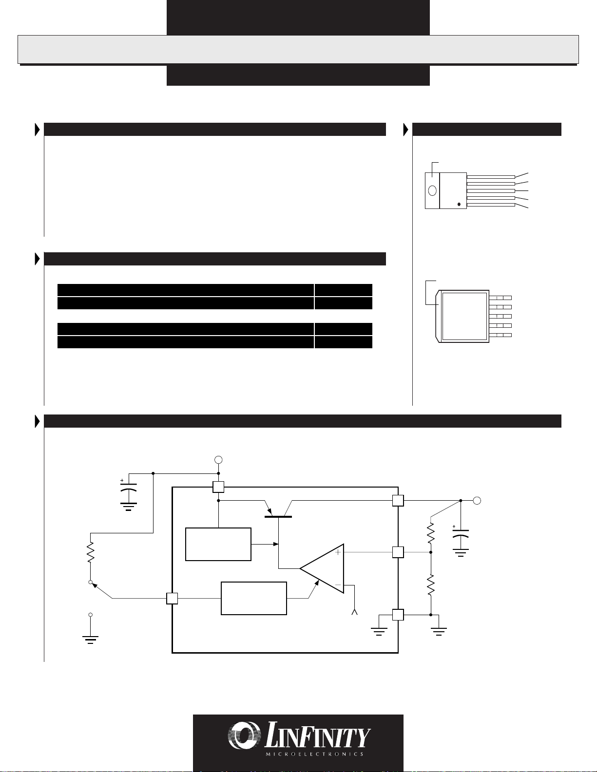
PACKAGE PIN OUTS
TAB IS GND
5
1
P PACKAGE
(Top View)
TAB IS GND
5
4
3
2
1
DD PACKAGE
(Top View)
ON/OFF
ADJ
GND
V
O
V
IN
ON/OFF
ADJ
GND
V
O
V
IN
C1*
0.1µF
ON
OFF
ON/
OFF
INPUT VOLTAGE
1
THERMAL
SHUTDOWN
5
BLOCK DIAGRAM
V
IN
ON/OFF
CIRCUIT
LX8941
* Required if regulator is located far from power supply
filter.
V
O
2
OUTPUT
VOLTAGE
C2
10µF
4
3
ADJ
GND
2
Copyright © 1999
Rev. 0.6 4/99
 Loading...