A
LIN DOC #:
LX8940
8940
5V L
T HE I NFINITE P OWER OF I NNOVATION
DESCRIPTION KEY FEATURES
The LX8940 is a 5V, low dropout, low
quiescent current regulator rated for 1A
of output current. It can regulate with
as low as 0.4V headroom between the
input and output voltages, thus
minimizing power dissipation. In
addition, it can be used in applications
where worst case supplies require a
NOTE: For current data & package dimensions, visit our web site: http://www.linfinity.com.
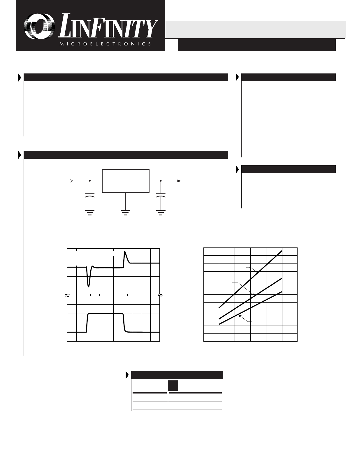
PRODUCT HIGHLIGHT
5.3V
IN
LX8940
low input-output differential to maintain
regulation. This feature makes it ideal
for computer monitors that have to
comply with energy-efficient / "Green
PC" programs, where the input voltage
drops to only a few tenths of a volt
above the output when power supply
enters sleep-mode operation.
OUT
GND
5V/100m
10µF0.1µF
OW DROPOUT REGULATOR
P RODUCTION DATA SHEET
■■
■ 2% Internally Trimmed Output
■■
■■
■ Output Current In Excess Of 1A
■■
■■
■ Input-Output Differential
■■
Less Than 0.4V At 1A
p Reverse Battery Protection
p 60V Load Dump Protection
p -50V Reverse Transient Protection
p Short Circuit Protection
p Internal Thermal Overload Protection
p Available In 3-Lead Plastic TO-220
p Drops In Most lM2940 Sockets
APPLICATIONS
■ Small Headroom Battery Applications
■ High Efficiency Linear Regulators
■ Post Regulators For Switching Power
Supplies
■ Green PC Monitor Applications
L OAD TRANSIENT RESPONSE
TA = 25°C
C
= 1µF
IN
= 5.30V
V
IN
5.000V
(20mV / Div.)
Output Voltage
4.980V
100mA
(50mA / Div.)
0mA
Output Current
CO = 47µF Electrolytic
Time - (20µs/Div.)
DROPOUT VOLTAGE VS. OUTPUT CURRENT
600
500
400
300
200
Dropout Voltage - (mV)
100
0
PACKAGE ORDER INFO
TA (°C)
0 to 125 LX8940CP
-40 to 125 LX8940IP
Plastic TO-220
P
3-pin
VS
. TEMPERATURE
125°C
25°C
100
Output Current - (mA)
500
-40°C
1000
Copyright © 1999
Rev. 1.3 3/99
L INF INITY MICROELECTRONICS INC.
11861 WESTERN AVENUE, GARDEN GROVE, CA. 92841, 714-898-8121, FAX: 714-893-2570
1

LX8940
PRODUCT DATABOOK 1996/1997
5V L
OW DROPOUT REGULATOR
RODUCTION DATA SHEET
P
ABSOLUTE MAXIMUM RATINGS (Note 1)
Input Voltage (VIN) .......................................................................................... -15V to 26V
Operating Junction Temperature
Plastic (P Package) ................................................................................................ 150°C
Storage Temperature Range ...................................................................... -65°C to 150°C
Lead Temperature (Soldering, 10 seconds) ............................................................. 300°C
Note 1. Exceeding these ratings could cause damage to the device. All voltages are with respect
to Ground. Currents are positive into, negative out of the specified terminal. Pin
numbers refer to DIL packages only.
THERMAL DATA
P PACKAGE:
THERMAL RESISTANCE-JUNCTION TO TAB,
THERMAL RESISTANCE-JUNCTION TO AMBIENT,
Junction Temperature Calculation: TJ = TA + (P
The θ
numbers are guidelines for the thermal performance of the device/pc-board system.
JA
All of the above assume no ambient airflow.
θθ
θ
θθ
JT
θθ
θ
θθ
JA
x θ
).
D
JA
3.0°C/W
60°C/W
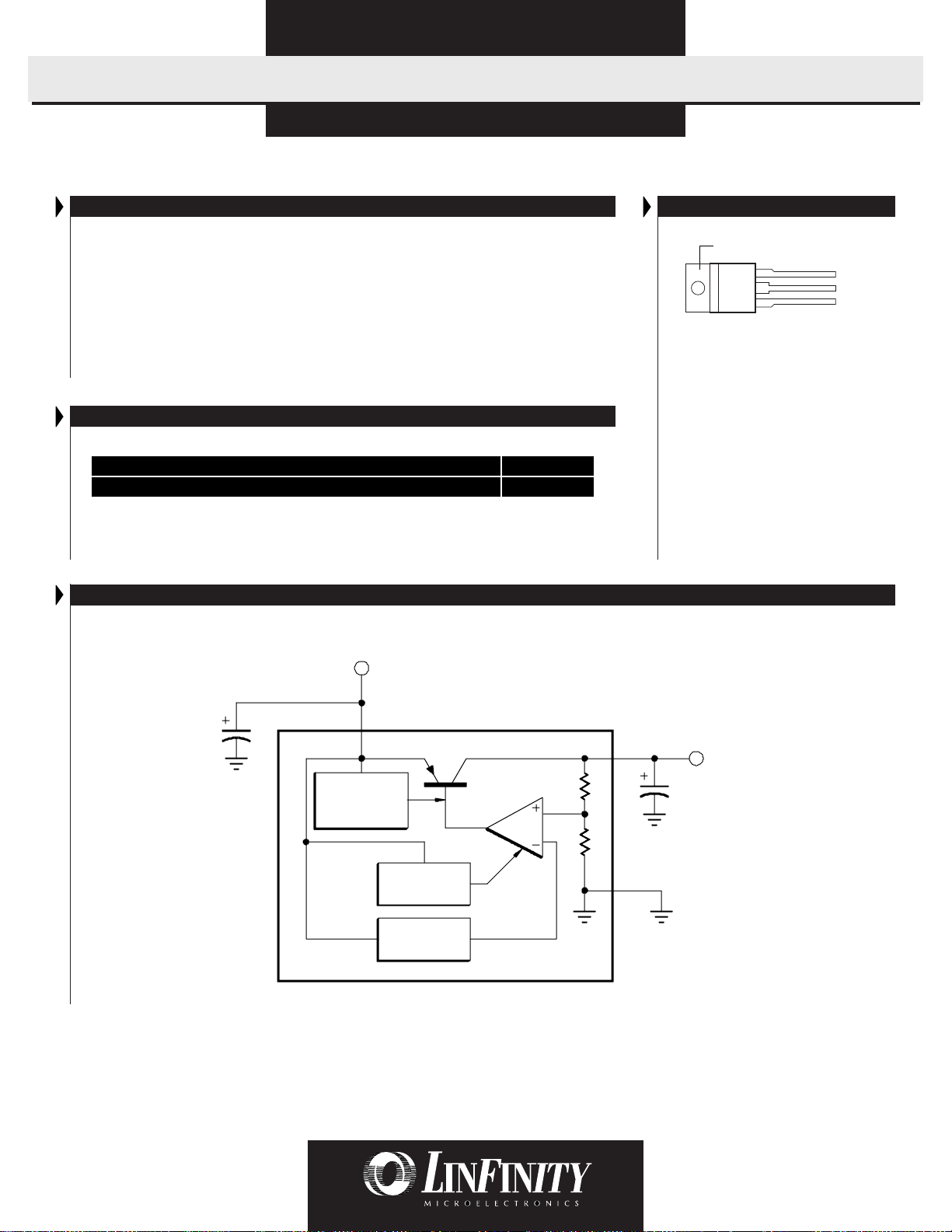
PACKAGE PIN OUTS
Tab is GROUND
3
2
1
P PACKAGE
(Top View)
OUTPUT
GND
INPUT
C1*
0.1µF
INPUT VOLTAGE
1 (INPUT)
OVERVOLTAGE
THERMAL
SHUTDOWN
REGULATOR
REFERENCE
BLOCK DIAGRAM
LX8940
BIAS
1.23V
* Required if regulator is located far from power supply filter.
3 (OUTPUT)
OUTPUT VOLTAGE
C2
10µF
2 (GND)
2
Copyright © 1999
Rev. 1.3 3/99
 Loading...