Microsemi Corporation LX8415-00CST, LX8415-33CST, LX8415-25CST Datasheet

LIN DOC #:
V
8415
LX8415-xx
0.5A LOW DROPOUT POSITIVE REGULATORS
T HE I NFINITE P OWER OF I NNOVATION
DESCRIPTION KEY FEATURES
The LX8415 series ICs are positive Low
Dropout (LDO) regulators. At the designed maximum load current, the
LX8415 series dropout voltage is guaranteed to be 1.3V or lower at 0.5A. The
dropout voltage decreases with load
current.
The LX8415 is available in an adjustable output voltage version and fixed
output versions of 2.5V and 3.3V. Onchip trimming of the internal voltage
reference allows specification of the
initial output voltage to within ±1% of
its nominal value. The output currentlimit point is also trimmed, which helps
NOTE: For current data & package dimensions, visit our web site: http://www.linfinity.com.
PRODUCT HIGHLIGHT
to minimize stress on both the regulator
and the system power source when they
are operated under short-circuit conditions. The regulator's internal circuitry
will operate at input-to-output differential voltages down to 1V.
Most regulator circuit designs include
output capacitors with values in the
range of tens to hundreds of microfarads
or more. The LX8415 typically requires
at least 10µF of output capacitance for
stable operation.
The LX8415 is available in the lowprofile plastic SOT-223 package for applications where space is at a premium.
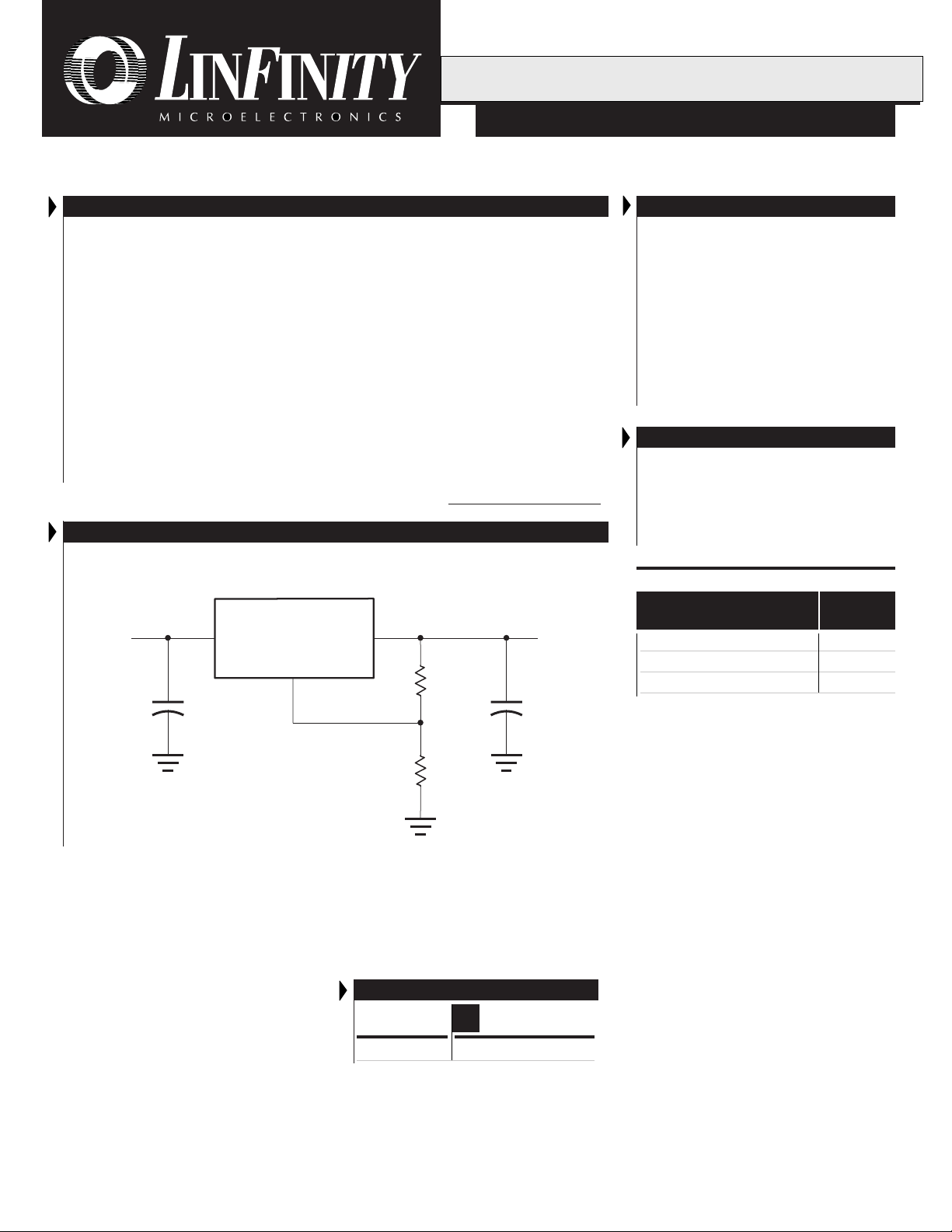
LOW COST 5V TO 3.3V REGULATOR
LX8415-xx
5V
IN
IN
ADJ
OUT
R
1
60.4
Ω
10µF 22µF
P RELIMINARY DATA SHEET
■ 0.7% Line Regulation Maximum
■ 0.7% Load Regulation Maximum
■ Output Current Of 500mA
■ Regulates To <1.3V Dropout
■ Space Saving SOT-223 Surface
Mount Package
■ Guaranteed Dropout Voltage At Multiple
Current Levels
■ 3-Terminal Adjustable, Fixed 2.5V And
Fixed 3.3V
APPLICATIONS
■ Battery Chargers
■ 5V To 3.3V Linear Regulators
■ Post Regulators For Switching Supplies
■ Modems
■ DVD Players
AVAILABLE OPTIONS PER PART #
V
OUT
3.3V
Part #
LX8415-25 2.5V
LX8415-33 3.3V
LX8415-00 Adjustable
Voltage
Output
R
2
100
Ω
PACKAGE ORDER INFO
(°C)
T
Note: All surface-mount packages are available in Tape & Reel.
Append the letter "T" to part number (i.e. LX8415-33CSTT).
"xx" refers to output voltage, please see table above.
Copyright © 1999
Rev. 0.4 1/99
11861 WESTERN AVENUE, GARDEN GROVE, CA. 92841, 714-898-8121, FAX: 714-893-2570
L INF INITY MICROELECTRONICS INC.
A
0 to 125 LX8415-xxCST
Plastic SOT-223
ST
3-pin
1

LX8415-xx
T
A
PRODUCT DATABOOK 1996/1997
0.5A LOW DROPOUT POSITIVE REGULATORS
RELIMINARY DATA SHEET
P
ABSOLUTE MAXIMUM RATINGS (Note 1)
Power Dissipation .................................................................................. Internally Limited
Input Voltage
LX8415-00 (Adjustable) / 8415-33 (3.3V) .................................................................. 7V
Surge Voltage ................................................................................................................. 7V
Operating Junction Temperature
Plastic (ST, DD & DT Packages) .......................................................................... 150°C
Storage Temperature Range ...................................................................... -65°C to 150°C
Lead Temperature (Soldering, 10 seconds) ............................................................. 300°C
Short-Circuit Protection ....................................................................................... Indefinite
Note 1. Exceeding these ratings could cause damage to the device. All voltages are with
respect to Ground. Currents are positive into, negative out of the specified terminal.
THERMAL DATA
ST PACKAGE:
THERMAL RESISTANCE-JUNCTION TO TAB,
THERMAL RESISTANCE-JUNCTION TO AMBIENT,
Junction Temperature Calculation: TJ = TA + (P
thermal performance of the device/pc-board system. All of the above assume no ambient airflow.
* θ
can be improved with package soldered to 0.5IN2 copper area over backside ground
JA
plane or internal power plane. θ
mounting technique. (See Application Notes Section: Thermal Considerations)
can vary from 20ºC/W to > 40ºC/W depending on
JA
θθ
θ
θθ
JT
θθ
θ
θθ
JA
x θJA). The θ
D
15°C/W
*150°C/W
numbers are guidelines for the
JA
PACKAGE PIN OUTS
TAB IS V
OUT
3. IN
2. OUT
1. ADJ / GND
ST PACKAGE
(Top View)
V
DJ
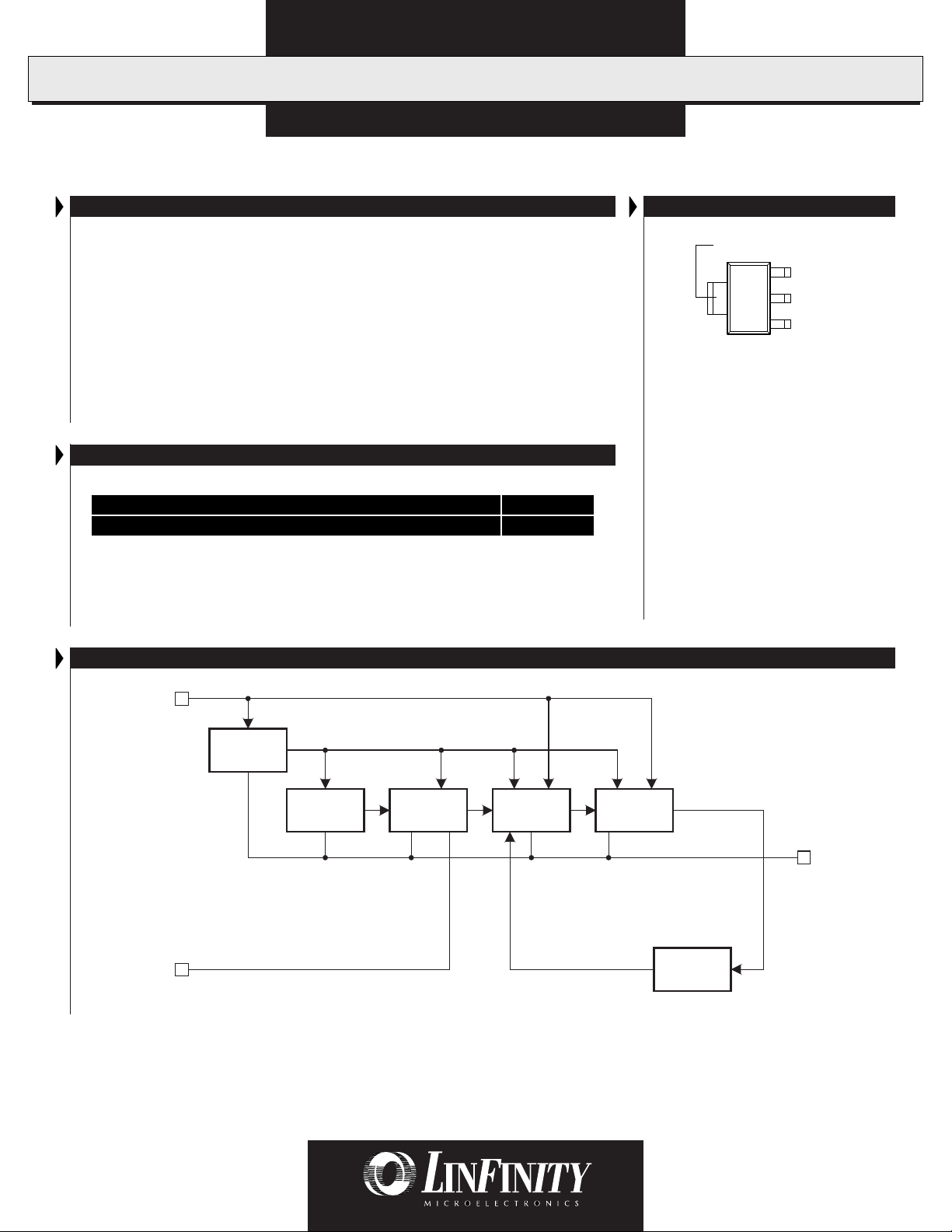
BLOCK DIAGRAM
IN
Bias
Circuit
Thermal
Limit Circuit
Bandgap
Circuit
Control
Circuit
Output
Circuit
Current
Limit Circuit
V
OU
2
Copyright © 1999
Rev. 0.4 1/99

PRODUCT DATABOOK 1996/1997
LX8415-xx
0.5A LOW DROPOUT POSITIVE REGULATORS
P RELIMINARY DATA SHEET
RECOMMENDED OPERATING CONDITIONS (Note 2)
Parameter
Symbol
Input Voltage
Operating Voltage LX8415-xx
Operating Ambient Temperature Range
Note 2. Range over which the device is functional.
ELECTRICAL CHARACTERISTICS
(Unless otherwise specified: 0°C ≤ TJ ≤ 125°C, I
Parameter
Reference Voltage LX8415-00 V
Output Voltage LX8415-25 I
LX8415-33 I
Line Regulation LX8415-00 I
(Note 3) LX8415-25 / 33 I
Load Regulation LX8415-00 (VIN - V
(Note 3) LX8415-25 / 33 V
Dropout Voltage LX8415-xx I
(Note 4) I
Current Limit LX8415-xx I
Minimum Load Current (Note 5) V
Quiescent Current LX8415-25 / 33 V
Thermal Regulation TA = 25°C, 30ms Pulse
Ripple Rejection f
Adjust Pin Current LX8415(A)-00
Adjust Pin Current Change
Temperature Stability
Long Term Stability TA = 125°C, 1000Hrs
RMS Output Noise (% of V
Notes: 3. See thermal regulation specification for changes in output voltage due to heating effects. Load regulation and line regulation are measured at a constant junction
temperature by low duty cycle pulse testing.
4. Dropout voltage is specified over the full output current range of the device. Dropout voltage is defined as the minimum input/output differential measured at the
specified output current. Test points and limits are also shown on the Dropout Voltage Curve.
5. Minimum load current is defined as the minimum output current required to maintain regulation.
LX8415(A)-00 10mA ≤ I
= 0.5A for the LX8415-xx.)
MAX
Symbol
REFIOUT
OUT (MAX)(VIN
= 10mA, (VIN - V
10mA ≤ I
= 10mA, VIN = 5V, TJ = 25°C
OUT
0mA ≤ I
= 10mA, VIN = 5V, TJ = 25°C
OUT
0mA ≤ I
= 10mA, 1.5V ≤ V
OUT
= 0mA, 4.75V ≤ VIN ≤ 6V
OUT
OUT
= 4.75V, 0mA ≤ I
IN
= 100mA
OUT
= 300mA
OUT
I
= I
OUT
MAX
- V
OUT
≤ 6V, (LX8415-00)
IN
≤ 6V
IN
= 120Hz, (VIN - V
RIPPLE
Test Conditions Units
) = 2V, TJ = 25°C
OUT
≤ I
, 1.5V ≤ (V
OUT
MAX
≤ I
, 4.75V ≤ VIN ≤ 6V
OUT
MAX
≤ I
, 4.75V ≤ VIN ≤ 6V
OUT
MAX
) = 3V, 10mA ≤ I
) ≥ 1.3V, T
≤ I
OUT
), 10Hz ≤ f ≤ 10kHz
OUT
OUT
= 25°C
J
, 1.5V ≤ (V
MAX
- V
IN
≤ I
OUT
- V
IN
≤ 6V
OUT
≤ I
OUT
MAX
) = 3V, V
- V
IN
MAX
Recommended Operating Conditions
Min. Typ. Max.
0 125 °C
Min. Typ. Max.
1.238 1.250 1.262 V
OUT
RIPPLE
OUT
) ≤ 6V
) ≤ 6V
= 1Vp - p
1.225 1.250 1.275 V
2.475 2.500 2.525 V
2.450 2.500 2.550 V
3.267 3.300 3.333 V
3.235 3.300 3.365 V
500 950 mA
Units
7V
LX8415-xx
0.05 0.7 %
17mV
0.15 0.5 %
10 20 mV
1.05 1.20 V
1.10 1.25 V
1.15 1.30 V
0.5 10 mA
4.5 10 mA
0.08 0.2 %/W
60 75 dB
60 130 µA
0.2 5 µA
0.5 %
0.3 %
0.003 %
Copyright © 1999
Rev. 0.4 1/99
3
 Loading...