Microsemi Corporation LX8385B-33CP, LX8385B-05CDD, LX8385B-00CP, LX8385B-00CDD, LX8385A-33CP Datasheet
...
DESCRIPTION KEY FEATURES
■■
■■
■ Three-Terminal Adjustable Or Fixed
Output Voltage
■■
■■
■ Guaranteed 1% Voltage Reference
Accuracy Over Line, Load And
Temperature (LX8385B)
■■
■■
■ Guaranteed < 1.5V Headroom At 3A
(LX8385)
■■
■■
■ Guaranteed < 1.3V Headroom At 3A
(LX8385A/8385B)
■■
■■
■ Output Current Of 3A Minimum
p 0.015% Line Regulation
p 0.1% Load Regulation
The LX8385/8385A/8385B series ICs are
positive regulators designed to provide
3A output current. Each regulator yields
higher efficiency than currently available
devices with all internal circuitry designed
to operate down to a 1V input-to-outputdifferential. In these products, the dropout voltage is fully specified as a function
of load current. The LX8385's dropout is
guaranteed at a maximum of 1.5V at maximum output current, decreasing at lower
load currents. The LX8385A/85B have a
maximum dropout voltage of 1.3V.
The LX8385B offers a tighter voltage
reference tolerance: ±1.0% over line, load
and temperature, with 0.8% initial accuracy. The LX8385/85A have 1.0% initial
accuracy, with 2% over line, load and temperature.
The LX8385/85A/85B series devices are
pin-compatible with earlier 3-terminal
regulators, such as 117 series products.
While a 10µF output capacitor is required
on both input and output of these new
devices, this is generally included in most
regulator designs.
The quiescent current of the LX8385/
85A/85B series products flows into the
load, increasing efficiency. This feature
contrasts with PNP regulator designs,
where up to 10% of the output current is
wasted as quiescent current.
The LX8385-xxI is rated for -25°C to
+125°C applications, and the LX8385-xxC
/8385B-xxC is rated for 0°C to +125°C
applications.
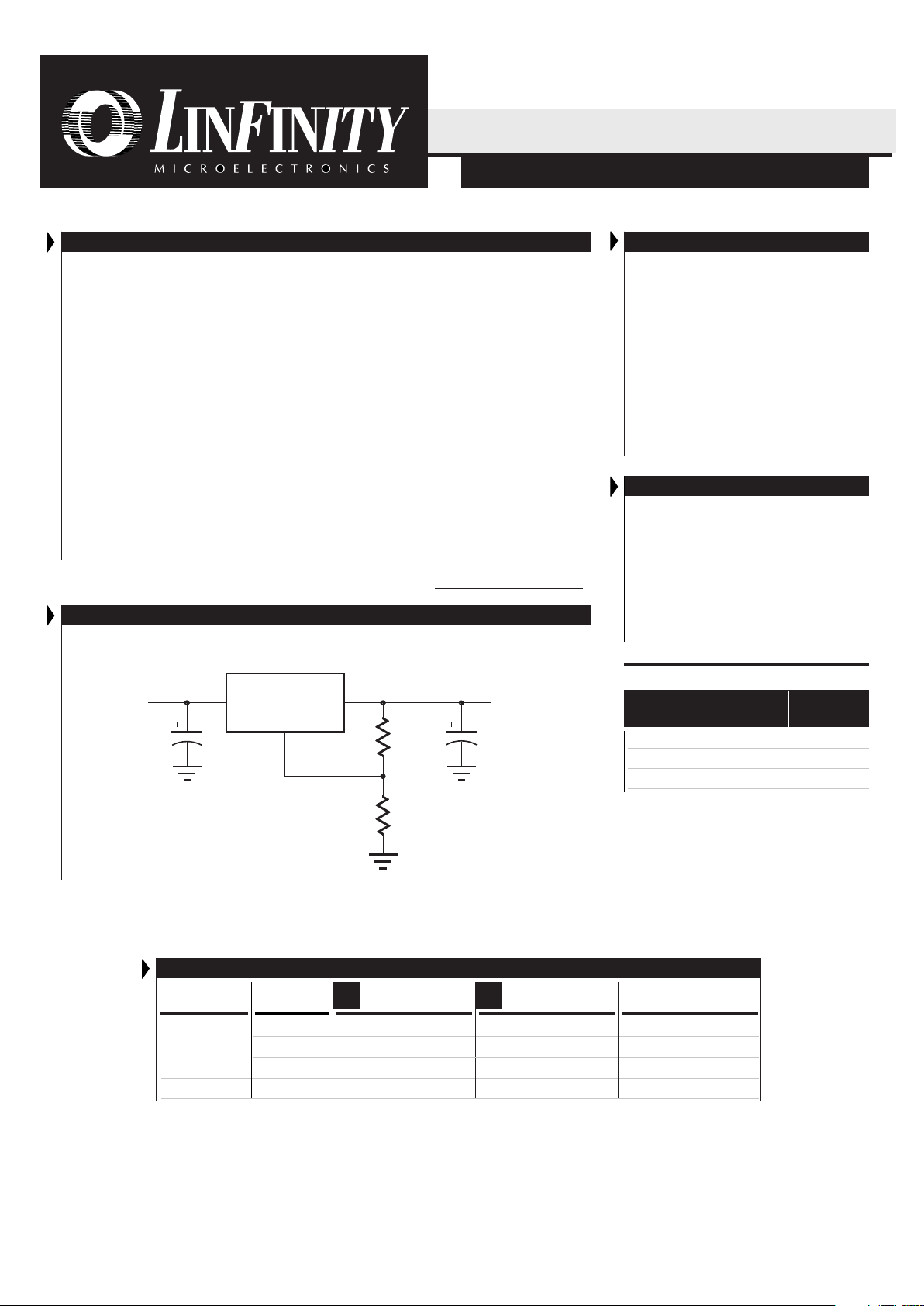
PRODUCT HIGHLIGHT
3.3V, 3 A REGULATOR
APPLICATIONS
■ High Efficiency Linear Regulators
■ Post Regulators For Switching
Power Supplies
■ Battery Chargers
■ Constant Current Regulators
■ Graphics & Standard Supplies
■ Processor I/O Supply
■ Low Voltage Memory & Chipset Supplies
3A LOW D
ROPOUT POSITIVE REGULATORS
P RODUCTION DATA SHEET
T HE I NFINITE P OWER OF I NNOVATION
LX8385-xx/8385A-xx/8385B-xx
LIN DOC #:
8385
LX8385
200
Ω
1%
1%
3.3V at 3A
5V
OUT
IN
ADJ
1500µF, 6.3V
6MV1500GX
2x 1500µF, 6.3V
6MV1500GX
from Sanyo
121Ω
Note: All surface-mount packages are available in Tape & Reel. Append the letter "T" to part number
(i.e. LX8385-00CDDT). "xx" refers to output voltage, please see table above.
* Consult factory for availability of TO-3 Metal Can.
LX8385/85A/85B-00 Adjustable
LX8385/85A/85B-33 3.3V
LX8385/85A/85B-05 5.0V
Part #
Output
Voltage
AVAILABLE OPTIONS PER PART #
Other voltage options may be available —
Please contact factory for details.
PACKAGE ORDER INFORMATION*
T
A
(°C)
P
1.5VLX8385-xxCPLX8385-xxCD
0 to 1251.3VLX8385A-xxCPLX8385A-xxCD
1.3VLX8385B-xxCPLX8385B-xxCD
-25 to 1251.5VLX8385-xxIPLX8385-xxID
Dropout
Voltage
Plastic TO-220
3-pin
Plastic TO-263
3-pin
DD
Copyright © 1999
Rev. 2.0a 10/00
1
11861 WESTERN AVENUE, GARDEN GROVE, CA. 92841, 714-898-8121, FAX: 714-893-2570
L INF INITY MICROELECTRONICS INC.
NOTE: For current data & package dimensions, visit our web site: http://www.linfinity.com.

3A LOW D
ROPOUT POSITIVE REGULATORS
LX8385-xx/8385A-xx/8385B-xx
PRODUCT DATABOOK 1996/1997
Copyright © 1999
Rev. 2.0a 10/00
2
P
RODUCTION DATA SHEET
ABSOLUTE MAXIMUM RATINGS (Note 1)
Power Dissipation .................................................................................. Internally Limited
Input Voltage................................................................................................................ 10V
Input to Output Voltage Differential ........................................................................... 10V
Operating Junction Temperature
Plastic (P, DD & DL Packages)............................................................................. 150°C
Storage Temperature Range ...................................................................... -65°C to 150°C
Lead Temperature (Soldering, 10 seconds) ............................................................. 300°C
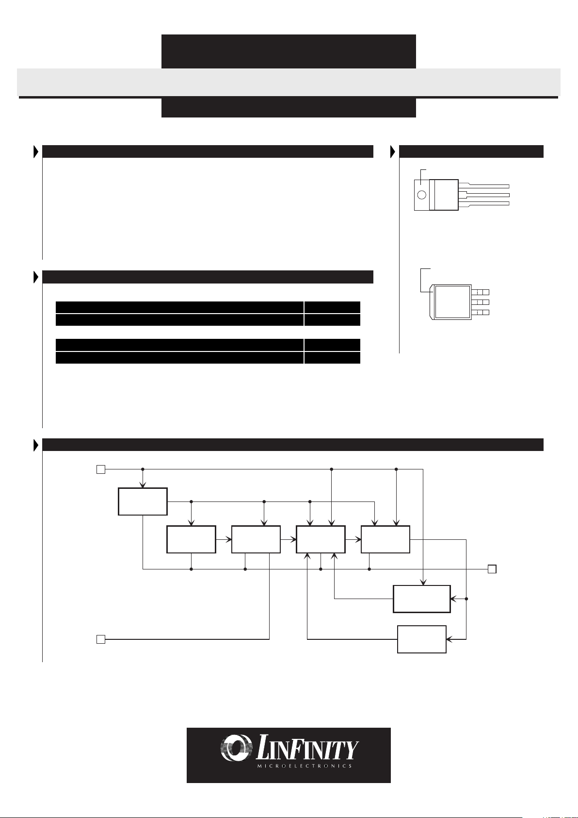
PACKAGE PIN OUTS
Thermal
Limit Circuit
Control
Circuit
Bandgap
Circuit
Output
Circuit
Bias
Circuit
V
OUT
V
IN
SOA Protection
Circuit
Current
Limit Circuit
ADJ or
GND*
BLOCK DIAGRAM
P PACKAGE:
THERMAL RESISTANCE-JUNCTION TO TAB,
θθ
θθ
θ
JT
3.0°C/W
THERMAL RESISTANCE-JUNCTION TO AMBIENT,
θθ
θθ
θ
JA
60°C/W
DD PACKAGE:
THERMAL RESISTANCE-JUNCTION TO TAB,
θθ
θθ
θ
JT
3.0°C/W
THERMAL RESISTANCE-JUNCTION TO AMBIENT,
θθ
θθ
θ
JA
*60°C/W
Junction Temperature Calculation: TJ = TA + (P
D
x θ
JA
).
The θ
JA
numbers are guidelines for the thermal performance of the device/pc-board system.
All of the above assume no ambient airflow.
* θ
JA
can be improved with package soldered to 0.5IN2 copper area over backside ground
plane or internal power plane. θ
JA
can vary from 20ºC/W to > 40ºC/W depending on
mounting technique.
THERMAL DATA
3
2
1
P PACKAGE
(Top View)
* Pin 1 is GND for fixed voltage versions.
3
2
1
DD PACKAGE
(Top View)
* Pin 1 is GND for fixed voltage versions.
Note 1. Exceeding these ratings could cause damage to the device. All voltages are with
respect to Ground. Currents are positive into, negative out of the specified terminal.
TAB IS V
OUT
TAB IS V
OUT
* This pin GND for fixed voltage versions.
V
IN
V
OUT
ADJ / GND*
V
IN
V
OUT
ADJ / GND*

3A LOW D
ROPOUT POSITIVE REGULATORS
LX8385-xx/8385A-xx/8385B-xx
PRODUCT DATABOOK 1996/1997
3
Copyright © 1999
Rev. 2.0a 10/00
P RODUCTION DATA SHEET
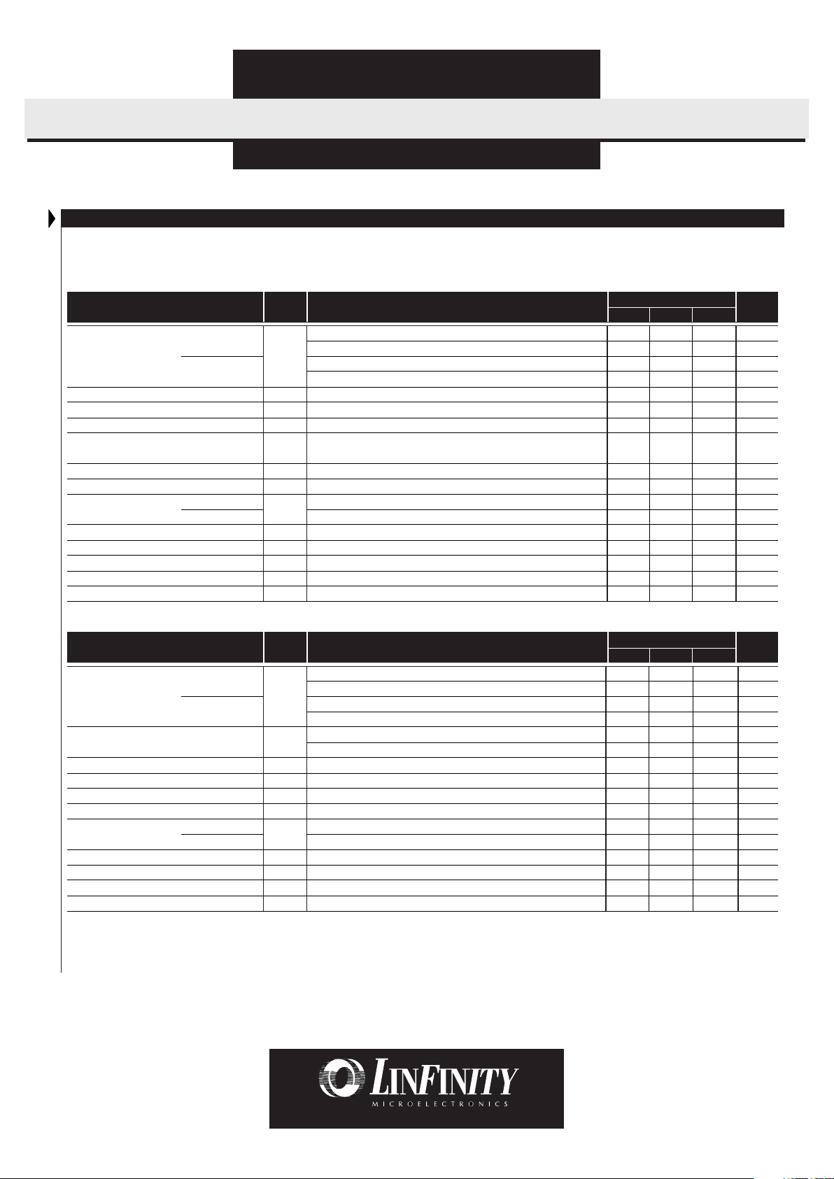
ELECTRICAL CHARACTERISTICS
(Unless otherwise specified, these specifications apply over the operating ambient temperatures for the LX8385-xxC/85A/85B-xxC with 0°C ≤ TA ≤
125°C and the LX8385-xxI with -25°C ≤ TA ≤ 125°C; V
IN
- V
OUT
= 3V; I
OUT
= 3A. Low duty cycle pulse testing techniques are used which maintains
junction and case temperatures equal to the ambient temperature.)
Parameter
Symbol
Test Conditions Units
LX8385/85A/85B-00
Min. Typ. Max.
Reference Voltage LX8385-00 V
REFIOUT
= 10mA, TA = 25°C
(Note 4) 10mA ≤ I
OUT
≤ I
OUT (MAX)
, 1.5V ≤ (V
IN
- V
OUT
), V
IN
≤ 10V, P ≤ P
MAX
LX8385A/85B-00
I
OUT
= 10mA, TA = 25°C
10mA ≤ I
OUT
≤ I
OUT (MAX)
, 1.5V ≤ (V
IN
- V
OUT
), V
IN
≤ 10V, P ≤ P
MAX
Line Regulation (Note 2)
∆V
REF
(VIN)
1.5V ≤ (V
IN
- V
OUT
) ≤ 7V, I
OUT
= 10mA
Load Regulation (Note 2)
∆V
REF
(I
OUT
)
VIN - V
OUT
= 3V, 10mA ≤ I
OUT
≤ 3A
Thermal Regulation
∆V
OUT
(Pwr)
TA = 25°C, 20ms pulse
Ripple Rejection (Note 3) V
OUT
= 5V, f =120Hz, C
OUT
= 100µf Tantalum, VIN = 6.5V
C
ADJ
= 10µF, I
OUT
= 3A
Adjust Pin Current I
ADJ
Adjust Pin Current Change (Note 4) ∆ I
ADJ
10mA ≤ I
OUT
≤ I
OUT (MAX)
, 1.5V ≤ (V
IN
- V
OUT
), V
IN
≤ 10V
Dropout Voltage LX8385-00 ∆ V ∆V
REF
= 1%, I
OUT
= 3A
LX8385A/85B-00
∆V
REF
= 1%, I
OUT
= 3A
Minimum Load Current I
OUT (MIN)VIN
≤ 10V
Maximum Output Current I
OUT (MAX)(VIN
- V
OUT
) ≤ 7V, VIN ≤ 10V
Temperature Stability (Note 3) ∆V
OUT
(T)
Long Term Stability (Note 3) ∆V
OUT
(t) TA = 125°C, 1000 hours
RMS Output Noise (% of V
OUT
) (Note 3) V
OUT (RMS)TA
= 25°C, 10Hz ≤ f ≤ 10kHz
1.238 1.250 1.262 V
1.225 1.250 1.270 V
1.240 1.250 1.260 V
1.238 1.250 1.262 V
0.015 0.2 %
0.2 0.5 %
0.01 0.04 %/W
65 83 dB
55 100 µA
0.2 5 µA
1.2 1.5 V
1.1 1.3 V
210mA
3 3.5 A
0.25 %
0.3 1 %
0.003 %
Parameter
Symbol
Test Conditions Units
LX8385/85A/85B-33
Min. Typ. Max.
Output Voltage LX8385-33 V
OUTVIN
= 5V, I
OUT
= 0mA, TA = 25°C
(Note 4) 4.75V ≤ VIN ≤ 10V, 0mA ≤ I
OUT
≤ 3A, P ≤ P
MAX
LX8385A/85B-33
VIN = 5V, I
OUT
= 0mA, TA = 25°C
4.75V ≤ VIN ≤ 10V, 0mA ≤ I
OUT
≤ 3A, P ≤ P
MAX
Line Regulation (Note 2) ∆V
OUT
4.75V ≤ VIN ≤ 7V
(VIN)
4.75V ≤ VIN ≤ 10V
Load Regulation (Note 2)
∆V
OUT(IOUT
)
V
IN
= 5V, 0mA ≤ I
OUT
≤ I
OUT (MAX)
Thermal Regulation
∆V
OUT
(Pwr)
TA = 25°C, 20ms pulse
Ripple Rejection (Note 3) C
OUT
= 100µF (Tantalum), I
OUT
= 3A
Quiescent Current I
Q
0mA ≤ I
OUT
≤ I
OUT (MAX)
, 4.75V ≤ VIN ≤ 10V
Dropout Voltage LX8385-33 ∆V ∆V
OUT
= 1%, I
OUT
≤ I
OUT (MAX)
LX8385A/85B-33
∆V
OUT
= 1%, I
OUT
≤ I
OUT (MAX)
Maximum Output Current I
OUT (MAX)VIN
≤ 7V
Temperature Stability (Note 3) ∆V
OUT
(T)
Long Term Stability (Note 3) ∆V
OUT
(t) TA = 125°C, 1000 hours
RMS Output Noise (% of V
OUT
) (Note 3) V
OUT (RMS)TA
= 25°C, 10Hz ≤ f ≤ 10kHz
3.267 3.3 3.333 V
3.235 3.3 3.365 V
3.274 3.3 3.326 V
3.267 3.3 3.333 V
16mV
210mV
515mV
0.01 0.02 % / W
60 83 dB
410mA
1.2 1.5 V
1.1 1.3 V
3 3.5 A
0.25 %
0.3 1 %
0.003 %
Note 2. Regulation is measured at constant junction temperature, using pulse testing with a low duty cycle. Changes in output voltage due to
heating effects are covered under the specification for thermal regulation.
Note 3. These parameters, although guaranteed, are not tested in production.
Note 4. See Maximum Output Current Section above.
LX8385-00/85A/85B-00 (Adjustable)
LX8385-33/85A-33/85B-33 (3.3V Fixed)
 Loading...