

查询LX8221供应商
TM
The LX8221 family of dual output
linear regulators provide for the
selection of either fixed or adjustable
output voltages, and combine low
dropout operation, fast transient
performance, tight output voltage
accuracy, and ultra-low ground current
within a very small package footprint.
The PMOS output transistor allows
for an ultra-low dropout characteristic
(e.g., typically less than 175mV at
100mA). The individual regulators can
be powered from either separate supply
voltages or the same supply voltage
between 2.8V to 6V allowing for
maximum system flexibility.
An optional ceramic or tantalum type
capacitor may be connected to each
Bypass pin separately to improve
performance in critical low-noise
applications.
IMPORTANT: For the most current data, consult MICRO Semi’s website: http://www.microsemi.com
5.0V
3.3V
VIN2
VIN1
CB1
DESCRIPTION
Overall regulator efficiency has been
improved with a minimized operating
ground current (typ < 140µA per
regulator). Further, this ground current
is virtually eliminated in shutdown mode
(typ < 1µA).
Other safety features include channel
independent Thermal and Short Circuit
Current protection.
Separate Enable pins allow each
regulator to be switched on and off
independently by applying a TTL logic
level control signal to the Enable pin
further enhancing system level power
management.
These features combined with a small
footprint (i.e., 10-pin MSOP package)
make the LX8221 especially useful for
battery-operated equipment such as
cellular telephones, laptop computers
and PDA equipment.
PRODUCT HIGHLIGHT
N/C
EN1
EN2
VOUT1
To Control Logic
}
Off
LX8221
®
Dual 150mA CMOS Low Dropout Regulator
KEY FEATURES
Compact regulators with
two 150 mA outputs
Dropout Voltage typically
175mV @ 100mA
Ultra low shutdown Current
typically less than 1µA
Output trimmed to 0.5%
Small MSOP-10 package
Over Current &
Temperature protection
Stable with ceramic or
tantalum capacitors
WWW.Microsemi .COM
APPLICATIONS
Battery Operated Systems
Laptop, Notebook and PDA’s
Cellular Telephones/pagers
Instrumentation
Linear post regulators for
N/C
SMPS
EN1
EN2
VOUT1
To Control Logic
}
Off
On
5.0V
On
3.3V
VIN2
VIN1
ADJ1
Copyright © 2000
Rev. 1.0a, 2005-03-03
ADJ
Fixed / Adjustable Application
TJ (°C)
VOUT2
GND
R1
R2
PACKAGE ORDER INFO
VOUT1 VOUT2
-40 to 125 Adjustable Adjustable
-40 to 125 2.5V Adjustable
-40 to 125 2.7V Adjustable
-40 to 125 3.0V Adjustable
Note: Available in Tape & Reel. Append the letter “T” to the part number. (i.e. LX8221AIDU-TR)
Contact Microsemi for additional / available options
Microsemi
11861 Western Avenue, Garden Grove, CA. 92841, 714-898-8121, Fax: 714-893-2570
Linfinity Microelectronics Division
VOUT2
GND
Package Marking
8221 AIDU LX
8221 BIDU LX
8221 DIDU LX
8221 GIDU LX
R1
R2
L
L
X
X
8
8
2
2
2
2
1
1
ADJ2
R1R2
Plastic MSOP 10-Pin
DU
RoHS Compliant / Pb-free
Transition D/C: 0432
Adjustable / Adjustable Application
LX8221AIDU
LX8221BIDU
LX8221DIDU
LX8221GIDU
Page 1
TM
Input Voltage (VIN1, VIN2).......................................................................... -0.3V to +7V
Output Current (I
Operating Temperature Range .....................................................................-40 to +125 °C
Maximum Junction Temperature (T
Storage Temperature (T
Peak Package Solder Reflow Temp. (40 second max. exposure)................. 260°C (+0, -5)
Note: Exceeding these ratings could cause damage to the device. All voltages are with respect to
Ground. Currents are positive into, negative out of specified terminal.
ABSOLUTE MAXIMUM RATINGS
, I
OUT1
)................................................................................. 150mA
OUT2
) ......................................................................150 °C
) .............................................................................-65 to +150 °C
J
J
®
Dual 150mA CMOS Low Dropout Regulator
VOUT1
VOUT1/VOUT2 Regulated output voltage. Regulator stability is achieved with external capacitor of 1uF
Plastic MSOP 8-Pin
DU
THERMAL RESISTANCE-JUNCTION TO AMBIENT,
THERMAL RESISTANCE-JUNCTION TO CASE,
Junction Temperature Calculation: TJ = TA + (PD x θ
numbers are guidelines for the thermal performance of the device/pc-board
The θ
JA
system. All of the above assume no ambient airflow.
P
IN NAME
VIN1/VIN2 Unregulated input supply voltage
GND Ground Pin
EN1/EN2 Enable control input: Logic high = Enable; logic low or open = Shutdown
ADJ (1, 2) Adjust pin. Connect a resistor divider to this pin to establish preferred output voltage.
D
CB1 Reference bypass input. Adding an additional external capacitor reduces output noise.
THERMAL DATA
θ
JC
).
JC
FUNCTIONAL PIN DESCRIPTION
θ
JA
206°C/W
39°C/W
ESCRIPTION
LX8221
PACKAGE PIN OUT
1
CB1
NC
EN2
VIN2
RoHS / Pb-free 100% Matte Tin Lead Finish
2
3
4
56
DU
(Top View)
“NC” = No Internal Connection
FRONT MARKING
8221
xIDU
x = Voltage Combination
i.e. A = Adj/Adj
PACKAGE
LX
10
9
8
7
WWW.Microsemi .COM
VIN1
EN1
GND
ADJ
VOUT2
Copyright © 2000
Rev. 1.0a, 2005-03-03
Microsemi
Linfinity Microelectronics Division
11861 Western Avenue, Garden Grove, CA. 92841, 714-898-8121, Fax: 714-893-2570
Page 2
P
P
A
A
C
C
K
K
A
A
G
G
E
E
D
D
A
A
T
T
A
A
(
)
TM
VOUT1
THERMAL
CB1
GND
SENSOR
+
-
VREF
CONTROL
LOGIC
CURRENT
LIMIT
®
Dual 150mA CMOS Low Dropout Regulator
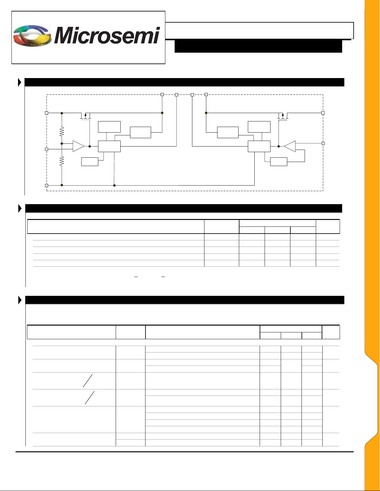
BLOCK DIAGRAM
VIN1
EN1
EN2
VIN2
CURRENT
LIMIT
THERMAL
SENSOR
CONTROL
LOGIC
Parameter Symbol
Input Operating Voltage Range (Note 1) VIN1, VIN2 2.5 6 V
Enable Input Voltage Range EN1/2 VIN + 0.3V V
Continuous Output Current Range I
Input Capacitor (VIN to GND) CIN 1.0* µF
Output Capacitor (V
Note 1: The minimum VIN has to meet two conditions V
* Size your output capacitor to meet the transient loading requirement. If you have a very dynamic load, a lower ESR and larger value capacitor will improve the response to
these load steps.
OUT
RECOMMENDED OPERATING CONDITIONS
OUT1, IOUT
to GND) C
> 2.5V and V
IN
> V
+ V
IN
OUT
DROPOUT
.
OUT
LX8221
Min Typ Max
150 mA
1
1.0* 2.2 µF
Unless otherwise specified, the following specifications apply over the operating ambient temperature -40°C≤ T
where otherwise noted. Test conditions: V
testing methods.
Parameter Symbol Test Conditions
Output Voltage (2.5, 2.7, 3.0, ADJ) VOUT1/2
Adjust Reference Voltage V
V
Line Regulation
Load Regulation
∆
⎛
O
⎜
⎝
V
∆
⎛
⎜
⎝
⎞
⎟
V
∆
IN
⎠
⎞
O
⎟
I
∆
O
⎠
Dropout Voltage
(Note 2)
VV −
OIN
Ground Pin Current
ELECTRICAL CHARACTERISTICS
= V
IN
+ 0.5V; I
OUT
TJ = 25°C -1 1
0mA
≤
TJ = 25°C 1.163 1.187
ADJ
0mA
I
≤
V
(V
RV
OUT1/2
TJ = 25°C, 0.5mA≤I
V
RI
0.5mA
I
LOAD1/2
I
= 50mA, ∆VO = -1%
LOAD1/2
V
DO
I
= 100mA, ∆VO = -1%
LOAD1/2
I
= 150mA, ∆VO = -1%
I
I
STBY
GND
LOAD1/2
EN1 = High, EN2 = High 280 440
EN1 = Low, EN2 = Low 1
=10mA; CIN = 1µF; C
OUT
I
150mA, (V
≤
OUT1/2
150mA, 2.85V≤V
≤
OUT1/2
+ 0.5V)≤V
I
≤
OUT1/2
100mA
≤
IN
6V, I
≤
OUT1/2
= 1mA, ∆VO = -1%
OUT1/2
OUT1/2
150mA
≤
OUT
+ 0.5V)≤V
6V
≤
IN
= 0.1mA
= 1µF; TJ = T
Min Typ Max
6V
≤
IN
-2.5 2.5
1.140
0.04 0.15 %/V
0.5
1.5
0.050
0.175
0.175 0.3
0.25 0.4
LX8221
VOUT2
+
-
VREF
≤
125°C except
using low duty cycle pulse
A
A
LX1742
1.175
1.210
ADJ
Units
Units
%V
µA
WWW.Microsemi .COM
%
V
NOM
V
Copyright © 2000
Rev. 1.0a, 2005-03-03
Microsemi
Linfinity Microelectronics Division
11861 Western Avenue, Garden Grove, CA. 92841, 714-898-8121, Fax: 714-893-2570
Page 3

TM
Adjust Input Bias Current I
Enable Pin Current IEN V
Enable Threshold
Short Circuit Current Limit I
Power Supply Rejection Ratio
Output Noise eN TJ = 25°C, C
Thermal Shutdown Temperature TSD 170 °C
Note 2: Dropout voltage is defined as the input to output differential at which the output voltage drops 1% below the nominal value. Dropout voltage specification
applies only to output voltages greater than 2.8 V. For output voltages below 2.8 V, the dropout voltage is nothing but the input to output differential, since the
minimum input voltage is 2.8 V.
V
ADJ
V
2.0
EN(IH)
V
0.4
EN(IL)
VOUT1 = 0V, VOUT2 = 0V 400 mA
OUT(SC)
PSRR
TJ = 25°C, f = 120Hz 50 dB
®
= 1.25V 100 nA
ADJ
= VIN 100 nA
EN1/2
Dual 150mA CMOS Low Dropout Regulator
= 10uF,C
OUT
= 470 pF 50 µV
BYPASS
Description
The LX8221 family of LDO linear regulators is available
in a 10-pin MSOP Package and provides a cost effective
power management solution for battery driven applications.
The regulator family includes both fixed/adjustable and
adjustable/adjustable output voltage versions. The internal
PMOS power device provides low dropout regulation with
a fast line and load transient response. It also includes
internal current limiting and thermal shutdown circuitry. In
this section you will find information about capacitor,
thermal, and layout design considerations.
Input Capacitor
To improve load transient response and noise rejection a
bypass capacitor is recommended (but it is not required for
stability). There are no requirements for the ESR
(Equivalent Series Resistor) on the input capacitor, but
tolerance and temperature coefficient must be considered
when selecting this capacitor to ensure that the capacitor’s
value will be around 1
µ
F over the entire operating
temperature range. For the LX8221, a 1
capacitor may be connected between both VIN1/2 and
ground.
Output Capacitor
The LX8221 uses an internal feedback loop to maintain a
constant output voltage. This feedback loop induces a
natural phase shift and the amount of phase shift
determines the loop’s stability. Therefore, like any lowdropout regulator, an output capacitor with low ESR
(Equivalent Series Resistance) is required between VOUT
and GND to stabilize the internal control loop. A ceramic,
APPLICATIONS
µ
F ceramic type
LDO’s stability. The LX8221-x adjustable regulator’s
output voltage can be externally set by connecting the ADJ
pin/s to an external resistor divider (See Figure 1 and 2).
The output voltage can be calculated using the formula:
OUT
⎟
⎜
R
2
⎠
⎝
⎞
⎛
R
1
⎟
⎜
+=
1VV
ADJ
Enable
The Enable pin allows the LX8221 to be independently
turned on and off. The Enable pins are compatible with
standard TTL-CMOS levels. A logic zero (0.4V) on the En
En
pins shuts the LX8221 off and reduces the supply
2
current to less than 1µA (typ). Pulling the Enable inputs high
(2.0V) causes normal operation to resume. If the Enable
feature is not used, this pin can be connected to V
Minimum Load Requirement
Although line regulation is improved with a minimum load
of 100µA, the LX8221 does not have a minimum load
current in order to maintain stability. This is an especially
important feature in certain applications.
Temperature Protection
The thermal protection shuts the LX8221 down when the
junction temperature exceeds approximately 150
no appreciable thermal hysteresis.
Short Circuit Current Protection
The LX8221 includes over-current protection, when the
output load current exceeds about 400mA. When this
occurs, the protection circuit forces the regulator to decrease
LX8221
V
1
.
IN
0
C; there is
WWW.Microsemi .COM
/
Copyright © 2000
Rev. 1.0a, 2005-03-03
Microsemi
Linfinity Microelectronics Division
11861 Western Avenue, Garden Grove, CA. 92841, 714-898-8121, Fax: 714-893-2570
Page 4

(
)
(
)
TM
tantalum or electrolytic capacitor with a minimum
recommended capacitance value of 1.0
µ
F and ESR
between 5mΩ and 1Ω will satisfy the stability for the entire
operating range.
Optional Bypass Capacitor
The fixed/adjustable voltage version of the LX8221
includes a separate Bypass pin (CB1) for the fixed
regulator that allows for further reduction of output noise.
If the regulator’s output noise performance meets system
design specifications without the capacitor, omit it. The
bypass capacitor impacts the start up time, which is
inversely proportional to the size of bypass capacitor.
Further, the bypass capacitor reduces the regulator phase
margin. Hence, implementing the bypass capacitor will
require the use of a larger output capacitor to maintain the
be calculated using the following equation:
IVVP ×−=
)()()( MAXOUTMINOUTMAXIND
(Note: power dissipation resulting from quiescent current
is negligible)
For the MSOP package, thermal resistance,
θ
is 2200C/W
JA
when mounted on a FR4 copper clad PCB. Junction
temperature of the integrated circuit can be calculated
using:
TTT +=
RISEAJ
Where:
()
PT Θ×=
JADRISE
Example: Given the following conditions:
T
= 60°C
A
V
= 4.2V
IN
V
= 2.7V
OUT
I
= 100mA
OUT
®
Dual 150mA CMOS Low Dropout Regulator
its output current.
Thermal Consideration
Thermal shutdown protects the integrated circuit from
thermal overload caused from a rise in junction temperature
during power dissipation. This type of protection is intended
for fault protection only and not as a means of current (or,
power) limiting during normal application usage. Proper
thermal evaluation should be done to ensure that the junction
temperature dose not exceed it’s maximum rating. Operating
at the maximum T
variation in individual device electrical characteristics and
thermal resistance, the built in thermal overload protection
may be activated at power levels slightly above or below the
rated dissipation. Power dissipation for each regulator can
APPLICATIONS
calculate the total power dissipation and junction
temperature:
Total Power Dissipation:
Junction Temperature:
Layout Consideration:
The layout must be implemented with low impedance paths
IN
, V
for V
traces to avoid voltage drops and pick up noise. Adding an
area of PCB copper to the GND pin (pin 8) will reduce the
overall
θ
JA
substrate. This will lower the device junction temperature
improving overall output voltage accuracy. The input/output
capacitors must be placed as close as possible to each
voltage regulator output pin.
LX8221
of 150°C can impact reliability. Due to
J
()
D
=×−=
J
and Ground by creating sufficiently wide
OUT
since it is thermally connected to the device
W15.0A1.0V7.2V2.4P
ooo
CWCWCT
93/22015.060 =×+=
WWW.Microsemi .COM
Copyright © 2000
Rev. 1.0a, 2005-03-03
Microsemi
Linfinity Microelectronics Division
11861 Western Avenue, Garden Grove, CA. 92841, 714-898-8121, Fax: 714-893-2570
Page 5

LX8221
TM
5.0V
3.3V
APPLICATION CIRCUITS
®
VIN2
VIN1
CB1
ADJ
Dual 150mA CMOS Low Dropout Regulator
Resistor Table
N/C
GND
EN1
EN2
VOUT1
VOUT2
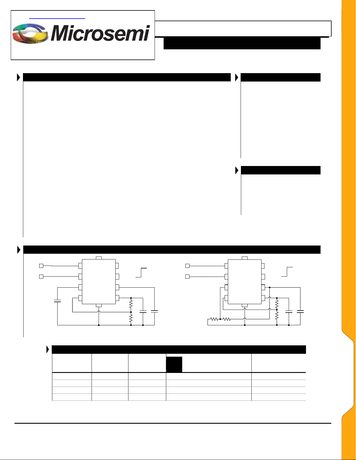
R1 = 13.0k
R2 = 10.0k
2.7V
R1
R2
Ω
Ω
3.0V
WWW.Microsemi .COM
Figure 1. Fixed / Adjustable Output Application
Resistor Table
5.0V
3.3V
R2
ADJ1
ADJ2
R1
VIN2
VIN1
N/C
EN1
EN2
VOUT1
VOUT2
GND
Figure 2 – Adjustable / Adjustable Output Application
VOUT1
R1 = 13.0k
R2 = 10.0kΩ
VOUT2
R1 = 11.3k
R2 = 10.0kΩ
2.7V
2.5V
R1
R2
Ω
Ω
A
A
A
A
P
P
P
P
P
P
P
P
L
L
L
L
I
I
I
I
C
C
C
C
A
A
A
A
T
T
T
T
I
I
I
I
O
O
O
O
N
N
N
N
S
S
S
S
Copyright © 2000
Rev. 1.0a, 2005-03-03
Microsemi
Linfinity Microelectronics Division
11861 Western Avenue, Garden Grove, CA. 92841, 714-898-8121, Fax: 714-893-2570
Page 6

LX8221
TM
OUTPUT VOLTAGE VS TEMPERATURE
1.185
1.18
1.175
1.17
1.165
OUTPUT VOLTAGE (V)
1.16
1.155
-50 -25 0 25 50 75 100 125
TEMPERATURE (°C)
®
Dual 150mA CMOS Low Dropout Regulator
DROPOUT VOLTAGE VS TEMPERATURE
350
325
300
275
250
225
200
175
150
125
100
75
50
-50 -25 0 25 50 75 100 125
IL=150mA
IL=100mA
TEMPERATURE ( °C)
WWW.Microsemi .COM
OUTPUT CURRENT VS SUPPLY VOLTAGE
0
-50
-100
-150
-200
-250
2.8 3.3 3.8 4.3 4.8 5.3 5.8 6.3
115°C
-40°C
25°C
85°C
SUPPLY V O LT AG E (V )
SHORT CIRCUIT CURRENT VS TEMPERATURE
-340
-350
-360
-370
-380
-390
-400
-410
-420
-430
-40 -25 0 25 85 100 115 125
5V
4V
3V
SUPPLY V O LTAG E (V )
0
PSRR VS FREQUENCY
PSRR VS FREQUENCY IN DROPOUT
0
50
100
0.1 1 10 100
Frequency (kHz)
Typical performance characteristics, unless otherwise specified are: CIN = C
Copyright © 2000
Rev. 1.0a, 2005-03-03
11861 Western Avenue, Garden Grove, CA. 92841, 714-898-8121, Fax: 714-893-2570
Linfinity Microelectronics Division
= 1µF, CBY = 470pF, VIN = V
OUT
Microsemi
50
100
0.1 1 10 100
Frequency (kHz)
= 2.5V, TA = 25°C, ENABLE is tied to V
OUT
IN.
Page 7
P
P
E
E
R
R
F
F
O
O
R
R
M
M
A
A
N
N
C
C
E
E

A
LX8221
TM
DU
10-Pin Plastic MSOP
G
D
B
C
®
PACKAGE DIMENSIONS
Dual 150mA CMOS Low Dropout Regulator
Dim
A 2.85 3.05 0.112 0.120
B 2.90 3.10 0.114 0.122
C - 1.10 - 0.043
D 0.16 0.31 0.006 0.0124
F 0.40 0.60 0.015 0.023
G 0.50 BSC 0.019 BSC
H 0.050 0.150 0.002 0.006
J 0.10 - 0.004 -
P 4.75 5.05 0.187 0.198
*LC - 0.10 - 0.004
*
Lead Coplanarity
J
M
ILLIMETERS
MIN MAX MIN MAX
I
NCHES
WWW.Microsemi .COM
F
P
H
Note: Dimensions do not include mold flash or protrusions; these shall not exceed 0.155mm(.006”) on any side. Lead dimension shall not
include solder coverage.
M
M
E
E
C
C
H
H
A
A
N
N
I
I
C
C
A
A
L
L
S
S
Copyright © 2000
Rev. 1.0a, 2005-03-03
Microsemi
Linfinity Microelectronics Division
11861 Western Avenue, Garden Grove, CA. 92841, 714-898-8121, Fax: 714-893-2570
Page 8

LX8221
TM
PRELIMINARY DATA – Information contained in this document is pre-production data, and is
proprietary to Linfinity. It may not be modified in any way without the express written consent of
Linfinity. Product referred to herein is not guaranteed to achieve preliminar y or production
status and product specifications, configurations, and availability may change at any time
®
Dual 150mA CMOS Low Dropout Regulator
NOTES
WWW.Microsemi .COM
N
N
O
O
T
T
E
E
S
S
Copyright © 2000
Rev. 1.0a, 2005-03-03
Microsemi
Linfinity Microelectronics Division
11861 Western Avenue, Garden Grove, CA. 92841, 714-898-8121, Fax: 714-893-2570
Page 9
 Loading...