

查询LX7201供应商
LX7201-xx
INTEGRATED PRODUCTS
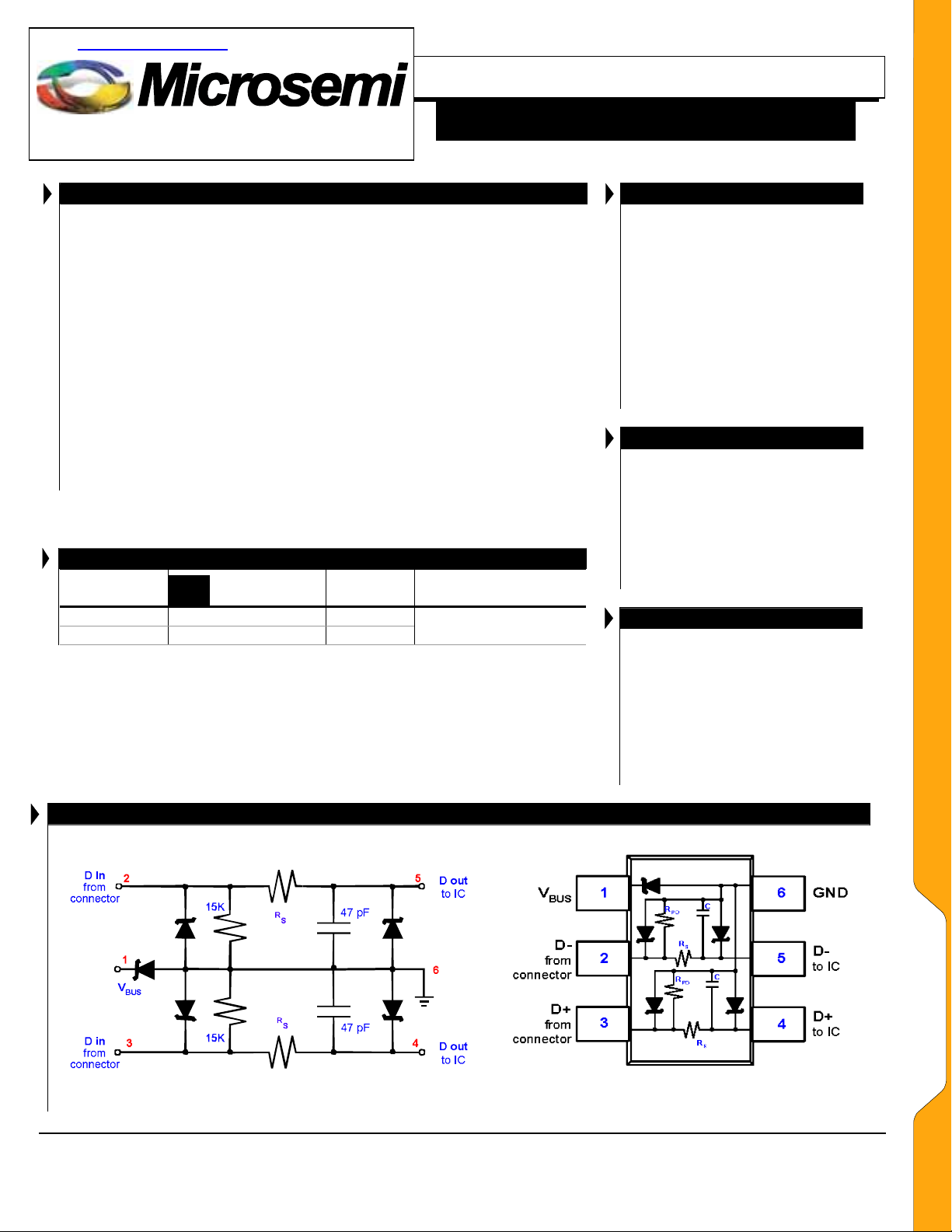
The LX7201 is an integrated
Universal Serial Bus (USB) line
termination device with an EMI filter
and ESD protection diodes. This
device offers a cost effective and
compact solution for one USB
downstream port. The USB
specification requires line termination
resistors on both the D+ and D- lines.
These resistors ensure signal integrity
by matching the cable impedance to
that of the differential driver. The
15KΩ pull-down resistors identify the
line as a downstream connection.
IMPORTANT: For the most current data, consult MICROSEMI’s website: http://www.microsemi.com
TJ (°C)
-40 to 125 LX7201-15ISF 115
-40 to 125 LX7201-22ISF 122
SF
DESCRIPTION
The 47 pF capacitor completes the
high frequency filter and controls the
edge rate of the USB signals. The
LX7201 protects both D+ and D- data
lines and the voltage bus from ESD.
The TVS protection diodes exceed the
requirements of IEC61000-4-2, level 4,
15kV (air discharge) and 8kV (contact
discharge). The integrated configuration
of the LX7201 minimizes board space
and allows for ideal placement near the
connector. The LX7201 is ideal for use
in USB hubs, peripherals and portable
appliances.
PACKAGE ORDER INFO
Plastic
6-Pin SOT23
Note: Append the letter “T” to the part number
For Tape & Reel Ordering
Package
Marking
PRODUCT HIGHLIGHT
Tape & Reel Quantity
(Reel Size)
EMI Filter & ESD Protection for Down Stream
USB Ports
P
3K (7inches)
RODUCTION DATA SHEET
KEY FEATURES
Bi-directional EMI/RFI Low-Pass
Filter
Line Termination with Integrated
ESD Protection
Low TVS Operating Voltage
(5.25V)
Low Leakage Current
Integrated Single Die
Construction
Available With 15 or 22Ω Series
Resistance
Crosses from Semtech STF201
APPLICATIONS
USB 1.1 and USB 2.0 Full
Speed Compliant
Peripherals
Printers
Monitors
Servers, Desktops and
Notebook Computers
Digital Cameras
BENEFITS
Filter response characterized up
to 6 GHz
<2dB insertion loss in the pass
band
>20dB attenuation in the 800-
900 MHz range
>12dB attenuation in the WLAN
frequencies of 2.4GHz and 5.0-
6.0 GHz
WWW.Microsemi .COM
Copyright © 2002
Rev. 1.0d, 2005-02-07
Circuit Diagram
Functional Schematic with Pin Out
Microsemi
11861 Western Avenue, Garden Grove, CA. 92841, 714-898-8121, Fax: 714-893-2570
Integrated Products Division
Page 1
L
L
X
X
7
7
2
2
0
0
1
1
-
-
X
X
X
X
LX7201-xx
INTEGRATED PRODUCTS
EMI Filter & ESD Protection for Down Stream
USB Ports
P
ABSOLUTE MAXIMUM RATINGS
Steady State Power .............................................................................100mW
ESD Air Discharge per IEC61000-4-2....................................................16kV
ESD Contact Discharge per IEC61000-4-2 ............................................10kV
Lead Soldering Temperature (10 Seconds).......................................... 260°C
Operating Temperature .........................................................-40°C to +125°C
RODUCTION DATA SHEET
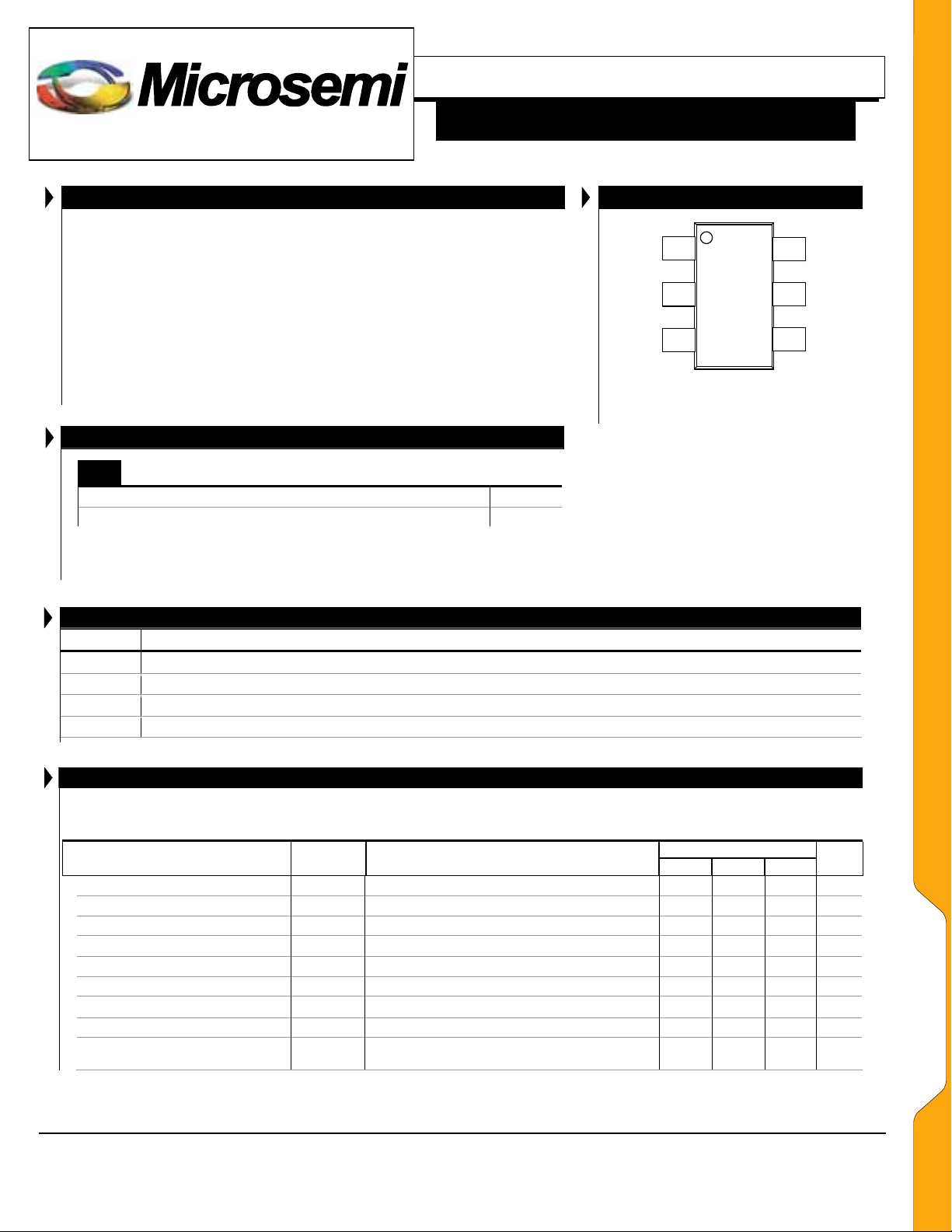
PACKAGE PIN OUT
BUS
D
1
2
IN
V
6
5
Storage Temperature Range..................................................-55°C to +150°C
Note: Exceeding these ratings could cause damage to the device. All voltages are with
respect to Ground. Currents are positive into, negative out of specified terminal
.
Plastic SOT23 6-Pin
SF
THERMAL RESISTANCE-JUNCTION TO CASE,
THERMAL RESISTANCE-JUNCTION TO AMBIENT,
Junction Temperature Calculation: TJ = TA + (PD x θJA).
numbers are guidelines for the thermal performance of the device/pc-board system. All
The θ
JA
of the above assume no ambient airflow.
THERMAL DATA
θ
JC
62 °C/W
θ
96 °C/W
JA
D
3
IN
SF P
ACKAGE
(Top View)
4
Name Description
VBUS Bus Voltage
DIN Data In
GND Ground
DOUT Data Out
Unless otherwise specified, the following specifications apply over the operating ambient temperature -40°C≤ T
otherwise noted.
Parameter Symbol Test Conditions
Stand-Off Voltage VRWM 5.25 V
Breakdown Voltage VBR IR = 1mA 6 V
Leakage Current I
Series Resistance (-15) RS Each Line 13.5 15 16.5
Series Resistance (-22) R
Temperature Coefficient of RS T
Pull Down Resistance R
Capacitor C Each Line 47 pF
Total Capacitance C
FUNCTIONAL PIN DESCRIPTION
ELECTRICAL CHARACTERISTICS
≤
+125°C except where
A
LX7201-xx
Min Typ Max
VRWM = 5.25V, T = 25°C 1 µA
R
Each Line 19.8 22 24.2
S
Each Line 200 ppm
COEFF
Each Line 13.5 15 16.5
PD
Between I/O Pins and Ground, Each Device
TOT
VR = 0V, f = 1MHz
54 60 66 pF
GND
D
OUT
D
OUT
Units
Ω
Ω
K
WWW.Microsemi .COM
E
E
L
Ω
L
E
E
C
C
T
T
R
R
I
I
C
C
A
A
L
L
S
S
Copyright © 2002
Rev. 1.0d, 2005-02-07
Microsemi
Integrated Products Division
11861 Western Avenue, Garden Grove, CA. 92841, 714-898-8121, Fax: 714-893-2570
Page 2

LX7201-xx
INTEGRATED PRODUCTS
EMI Filter & ESD Protection for Down Stream
USB Ports
P
RODUCTION DATA SHEET
APPLICATION CIRCUITS
WWW.Microsemi .COM
Host or Hub (downstream) port
LX7201
R
S
4
C
USB
Transceiver
5
R
PD
R
S
C
R
PD
6
GND
3
2
1
V
BUS
Peripheral (upstream) port
LX7202
V
BUS
16
R
PU
C
R
2
S
C
3
R
GND
5
Transceiver
4
S
USB
Figure 1 – Typical Application
The LX7201 meets the requirements of the USB v1.1
and USB 2.0 Full Speed specification for device
termination, EMI filtering and ESD protection. The R
resistor provides the proper signal termination; the 47pF
capacitor controls the signal rise and fall slew; the TVS
diodes protect the IC from ESD damage; and the total
capacitance and resistance creates a low pass filter
eliminating the high frequency energy from the circuit.
APPLICATION INFORMATION
FCC Part 15 sets limits for maximum allowable EM
emission and susceptibility. There are two types of
emissions. Conducted emissions with frequency of
emission of 0.45 to 30 MHz and Radiated emissions
with frequency of emission of 30 MHz to 40 GHz. All
digital computing devices including the peripheral
devices must comply. Examples of peripheral devices
include terminals, printers, external floppy disk drives
and other data storage devices, video monitors,
ELECTROMAGNETIC EMISSION AND SUSCEPTABILITY
Device Connection:
Voltage Supply (V
S
Ground is connected to Pin 6
D+ from the connector is routed to Pin 2 and out of Pin 5.
D- from the connector is routed to Pin 3 and out of Pin 4.
) is connected to Pin 1
BUS
keyboards, control cards, interface boards, external memory
expansion cards and other input/output devices that may or
may not contain digital circuitry. LX7201 is optimized to
minimize the radiated EMI which is the primary concern in
devices using USB. Refer to the typical filter response
curve for the attenuation characteristics of LX7201 over the
frequency range of 30KHz to 6GHz.
A
A
P
P
P
P
L
L
I
I
C
C
A
A
T
T
I
I
O
O
N
N
S
S
Copyright © 2002
Rev. 1.0d, 2005-02-07
Microsemi
Integrated Products Division
11861 Western Avenue, Garden Grove, CA. 92841, 714-898-8121, Fax: 714-893-2570
Page 3

LX7201-xx
INTEGRATED PRODUCTS
EMI Filter & ESD Protection for Down Stream
USB Ports
P
RODUCTION DATA SHEET
8KV Contact ESD
Ω
5.0V
Figure 2 – 8KV ESD input pulse as per IEC61000-4-2.
Vertical scale is equivalent to 5A/div.
CH1 S12 LOG 5dB / REF 0 dB
CHARACTERISTIC CURVES
1
40.0nsM
Figure 3 – Clamping Characteristics when device subjected
CH1 S12 LOG 20dB / REF 0 dB
Ω
5.0V
to an 8 KV ESD pulse.
MCh1
40.0ns
WWW.Microsemi .COM
START 0.030 000 MHz STOP 6 000.000 000 MHz
Figure 4 – Frequency response curve. Low insertion loss in
the pass band and -20dB attenuation at 800-900
MHz. Better than -10dB attenuation at the WLAN
frequencies of 2.4 and 5.0-6.0 GHz.
Copyright © 2002
Rev. 1.0d, 2005-02-07
11861 Western Avenue, Garden Grove, CA. 92841, 714-898-8121, Fax: 714-893-2570
START 0.030 000 MHz STOP 6 000.000 000 MHz
Figure 5 – Analog Crosstalk between the two datalines D-
Microsemi
Integrated Products Division
and D+
Page 4
C
C
H
H
A
A
R
R
T
T
S
S

LX7201-xx
INTEGRATED PRODUCTS
EMI Filter & ESD Protection for Down Stream
USB Ports
P
RODUCTION DATA SHEET
SF
6-Pin SOT-23 Package
D
G
PACKAGE DIMENSIONS
Dim
A 0.90 1.30 0.035 0.051
M
ILLIMETERS
I
MIN MAX MIN MAX
NCHES
WWW.Microsemi .COM
A1 0.90 1.45 0.035 0.057
B 0.25 0.50 0.010 0.020
C 0.09 0.20 0.004 0.008
H
E
D 2.80 3.10 0.110 0.122
E 1.50 1.75 0.059 0.069
F 0.95 BSC 0.038 BSC
G 1.90 BSC 0.075 BSC
H 2.60 3.00 0.102 0.118
I 0.35 0.55 0.014 0.022
A1
B
F
A
J
I
C
K
J 0.00 0.15 0.000 0.006
K 10° MAX 10° MAX
Note:
1. Dimensions do not include mold flash or protrusions;
these shall not exceed 0.155mm(.006”) on any side.
Lead dimension shall not include solder coverage.
Recommended Footprint
C (ref)
Copyright © 2002
Rev. 1.0d, 2005-02-07
X
M
ILLIMETERS
Dim
Y
C - 2.40 - 0.094
MIN MAX MIN MAX
I
D - 1.90 - 0.074
E - 0.95 - 0.037
X - 0.70 - 0.028
Y - 1.00 - 0.039
E (ref)
D (ref)
Microsemi
11861 Western Avenue, Garden Grove, CA. 92841, 714-898-8121, Fax: 714-893-2570
Integrated Products Division
NCHES
M
M
E
E
C
C
H
H
A
A
N
N
I
I
C
C
A
A
L
L
S
S
Page 5

LX7201-xx
INTEGRATED PRODUCTS
EMI Filter & ESD Protection for Down Stream
USB Ports
P
RODUCTION DATA SHEET
NOTES
WWW.Microsemi .COM
Copyright © 2002
Rev. 1.0d, 2005-02-07
PRODUCTION DATA – Information contained in this document is proprietary to
Microsemi and is current as of publication date. This document may not be modified in
any way without the express written consent of Microsemi. Product processing does not
necessarily include testing of all parameters. Microsemi reserves the right to change the
configuration and performance of the product and to discontinue product at any time.
Microsemi
11861 Western Avenue, Garden Grove, CA. 92841, 714-898-8121, Fax: 714-893-2570
Integrated Products Division
Page 6
N
N
O
O
T
T
E
E
S
S
 Loading...