

Page 1

IGLOO PLUS Starter Kit
User’s Guide
Page 2

Page 3

IGLOO PLUS Starter Kit User’s Guide
Table of Contents
Introduction . . . . . . . . . . . . . . . . . . . . . . . . . . . . . . . . . . . . . . . . . . . . . . . . . . . . . . . . . . . . . . . . . . . . . . 5
IGLOO PLUS Starter Kit Contents . . . . . . . . . . . . . . . . . . . . . . . . . . . . . . . . . . . . . . . . . . . . . . . . . . . . . . . . . . . . . . 5
1 Board Components and Settings . . . . . . . . . . . . . . . . . . . . . . . . . . . . . . . . . . . . . . . . . . . . . . . . . . . . . . 7
Board Description . . . . . . . . . . . . . . . . . . . . . . . . . . . . . . . . . . . . . . . . . . . . . . . . . . . . . . . . . . . . . . . . . . . . . . . . . . 7
IGLOO PLUS Board Stackup . . . . . . . . . . . . . . . . . . . . . . . . . . . . . . . . . . . . . . . . . . . . . . . . . . . . . . . . . . . . . . . . . . 8
Connectors, Jumpers, and Switch Settings . . . . . . . . . . . . . . . . . . . . . . . . . . . . . . . . . . . . . . . . . . . . . . . . . . . . . . 11
2 FPGA Description. . . . . . . . . . . . . . . . . . . . . . . . . . . . . . . . . . . . . . . . . . . . . . . . . . . . . . . . . . . . . . . . . 15
Key Features of AGLP125-CSG289 . . . . . . . . . . . . . . . . . . . . . . . . . . . . . . . . . . . . . . . . . . . . . . . . . . . . . . . . . . . 15
Power and Ground Pins . . . . . . . . . . . . . . . . . . . . . . . . . . . . . . . . . . . . . . . . . . . . . . . . . . . . . . . . . . . . . . . . . . . . . 16
JTAG Pins . . . . . . . . . . . . . . . . . . . . . . . . . . . . . . . . . . . . . . . . . . . . . . . . . . . . . . . . . . . . . . . . . . . . . . . . . . . . . . . 20
Decaps and Ground Post Schematics . . . . . . . . . . . . . . . . . . . . . . . . . . . . . . . . . . . . . . . . . . . . . . . . . . . . . . . . . . 21
3 Power . . . . . . . . . . . . . . . . . . . . . . . . . . . . . . . . . . . . . . . . . . . . . . . . . . . . . . . . . . . . . . . . . . . . . . . . . . 23
Power Modes . . . . . . . . . . . . . . . . . . . . . . . . . . . . . . . . . . . . . . . . . . . . . . . . . . . . . . . . . . . . . . . . . . . . . . . . . . . . . 24
Battery . . . . . . . . . . . . . . . . . . . . . . . . . . . . . . . . . . . . . . . . . . . . . . . . . . . . . . . . . . . . . . . . . . . . . . . . . . . . . . . . . . 25
Potentiometer and Voltage-Sweep . . . . . . . . . . . . . . . . . . . . . . . . . . . . . . . . . . . . . . . . . . . . . . . . . . . . . . . . . . . . 25
Current Measurement . . . . . . . . . . . . . . . . . . . . . . . . . . . . . . . . . . . . . . . . . . . . . . . . . . . . . . . . . . . . . . . . . . . . . . 26
4 Operation of Board Components . . . . . . . . . . . . . . . . . . . . . . . . . . . . . . . . . . . . . . . . . . . . . . . . . . . . . 29
Clock Oscillator . . . . . . . . . . . . . . . . . . . . . . . . . . . . . . . . . . . . . . . . . . . . . . . . . . . . . . . . . . . . . . . . . . . . . . . . . . . 29
Reset . . . . . . . . . . . . . . . . . . . . . . . . . . . . . . . . . . . . . . . . . . . . . . . . . . . . . . . . . . . . . . . . . . . . . . . . . . . . . . . . . . . 29
Flash*Freeze Mode . . . . . . . . . . . . . . . . . . . . . . . . . . . . . . . . . . . . . . . . . . . . . . . . . . . . . . . . . . . . . . . . . . . . . . . . 30
Push-Button Switches . . . . . . . . . . . . . . . . . . . . . . . . . . . . . . . . . . . . . . . . . . . . . . . . . . . . . . . . . . . . . . . . . . . . . . 37
.DIP Switches . . . . . . . . . . . . . . . . . . . . . . . . . . . . . . . . . . . . . . . . . . . . . . . . . . . . . . . . . . . . . . . . . . . . . . . . . . . . . 38
User LEDs . . . . . . . . . . . . . . . . . . . . . . . . . . . . . . . . . . . . . . . . . . . . . . . . . . . . . . . . . . . . . . . . . . . . . . . . . . . . . . . 39
I/O Test Pins . . . . . . . . . . . . . . . . . . . . . . . . . . . . . . . . . . . . . . . . . . . . . . . . . . . . . . . . . . . . . . . . . . . . . . . . . . . . . 40
OLED . . . . . . . . . . . . . . . . . . . . . . . . . . . . . . . . . . . . . . . . . . . . . . . . . . . . . . . . . . . . . . . . . . . . . . . . . . . . . . . . . . . 41
Interface Connector . . . . . . . . . . . . . . . . . . . . . . . . . . . . . . . . . . . . . . . . . . . . . . . . . . . . . . . . . . . . . . . . . . . . . . . . 42
USB-to-UART Interface . . . . . . . . . . . . . . . . . . . . . . . . . . . . . . . . . . . . . . . . . . . . . . . . . . . . . . . . . . . . . . . . . . . . . 42
SPI Flash . . . . . . . . . . . . . . . . . . . . . . . . . . . . . . . . . . . . . . . . . . . . . . . . . . . . . . . . . . . . . . . . . . . . . . . . . . . . . . . . 43
Low-Cost Programming Stick (LCPS) . . . . . . . . . . . . . . . . . . . . . . . . . . . . . . . . . . . . . . . . . . . . . . . . . . . . . . . . . . 44
5 Programming . . . . . . . . . . . . . . . . . . . . . . . . . . . . . . . . . . . . . . . . . . . . . . . . . . . . . . . . . . . . . . . . . . . . 49
6 IGLOO PLUS Board Demo . . . . . . . . . . . . . . . . . . . . . . . . . . . . . . . . . . . . . . . . . . . . . . . . . . . . . . . . . 51
Demos Included in the Starter Kit . . . . . . . . . . . . . . . . . . . . . . . . . . . . . . . . . . . . . . . . . . . . . . . . . . . . . . . . . . . . . 51
Powering Up the Board . . . . . . . . . . . . . . . . . . . . . . . . . . . . . . . . . . . . . . . . . . . . . . . . . . . . . . . . . . . . . . . . . . . . . 51
Getting Started with the IGLOO PLUS Starter Kit Demo Design . . . . . . . . . . . . . . . . . . . . . . . . . . . . . . . . . . . . . . 51
A Resources . . . . . . . . . . . . . . . . . . . . . . . . . . . . . . . . . . . . . . . . . . . . . . . . . . . . . . . . . . . . . . . . . . . . . . 55
B List of Changes . . . . . . . . . . . . . . . . . . . . . . . . . . . . . . . . . . . . . . . . . . . . . . . . . . . . . . . . . . . . . . . . . . 57
Revision 1 3
Page 4

Table of Contents
C Product Support . . . . . . . . . . . . . . . . . . . . . . . . . . . . . . . . . . . . . . . . . . . . . . . . . . . . . . . . . . . . . . . . . . 59
Customer Service . . . . . . . . . . . . . . . . . . . . . . . . . . . . . . . . . . . . . . . . . . . . . . . . . . . . . . . . . . . . . . . . . . . . . . . . . 59
Customer Technical Support Center . . . . . . . . . . . . . . . . . . . . . . . . . . . . . . . . . . . . . . . . . . . . . . . . . . . . . . . . . . . 59
Technical Support . . . . . . . . . . . . . . . . . . . . . . . . . . . . . . . . . . . . . . . . . . . . . . . . . . . . . . . . . . . . . . . . . . . . . . . . . 59
Website . . . . . . . . . . . . . . . . . . . . . . . . . . . . . . . . . . . . . . . . . . . . . . . . . . . . . . . . . . . . . . . . . . . . . . . . . . . . . . . . . 59
Contacting the Customer Technical Support Center . . . . . . . . . . . . . . . . . . . . . . . . . . . . . . . . . . . . . . . . . . . . . . . 59
ITAR Technical Support . . . . . . . . . . . . . . . . . . . . . . . . . . . . . . . . . . . . . . . . . . . . . . . . . . . . . . . . . . . . . . . . . . . . . 60
Index . . . . . . . . . . . . . . . . . . . . . . . . . . . . . . . . . . . . . . . . . . . . . . . . . . . . . . . . . . . . . . . . . . . . . . . . . . 61
4 Revision 1
Page 5

Introduction
IGLOO PLUS Starter Kit Contents
The RoHS-compliant, environmentally friendly IGLOO® PLUS Starter Kit is packaged in a recyclable
cardboard box made from recycled materials. This development kit includes an on-board programmer
and demonstrates the ultra-low power of Microsemi® IGLOO PLUS devices. Ta bl e 1 lists the contents of
the box.
Table 1 • IGLOO PLUS Starter Kit Contents
Quantity Contents
1 IGLOO PLUS board with AGLP125 IGLOO PLUS field programmable gate array (FPGA)
1 Programmer for use with IGLOO PLUS board
1 5 V power supply
2 USB 2.0 high-speed cables
1 Packet of jumpers
®
1 Microsemi Libero
1 Quickstart Guide
System-on-Chip (SoC) software DVD
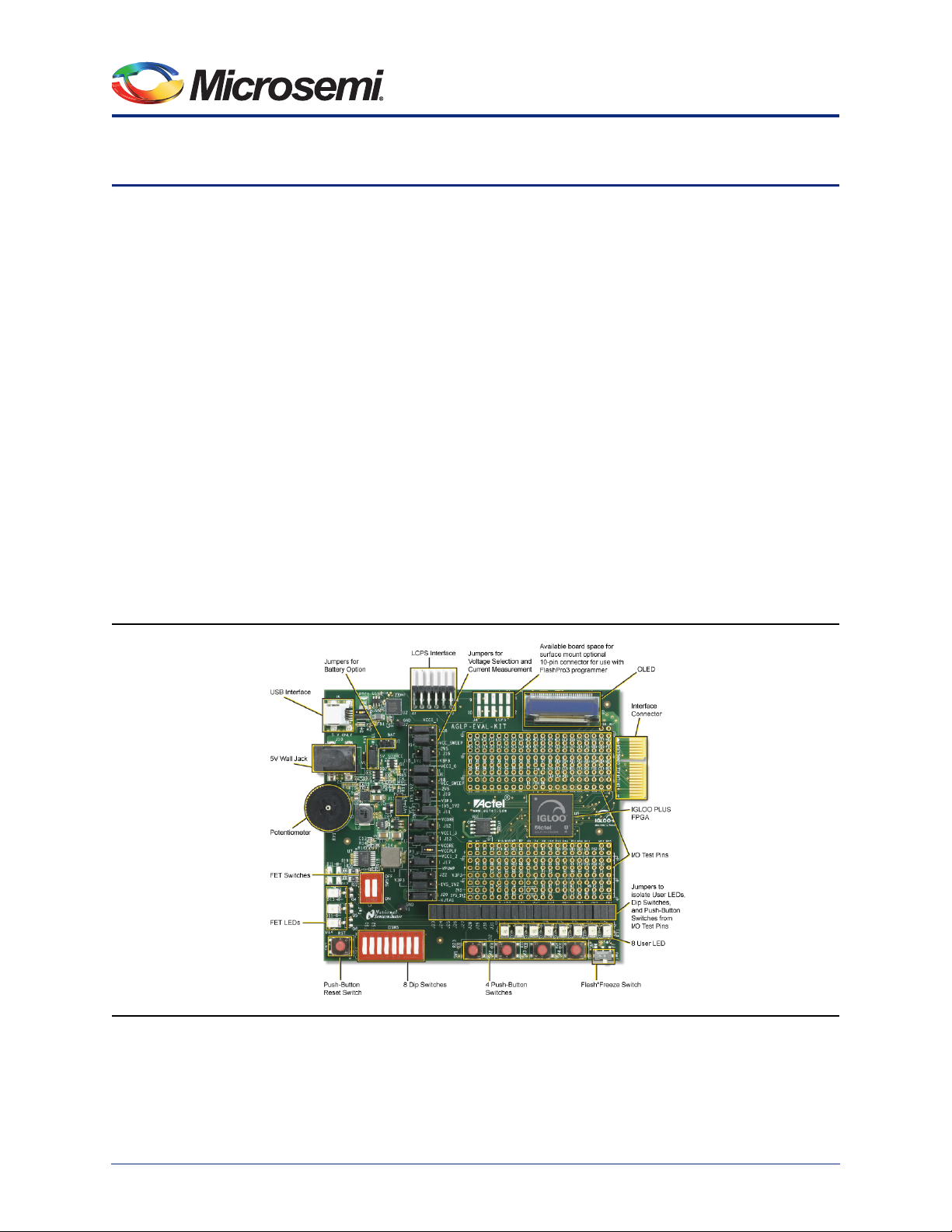
Figure 1 • IGLOO PLUS Starter Kit Board
Revision 1 5
Page 6

Page 7
1 – Board Components and Settings
This chapter describes the components and settings for the IGLOO PLUS Starter Kit Board.
Board Description
The IGLOO PLUS Starter Kit board is intended to provide a low-cost system platform for evaluating
IGLOO PLUS (AGLP) technology, such as low power, I/O state preservation during Flash*Freeze mode,
and Schmitt Triggered I/Os. Other advanced features include the ability to use the FPGA I/Os of the
Expansion Header as hot-swappable and the Schmitt Triggered FPGA inputs for improved noise
immunity.
This evaluation board enables you to measure power consumption (dynamic, static, and Flash*Freeze
modes) with the core operating between 1.2 V and 1.5 V. When using the board in conjunction with the
Microsemi power analysis tools, you will have a clear picture of application power consumption at each
stage in your design. In addition, the Libero SoC tool suite now includes power-driven layout (PDL),
which can reduce the power consumption of designs up to 30 percent.
The evaluation board has a small form factor, measuring 3.7 inches by 4 inches, and supports an
AGLP125 IGLOO PLUS device in the 14 mm × 14 mm CSG289 package. All components used on the
board, such as LEDs, reset (µA range), and oscillator, are low-power components. Also included on the
evaluation board is a USB-to-UART interface to allow HyperTerminal on a PC to communicate with the
IGLOO PLUS device on the board.
The top of the board has a programming stick header which allows the low-cost programming stick
LCPS) to be attached to the board for programming the IGLOO PLUS AGLP125-CSG289 device
(Figure 1-1). FPGA I/Os have been wired to test pin pads on the board for debug and expandability.
Figure 1-1 • IGLOO PLUS Starter Kit Board
Note: The clock oscillator for the IGLOO PLUS Starter Kit Board is behind the board.
Revision 1 7
Page 8

Board Components and Settings
IGLOO PLUS Board Stackup
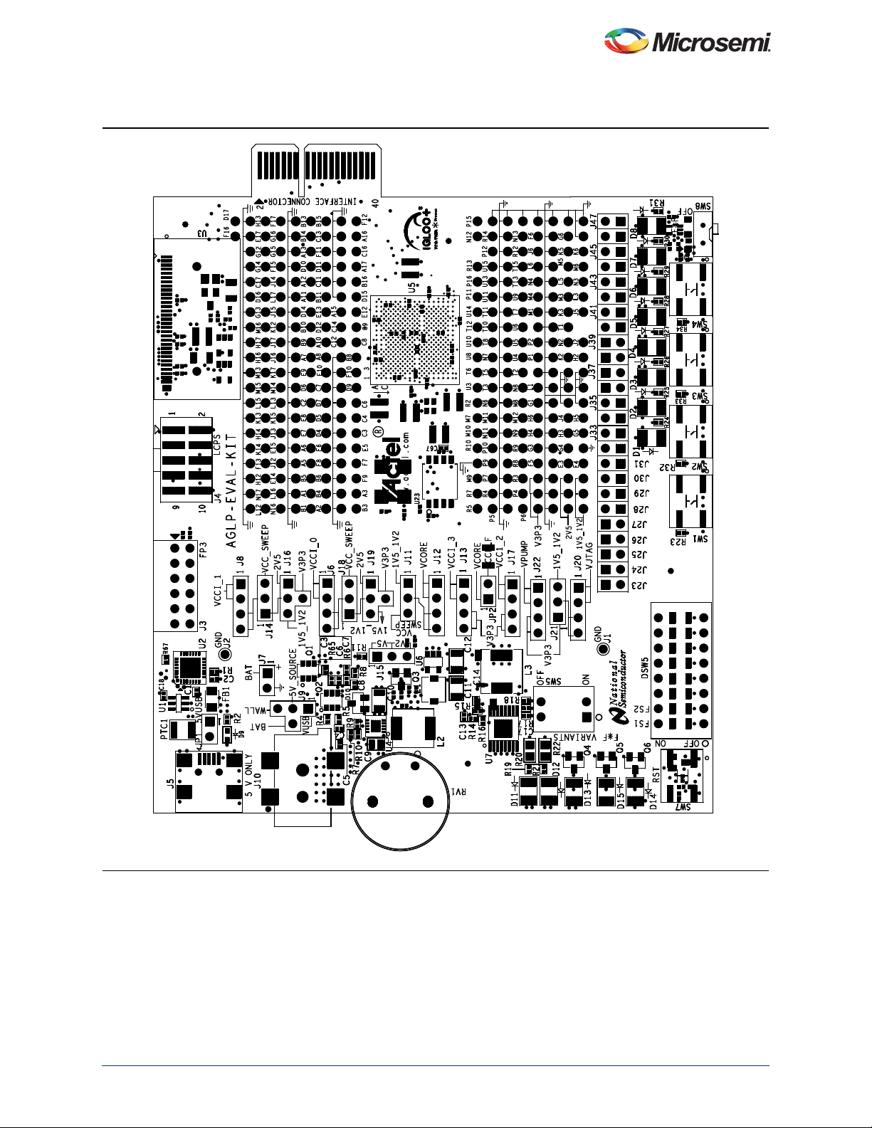
The IGLOO PLUS board is built on a 10-layer PCB. Figure 1-1 and Figure 1-1 on page 7 show the top
(L1) and bottom (L10) silkscreens. The full PCB design layout is provided on the Microsemi SoC
Products Group website, on the IGLOO PLUS Starter Kit page:
www.microsemi.com/soc/products/hardware/devkits_boards/iglooplus_starter.aspx. To view the PCB
design layout files, you can use the Allegro Free Physical Viewer, which can be downloaded from the
Cadence Allegro Downloads page.
• Top Signal (Figure 1-1 on page 7)
•GND 1
•Signal
•GND 2
•PWR 1
•PWR 2
•GND 3
•Signal
•GND 4
• Bottom Signal (Figure 1-2 on page 9)
8 Revision 1
Page 9
IGLOO PLUS Starter Kit User’s Guide
Figure 1-2 • IGLOO PLUS Top Silkscreen (L1)
Revision 1 9
Page 10
Board Components and Settings
Figure 1-3 • IGLOO PLUS Bottom Silkscreen (L10)
10 Revision 1
Page 11
IGLOO PLUS Starter Kit User’s Guide
Connectors, Jumpers, and Switch Settings
Recommended default jumper settings are defined in Table 1-1. The voltage selection jumpers are
highlighted in grey. Connect jumpers in the default settings described in Ta bl e 1-1 to enable the preprogrammed demo design to function correctly.
Table 1-1 • Jumper and Connector Settings
Jumper Default Setting Comment
J1 Ground post header
J2 Ground post header
J3 LC JTAG header for programmer
J4 JTAG header
J5 USB mini receptacle
J6 Pin 2-3 Remove jumper to disconnect VCCI_0 power
J7 Remove Remove jumper to disconnect external battery source
J8 Pin 2-3 Remove jumper to disconnect VCCI_1 power
J9 Pin 1-4 Select WALL, BAT, VUSB for 5V_SOURCE
Pin 1-4 = VUSB
Pin 2-4 = BAT
Pin 3-4 = WALL
J10 5 V Brick
J11 Pin 1-2 Select VCC or VCC_SWEEP for VCORE
Pin 1-2 = VCC
Pin 3-2 = VCC_SWEEP
J12 Pin 2-3 Current measurement header for VCORE
J13 Pin 2-3 Current measurement header for VCCI_3
J14 Pin 1-2 Select VCC or VCC_SWEEP for VCCI_1
Pin 1-2 = VCC
Pin 3-2 = VCC_SWEEP
J15 Pin 3-2 Select VJTAGENB or 3.3 V
Pin 3-2 = VJTAGENB
Pin 1-2 = 3.3 V
J16 Pin 2-4 Select 3.3 V, 1.5 / 1.2 V, or 2.5 V for VCCI_1
Pin 2-4 = 3.3 V
Pin 3-4 = 1.5 V or 1.2 V
Pin 1-4 = 2.5 V
J17 Pin 2-3 Current measurement header for VCCI_2
J18 Pin 1-2 Select VCC or VCC_SWEEP for VCCI_0
Pin 1-2 = VCC
Pin 3-2 = VCC_SWEEP
Revision 1 11
Page 12
Board Components and Settings
Table 1-1 • Jumper and Connector Settings (continued)
Jumper Default Setting Comment
J19 Pin 2-4 Select 3.3 V, 1.5 / 1.2 V, or 2.5 V for VCCI_0
Pin 2-4 = 3.3 V
Pin 3-4 = 1.5 V or 1.2 V
Pin 1-4 = 2.5 V
J20 Pin 2-3 Current measurement header for VJTAG
J21 Pin 1-2 Select 3.3 V or 1.5 / 1.2 V for VJTAG
Pin 1-2 = 3.3 V
Pin 2-3 = 1.5 V or 1.2 V
J22 Pin 2-3 Current measurement header for VPUMP
J23-J24 Pin 1-2 Remove each jumper to disconnect any of the 2 FET Switches[1:2] from
FPGA.
J23 = 3V3_SWITCH1
J24 = 3V3_SWITCH2
J25-J27 Pin 1-2 Remove each jumper to disconnect any of the 3 FET LEDs from FPGA.
J25 = FET_P1
J26 = FET_N
J27 = FET_P2
J28-J35 Pin 1-2 Remove each jumper to disconnect any of the 8 user DIP switches[1:8] from
FPGA.
J28 = D_SWITCH1
J29 = D_SWITCH2
J30 = D_SWITCH3
J31 = D_SWITCH4
J32 = D_SWITCH5
J33 = D_SWITCH6
J34 = D_SWITCH7
J35 = D_SWITCH8
J36-J39 Pin 1-2 Remove each jumper to disconnect any of the 4 push-button switches[1:4] from
FPGA.
J36 = SWITCH1
J37 = SWITCH2
J38 = SWITCH3
J39 = SWITCH4
J40-J47 Pin 1-2 Remove each jumper to disconnect any of the 8 user LEDs[1:8] from FPGA.
J42 = LED1
J41 = LED2
J40 = LED3
J47 = LED4
J46 = LED5
J45 = LED6
J44 = LED7
J43 = LED8
12 Revision 1
Page 13
IGLOO PLUS Starter Kit User’s Guide
Table 1-2 • Switch Settings
Switch Default Setting Comment
SW1–SW4 Push-button switches for SWITCH[1:4]
SW5 CLOSE Contains DIP switches for 3V3_SWITCH[1:2]
DSW5 CLOSE Contains DIP switches for D_SWITCH[1:8]
SW7 Push-button switch for system reset PBRESET_N
SW8 OFF Flash*Freeze: To enable Flash*Freeze mode, SW8 toward ON.
In Flash*Freeze mode, current consumption of FPGA goes below 50 µA.
Revision 1 13
Page 14

Page 15
2 – FPGA Description
The IGLOO PLUS board is populated with an IGLOO PLUS AGLP125-CSG289 FPGA.
Key Features of AGLP125-CSG289
• Low power
• 1.2 V to 1.5 V core voltage support for low power
• Supports single-voltage system operation
• 5 µW power consumption in Flash*Freeze mode
• Low-power active FPGA operation
• Flash*Freeze technology enables ultra-low power consumption while maintaining FPGA content
• Configurable hold previous state, tristate, HIGH, or LOW state per I/O in Flash*Freeze mode
• Easy entry to / exit from ultra-low-power Flash*Freeze mode
• Reprogrammable flash technology
• In-system programming (ISP) and security
• High-performance routing hierarchy
• Advanced I/O
• Selectable Schmitt trigger inputs
• Clock conditioning circuit (CCC) and PLL
• Embedded memory
Table 2-1 lists specifications for the AGLP125-CSG289 FPGA.
Table 2-1 • IGLOO PLUS AGLP125-CSG289 FPGA Features
Feature Specification
System Gates 125,000
Typical Equivalent Macrocells 1,024
VersaTiles (D-flip-flops) 3,120
Flash*Freeze Mode (Typical, µW) 16
RAM kbits (1,024 bits) 36
4,608-Bit Blocks 8
FlashROM (bits) 1 K
Secure (AES) ISP Yes
Integrated PLLs in CCCs 1
VersaNet Globals 18
I/O Banks 4
Maximum User I/Os 212
For further information, refer to the IGLOO PLUS datasheet:
www.microsemi.com/soc/documents/IGLOOPLUS_DS.pdf
Revision 1 15
Page 16
FPGA Description
VCCPLF
VCCIB0_1
B7
VCCIB0_2
B12
VCCIB0_3
C5
VCCIB0_4
E11
VCCIB1_1
E16
VCCIB1_2
H15
VCCIB1_3
L14
VCCIB1_4
M17
VCCIB2_1
N10
VCCIB2_2
P13
VCCIB2_3
R6
VCCIB2_4
T9
VCCIB3_1
E1
VCCIB3_2
F4
VCCIB3_3
J3
VCCIB3_4
M2
VCC1
L9
VCC2
G9
VCC3
J7
VCC4
J11
VCOMPLF
H1
VCCPLF
J1
GND1
A4
GND2
A9
GND3
A14
GND4
B2
GND5
B17
GND6
C10
GND7
C15
GND8
D3
GND9
D8
GND10
D13
GND11
F14
GND12
G2
GND13
G7
GND14
G8
GND15
G10
GND16
G11
GND17
G17
GND18
H7
GND19
H8
GND20
H9
GND21
H10
GND22
H11
GND23
J8
GND24
J9
GND25
J10
GND26
K1
GND27
K7
GND28
K8
GND29
K9
GND30
K10
GND31
K11
GND32
K16
GND33
L4
GND34
L7
GND35
L8
GND36
L10
GND37
L11
GND38
N5
GND39
N15
GND40
P3
GND41
P8
GND42
R1
GND43
R11
GND44
T4
GND45
T14
GND46
U2
GND47
U7
GND48
U12
SEC 5/6
AGLP125 CSG289
POWER
GND
U5E
AGLP125-CSG289
SEC 5/6
POWER
GND
U5E
Power and Ground Pins
Figure 2-1 shows the power and ground pins for AGLP125-CSG289.
Figure 2-1 • Power and Ground Pins for AGLP125-CSG289
16 Revision 1
Page 17
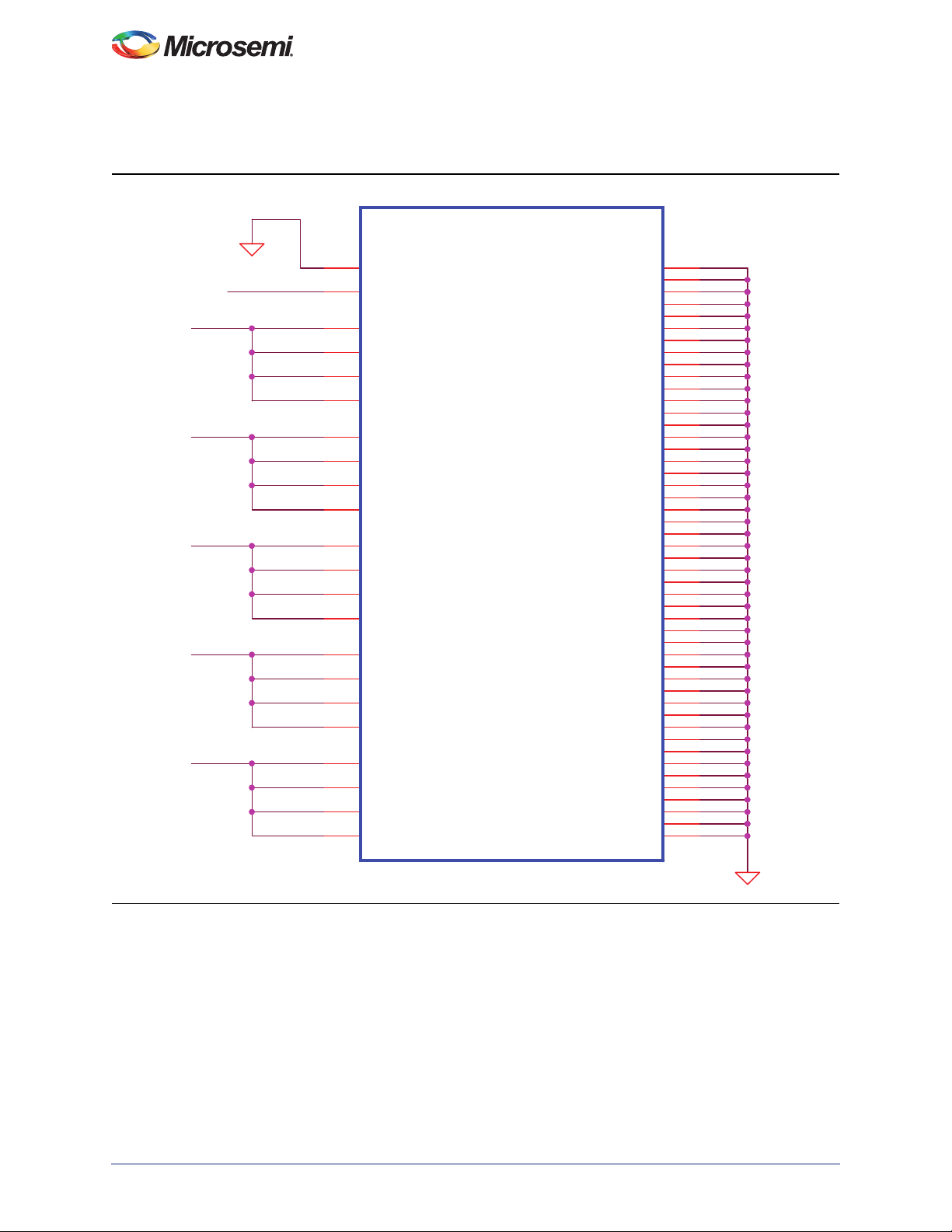
Bank I/O Signals
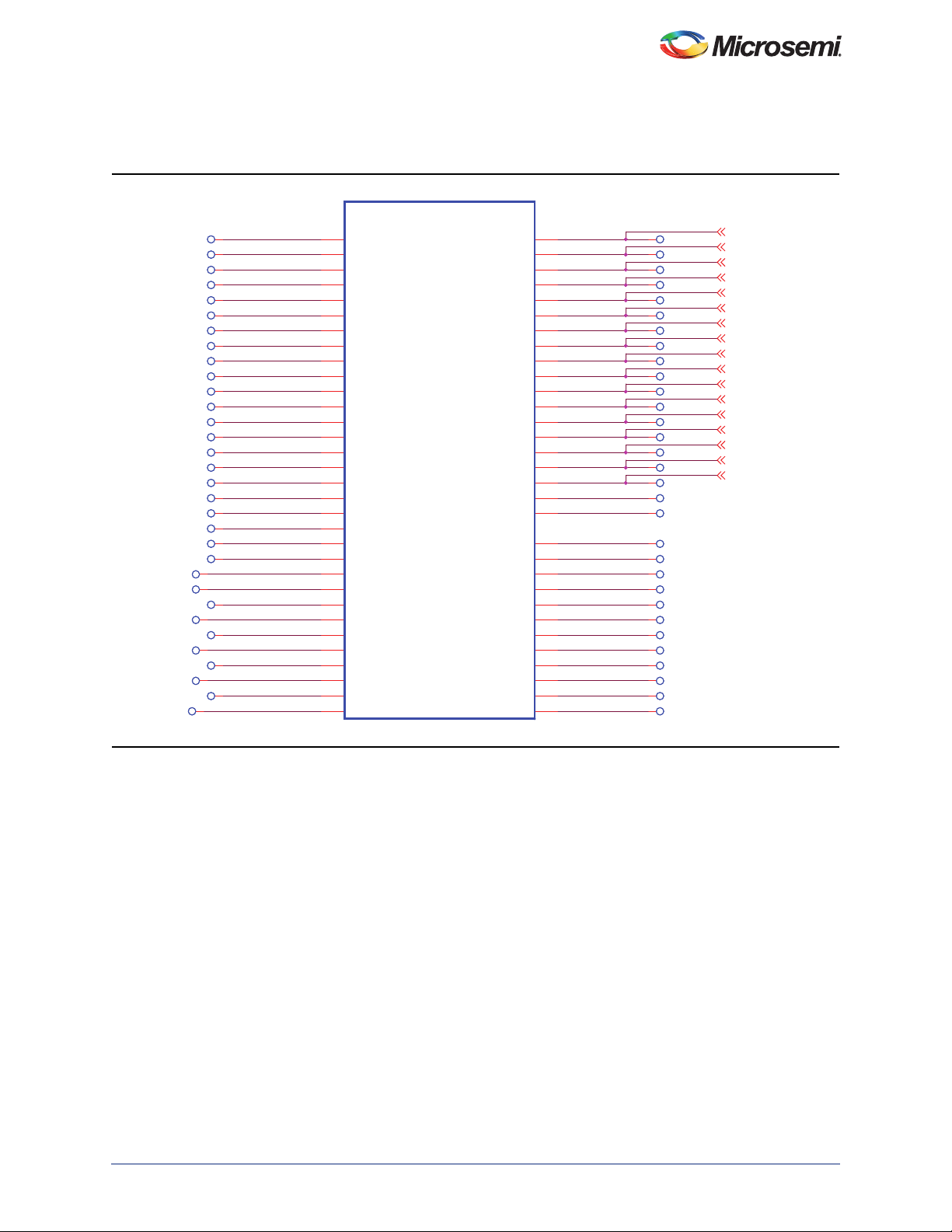
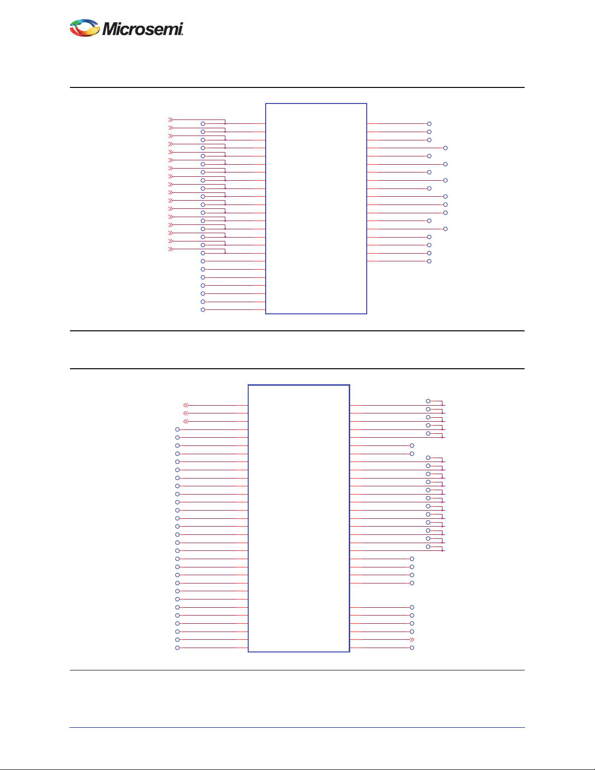
Figure 2-2 through Figure 2-5 on page 19 show the schematics for the bank I/O signals.
TP105TPTP105
TP112TPTP112
TP69TPTP69
TP71TPTP71
TP110TPTP110
TP85TPTP85
TP74TPTP74
TP86TPTP86
TP108TPTP108
TP106TPTP106
TP101TPTP101
TP120TPTP120
TP72TPTP72
TP70TPTP70
TP113TPTP113
TP87TPTP87
TP114TPTP114
TP121TPTP121
TP107TPTP107
TP73TPTP73
TP115TPTP115
TP75TPTP75
TP95TPTP95
TP122TPTP122
TP94TPTP94
TP123TPTP123
AGL_B0_PIN_B3
AGL_B0_PIN_D5
AGL_B0_PIN_A3
AGL_B0_PIN_C4
AGL_B0_PIN_D6
AGL_B0_PIN_A2
AGL_B0_PIN_E6
AGL_B0_PIN_B4
AGL_B0_PIN_F7
AGL_B0_PIN_B5
AGL_B0_PIN_E7
AGL_B0_PIN_C6
AGL_B0_PIN_D7
AGL_B0_PIN_A5
AGL_B0_PIN_F8
AGL_B0_PIN_B6
AGL_B0_PIN_E8
AGL_B0_PIN_C7
AGL_B0_PIN_A6
AGL_B0_PIN_F9
AGL_B0_PIN_A7
AGL_B0_PIN_C8
AGL_B0_PIN_B8
AGL_B0_PIN_F10
AGL_B0_PIN_A8
AGL_B0_PIN_B9
AGL_B0_PIN_E9
AGL_B0_PIN_C9
AGL_B0_PIN_D9
AGL_B0_PIN_A10
AGL_B0_PIN_E10
AGL_B0_PIN_B10
TP
TP
TP
TP
TP
TP
TP
TP
TP
TP
TP
TP
TP
TP
TP
TP
TP
TP
TP
TP
TP
TP
TP207TPTP207
TP
TP222TPTP222
TP
TP
TP239TPTP239
TP
TP
TP240TPTP240
TP
TP
TP247TPTP247
TP
TP
TP236TPTP236
TP
AGLP125 CSG289
B3
IO06RSB0
D5
IO07RSB0
A3
IO08RSB0
C4
IO09RSB0
D6
IO10RSB0
A2
IO11RSB0
E6
IO12RSB0
B4
IO13RSB0
F7
IO14RSB0
B5
IO15RSB0
E7
IO16RSB0
C6
IO17RSB0
D7
IO18RSB0
A5
IO19RSB0
F8
IO20RSB0
B6
IO21RSB0
E8
IO22RSB0
C7
IO23RSB0
A6
IO24RSB0
F9
IO25RSB0
A7
IO26RSB0
C8
IO27RSB0
B8
IO28RSB0
F10
IO29RSB0
A8
IO30RSB0
B9
IO31RSB0
E9
IO32RSB0
C9
IO33RSB0
D9
IO34RSB0
A10
IO35RSB0
E10
IO36RSB0
B10
IO37RSB0
U5A
U5A
SEC 1/6
SEC 1/6
BANK0
BANK0
AGLP125-CSG289
IO38RSB0
IO39RSB0
IO40RSB0
IO41RSB0
IO42RSB0
IO43RSB0
IO44RSB0
IO45RSB0
IO46RSB0
IO47RSB0
IO48RSB0
IO49RSB0
IO50RSB0
IO51RSB0
IO52RSB0
IO53RSB0
IO54RSB0
IO55RSB0
IO56RSB0
GAA0/IO00RSB0
GAA1/IO01RSB0
GAB0/IO02RSB0
GAB1/IO03RSB0
GAC0/IO04RSB0
GAC1/IO05RSB0
GBA0/IO61RSB0
GBA1/IO62RSB0
GBB0/IO59RSB0
GBB1/IO60RSB0
GBC0/IO57RSB0
GBC1/IO58RSB0
A11
B11
A12
D10
A13
C11
B13
C12
B14
D11
A15
B15
C13
F11
C14
F12
A16
D12
E12
C2
B1
D4
A1
C3
E5
C16
D15
D14
E13
A17
B16
IGLOO PLUS Starter Kit User’s Guide
GPIOA_1 {3}
GPIOA_3 {3}
GPIOA_5 {3}
GPIOA_7 {3}
GPIOA_9 {3}
GPIOA_13 {3}
GPIOA_15 {3}
GPIOA_17 {3}
GPIOA_19 {3}
GPIOA_21 {3}
GPIOA_23 {3}
GPIOA_25 {3}
GPIOA_27 {3}
GPIOA_29 {3}
GPIOA_31 {3}
GPIOA_33 {3}
GPIOA_35 {3}
AGL_B0_PIN_D12
AGL_B0_PIN_E12
AGL_B0_PIN_C2
AGL_B0_PIN_B1
AGL_B0_PIN_D4
AGL_B0_PIN_A1
AGL_B0_PIN_C3
AGL_B0_PIN_E5
AGL_B0_PIN_C16
AGL_B0_PIN_D15
AGL_B0_PIN_D14
AGL_B0_PIN_E13
AGL_B0_PIN_A17
AGL_B0_PIN_B16
TP96TPTP96
TP116TPTP116
TP79TPTP79
TP124TPTP124
TP117TPTP117
TP77TPTP77
TP97TPTP97
TP89TPTP89
TP80TPTP80
TP78TPTP78
TP118TPTP118
TP98TPTP98
TP111TPTP111
TP76TPTP76
TP109TPTP109
TP103TPTP103
TP81TPTP81
TP93TPTP93
TP92TPTP92
TP102TPTP102
TP22TPTP22
TP90TPTP90
TP68TPTP68
TP83TPTP83
TP91TPTP91
TP82TPTP82
TP84TPTP84
TP88TPTP88
TP100TPTP100
TP99TPTP99
TP119TPTP119
TP
TP
TP
TP
TP
TP
TP
TP
TP
TP
TP
TP
TP
TP
TP
TP
TP
TP
TP
TP
TP
TP
TP
TP
TP
TP
TP
TP
TP
TP
TP
Figure 2-2 • Bank 0 I/O Signals for AGLP125-CSG289
Revision 1 17
Page 18
FPGA Description
{3}
{3}
{3}
{3}
GPIOA_2{3}
GPIOA_4
GPIOA_6{3}
GPIOA_8{3}
GPIOA_10
GPIOA_12{3}
GPIOA_16{3}
GPIOA_18{3}
GPIOA_20{3}
GPIOA_22
GPIOA_24{3}
GPIOA_26{3}
GPIOA_28{3}
GPIOA_30
GPIOA_32{3}
GPIOA_34{3}
GPIOA_36{3}
U5B
U5B
AGLP125 CSG289
SEC 2/6
TP38TPTP38
TP
TP45TPTP45
TP
TP44TPTP44
TP
TP40TPTP40
TP
TP26TPTP26
TP
TP27TPTP27
TP
TP33TPTP33
TP
TP46TPTP46
TP
TP17TPTP17
TP
TP25TPTP25
TP
TP28TPTP28
TP
TP47TPTP47
TP
TP32TPTP32
TP
TP36TPTP36
TP
TP23TPTP23
TP
TP37TPTP37
TP
TP35TPTP35
TP
AGL_B1_PIN_L16
TP49TPTP49
TP
AGL_B1_PIN_K15
TP21TPTP21
TP
AGL_B1_PIN_K13
TP34TPTP34
TP
AGL_B1_PIN_K14
TP16TPTP16
TP
AGL_B1_PIN_M16
TP30TPTP30
TP
AGL_B1_PIN_M15
TP18TPTP18
TP
TP41TPTP41
AGL_B1_PIN_L15
TP
G13
IO64RSB1
D16
IO66RSB1
C17
IO68RSB1
G14
IO69RSB1
D17
IO70RSB1
F16
IO71RSB1
G12
IO72RSB1
E17
IO73RSB1
H13
IO74RSB1
F15
IO75RSB1
G16
IO76RSB1
F17
IO77RSB1
G15
IO78RSB1
K12
IO88RSB1
J15
IO89RSB1
J14
IO90RSB1
L17
IO91RSB1
L16
IO92RSB1
K15
IO93RSB1
K13
IO94RSB1
K14
IO95RSB1
M16
IO96RSB1
M15
IO97RSB1
L15
IO98RSB1
SEC 2/6
BANK1
BANK1
AGLP125-CSG289
GBA2/IO63RSB1
GBB2/IO65RSB1
GBC2/IO67RSB1
GCA0/IO84RSB1
GCA1/IO83RSB1
GCA2/IO85RSB1
GCB0/IO82RSB1
GCB1/IO81RSB1
GCB2/IO86RSB1
GCC0/IO80RSB1
GCC1/IO79RSB1
GCC2/IO87RSB1
GDA0/IO104RSB1
GDA1/IO103RSB1
GDB0/IO102RSB1
GDB1/IO101RSB1
GDC0/IO100RSB1
GDC1/IO99RSB1
E14
E15
F13
H14
J17
H16
J16
J13
J12
H17
H12
K17
M14
M13
N16
L13
N17
L12
AGL_B1_PIN_E14
AGL_B1_PIN_E15
AGL_B1_PIN_F13
AGL_B1_PIN_H14
AGL_B1_PIN_J17
AGL_B1_PIN_H16
AGL_B1_PIN_J16
AGL_B1_PIN_J13
AGL_B1_PIN_J12
AGL_B1_PIN_H17
AGL_B1_PIN_H12
AGL_B1_PIN_K17
AGL_B1_PIN_M14
AGL_B1_PIN_M13
AGL_B1_PIN_N16
AGL_B1_PIN_L13
AGL_B1_PIN_N17
AGL_B1_PIN_L12
TP39TPTP39
TP104TPTP104
TP42TPTP42
TP29TPTP29
TP48TPTP48
TP43TPTP43
TP20TPTP20
TP50TPTP50
TP24TPTP24
TP31TPTP31
TP19TPTP19
TP
TP
TP
TP226TPTP226
TP
TP210TPTP210
TP
TP223TPTP223
TP
TP208TPTP208
TP142TPTP142
TP162TPTP162
TP
TP183TPTP183
TP
TP
TP
TP
TP
TP
TP
TP
TP
TP
TP
Figure 2-3 • Bank 1 I/O Signals for AGLP125-CSG289
AGLP125 CSG289
P14
N14
R15
N12
P12
M12
R14
T15
R13
U15
R12
N11
U14
M11
T13
U13
T12
P10
P11
T11
M10
U11
R10
T10
U10
P9
R9
M9
U9
N9
U8
IO108RSB2
IO109RSB2
IO110RSB2
IO111RSB2
IO112RSB2
IO113RSB2
IO114RSB2
IO115RSB2
IO116RSB2
IO117RSB2
IO118RSB2
IO119RSB2
IO120RSB2
IO121RSB2
IO122RSB2
IO123RSB2
IO124RSB2
IO125RSB2
IO126RSB2
IO127RSB2
IO128RSB2
IO129RSB2
IO130RSB2
IO131RSB2
IO132RSB2
IO133RSB2
IO134RSB2
IO135RSB2
IO136RSB2
IO137RSB2
IO138RSB2
[6]
PACER_RES#
[6]
PACER_D2[6]
PACER_D0
TP
TP
TP
TP
TP
TP
TP
TP
TP
TP
TP
TP
TP
TP
TP
TP
TP
TP
TP
TP
TP
TP
TP
TP
TP
TP
TP
TP
TP130TPTP130
TP163TPTP163
TP170TPTP170
TP161TPTP161
TP180TPTP180
TP141TPTP141
TP160TPTP160
TP181TPTP181
TP150TPTP150
TP139TPTP139
TP131TPTP131
TP179TPTP179
TP159TPTP159
TP138TPTP138
TP148TPTP148
TP140TPTP140
TP178TPTP178
TP127TPTP127
TP158TPTP158
TP169TPTP169
TP157TPTP157
TP147TPTP147
TP137TPTP137
TP168TPTP168
TP129TPTP129
TP177TPTP177
TP149TPTP149
TP136TPTP136
AGL_B2_PIN_N12
AGL_B2_PIN_P12
AGL_B2_PIN_M12
AGL_B2_PIN_R14
AGL_B2_PIN_T15
AGL_B2_PIN_R13
AGL_B2_PIN_U15
AGL_B2_PIN_R12
AGL_B2_PIN_N11
AGL_B2_PIN_U14
AGL_B2_PIN_M11
AGL_B2_PIN_T13
AGL_B2_PIN_U13
AGL_B2_PIN_T12
AGL_B2_PIN_P10
AGL_B2_PIN_P11
AGL_B2_PIN_T11
AGL_B2_PIN_M10
AGL_B2_PIN_U11
AGL_B2_PIN_R10
AGL_B2_PIN_T10
AGL_B2_PIN_P9
AGL_B2_PIN_U10
AGL_B2_PIN_R9
AGL_B2_PIN_M9
AGL_B2_PIN_U9
AGL_B2_PIN_N9
AGL_B2_PIN_U8
U5C
U5C
SEC 3/6
SEC 3/6
BANK2
BANK2
AGLP125-CSG289
IO139RSB2
IO140RSB2
IO141RSB2
IO142RSB2
IO143RSB2
IO144RSB2
IO145RSB2
IO146RSB2
IO147RSB2
IO148RSB2
IO149RSB2
IO150RSB2
IO151RSB2
IO152RSB2
IO153RSB2
IO154RSB2
IO155RSB2
IO156RSB2
IO157RSB2
IO158RSB2
IO159RSB2
IO160RSB2
IO161RSB2
GDA2/IO105RSB2
GDB2/IO106RSB2
GDC2/IO107RSB2
GEA2/IO164RSB2
FF/GEB2/IO163RSB2
GEC2/IO162RSB2
T8
T7
R8
U6
T6
N8
R7
U5
T5
N7
U4
R5
U3
P7
T3
P6
R4
N6
P5
R3
M7
P4
M8
P15
N13
P16
R2
U1
T2
AGL_B2_PIN_T8
AGL_B2_PIN_T7
AGL_B2_PIN_R8
AGL_B2_PIN_U6
AGL_B2_PIN_T6
AGL_B2_PIN_N8
AGL_B2_PIN_R7
AGL_B2_PIN_U5
AGL_B2_PIN_T5
AGL_B2_PIN_N7
AGL_B2_PIN_U4
AGL_B2_PIN_R5
AGL_B2_PIN_U3
AGL_B2_PIN_P7
AGL_B2_PIN_T3
AGL_B2_PIN_P6
AGL_B2_PIN_R4
AGL_B2_PIN_N6
AGL_B2_PIN_P5
AGL_B2_PIN_R3
AGL_B2_PIN_M7
AGL_B2_PIN_P4
AGL_B2_PIN_M8
AGL_B2_PIN_P15
AGL_B2_PIN_N13
AGL_B2_PIN_P16
AGL_B2_PIN_R2
AGL_B2_PIN_T2
TP172TPTP172
TP126TPTP126
TP164TPTP164
TP132TPTP132
TP144TPTP144
TP171TPTP171
TP143TPTP143
TP182TPTP182
TP128TPTP128
TP133TPTP133
TP173TPTP173
TP
TP
TP
TP
TP
TP
TP
TP
TP
TP
TP
TP156TPTP156
TP
TP176TPTP176
TP
TP167TPTP167
TP
TP155TPTP155
TP
TP135TPTP135
TP
TP175TPTP175
TP
TP174TPTP174
TP
TP152TPTP152
TP
TP154TPTP154
TP
TP125TPTP125
TP
TP134TPTP134
TP
TP287TPTP287
TP
TP153TPTP153
TP
TP288TPTP288
TP
TP289TPTP289
TP
TP151TPTP151
TP
TP145TPTP145
TP
IGLOO_FF [6]
Figure 2-4 • Bank 2 I/O Signals for AGLP125-CSG289
18 Revision 1
Page 19

IGLOO PLUS Starter Kit User’s Guide
AGL_B3_PIN_H4
AGL_B3_PIN_G3
AGL_B3_PIN_H5
AGL_B3_PIN_G5
AGL_B3_PIN_G4
AGL_B3_PIN_G6
AGL_B3_PIN_F6
AGL_B3_PIN_J2
AGL_B3_PIN_L1
AGL_B3_PIN_H2
AGL_B3_PIN_H6
AGL_B3_PIN_K2
AGL_B3_PIN_K3
AGL_B3_PIN_F5
AGL_B3_PIN_E3
AGL_B3_PIN_N4
AGL_B3_PIN_T1
AGL_B3_PIN_E4
AGL_B3_PIN_M6
AGL_B3_PIN_N3
AGL_B3_PIN_L6
AGL_B3_PIN_M5
AGL_B3_PIN_N2
AGL_B3_PIN_P1
AGL_B3_PIN_M3
AGL_B3_PIN_M4
AGL_B3_PIN_P2
AGL_B3_PIN_L5
AGL_B3_PIN_K5
AGL_B3_PIN_K6
AGL_B3_PIN_J6
AGL_B3_PIN_L3
AGL_B3_PIN_J5
AGL_B3_PIN_H3
AGL_B3_PIN_J4
AGL_B3_PIN_G1
OSC_CLK [6]
PBRESET_N [6]
TP242TPTP242
TP
TP235TPTP235
TP
TP248TPTP248
TP
TP215TPTP215
TP
TP241TPTP241
TP
IO171RSB3
P2
IO172RSB3
M4
IO173RSB3
L5
IO174RSB3
P1
IO175RSB3
K5
IO176RSB3
M3
IO177RSB3
K6
IO178RSB3
N2
IO179RSB3
K4
IO180RSB3
N1
IO181RSB3
J6
IO182RSB3
L3
IO183RSB3
J5
IO184RSB3
M1
IO185RSB3
J4
IO195RSB3
H3
IO196RSB3
F2
IO197RSB3
H4
IO198RSB3
G3
IO199RSB3
H5
IO200RSB3
E2
IO201RSB3
G5
IO202RSB3
F3
IO203RSB3
G4
IO204RSB3
D1
IO205RSB3
D2
IO206RSB3
G6
IO208RSB3
F6
IO210RSB3
C1
GAA2/IO211RSB3
E4
GAB2/IO209RSB3
F5
GAC2/IO207RSB3
E3
GEA0/IO165RSB3
N4
GEA1/IO166RSB3
T1
GEB0/IO167RSB3
M5
GEB1/IO168RSB3
M6
GEC0/IO169RSB3
N3
GEC1/IO170RSB3
L6
GFA0/IO189RSB3
K2
GFA1/IO190RSB3
J2
GFA2/IO188RSB3
L1
GFB0/IO191RSB3
H2
GFB1/IO192RSB3
H6
GFB2/IO187RSB3
K3
GFC0/IO193RSB3
G1
GFC1/IO194RSB3
F1
GFC2/IO186RSB3
L2
BANK3
AGLP125 CSG289
SEC 4/6
U5D
AGLP125-CSG289
BANK3
SEC 4/6
U5D
TP206TPTP206
TP
TP213TPTP213
TP
TP209TPTP209
TP
TP225TPTP225
TP
TP203TPTP203
TP
TP218TPTP218
TP
TP214TPTP214
TP
TP245TPTP245
TP
TP227TPTP227
TP
TP224TPTP224
TP
TP249TPTP249
TP
Figure 2-5 • Bank 3 I/O Signals for AGLP125-CSG289
Revision 1 19
Page 20

FPGA Description
JTAG Pins
The AGLP125-CSG289 has advanced I/O features such as JTAG pins for IEEE 1149.1 JTAG Boundary
Scan Test. These pins are utilized during programming of the FPGA (Figure 2-6). Low-power flash
devices have a separate bank for these dedicated JTAG pins. The JTAG pins can be run at any voltage
from 1.5 V to 3.3 V (nominal). VCC must also be powered for the JTAG state machine to operate, even if
the device is in bypass mode; V
supplied to allow JTAG signals to transition the device. Isolating the JTAG power supply in a separate I/O
bank gives greater flexibility in supply selection and simplifies power supply and PCB design. If the JTAG
interface is neither used or planned for use, the V
GND.
VJTAG is the ability to switch between 3.3 V and 1.5 V / 1.2 V source using jumper J21. Four-pin
headers can be used for current measurement of the V
TCK[6]
[6]
TDI
TMS[6]
[6]
TRST
alone is insufficient. Both V
JTAG
U5F
U5F
AGLP125 CSG289
SEC 6/6
U16
T16
R16
R17
TCK
TDI
TMS
TRST
SEC 6/6
JTAG
JTAG
AGLP125-CSG289
and VCC to the part must be
JTAG
pin together with the TRST pin could be tied to
JTAG
TDO
VJTAG
VPUMP
JTAG
and V
T17
P17
U17
PUMP
R48 39R48 39
rails.
TDO [6]
VJTAG [6]
VPUMP [6]
V3P3
1V5_1V2
Figure 2-6 • JTAG Pins
J21
J21
1
3
HDR_3PIN
HDR_3PIN
J20
J20
HDR_4PIN
HDR_4PIN
1
2
3
2
V3P3
4
J22
J22
HDR_4PIN
HDR_4PIN
3
4
VJTAG [6]
1
2
VPUMP [6]
20 Revision 1
Page 21

Decaps and Ground Post Schematics
VCCI_1 VCCI_2
VCCI_3
VCORE
VCCI_0
DECAPS FOR I/O BANK0 , BANK1 ,BANK2 & BANK3
DECAPS FOR VCORE
GROUND POST
C290.1uF C290.1uF
C550.1uF C550.1uF
C560.1uF C560.1uF
C570.01uF C570.01uF
C510.01uF C510.01uF
C480.1uF C480.1uF
C580.01uF C580.01uF
C300.1uF C300.1uF
C440.01uF C440.01uF
C490.01uF C490.01uF
C520.01uF C520.01uF
+
C54
10uF 16V
+
C54
10uF 16V
+
C31
10uF 16V
+
C31
10uF 16V
+
C43
10uF 16V
+
C43
10uF 16V
C380.1uF C380.1uF
1
J2
HEADER 1
J2
HEADER 1
C360.1uF C360.1uF
1
J1
HEADER 1
J1
HEADER 1
C280.01uF C280.01uF
C410.1uF C410.1uF
+
C53
10uF 16V
+
C53
10uF 16V
C270.01uF C270.01uF
C400.1uF C400.1uF
C450.01uF C450.01uF
C460.01uF C460.01uF
C470.01uF C470.01uF
+
C33
10uF 16V
+
C33
10uF 16V
The schematics for the decaps and ground post are shown in Figure 2-7.
IGLOO PLUS Starter Kit User’s Guide
Figure 2-7 • Schematics for Decaps and Ground Post
Revision 1 21
Page 22

Page 23
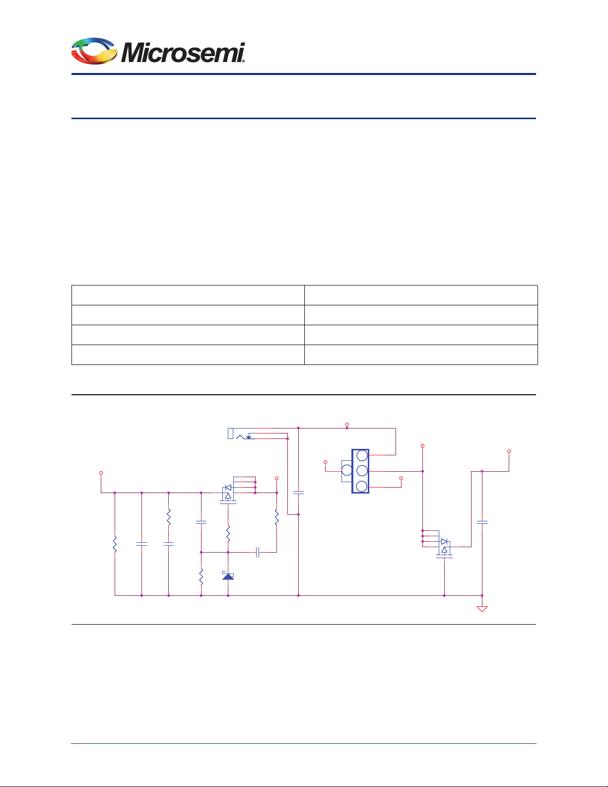
3 – Power
The IGLOO PLUS development board is powered through an external voltage power brick or USB. The
board does not switch seamlessly between the power brick and USB, so the 4-pin header and jumper
must be used to select the desired power source. In the USB option, the in-rush current meets the USB
specifications (see Figure 3-1). The power brick option is provided in applications when 100% of the total
I/Os are utilized and USB power is insufficient. A green LED next to the USB jack is ON whenever the
USB power supply is connected.
The development board has an input of a 5 V supply from the power brick or USB. Protection diodes are
used to protect against negative voltage. Three voltage rails are provided, as shown in Ta bl e 3 - 1 (3.3 V,
2.5 V, and 1.5 V).
The regulator can be switched between the 1.5 V and 1.2 V rail because the FPGA core functions at
1.2 V, but is programmed at 1.5 V.
Table 3-1 • Power Regulator Current Ratings
Regulator Current Rating
3.3 V 2A
2.5V 1A
1.5 V / 1.2 V 500 mA
Manufacturer = CUI INC
Manufacturer = CUI INC
Mfg P/N = PJ-002AH
Mfg P/N = PJ-002AH
CONN JACK PWR
CONN JACK PWR
5V BRICK
5V_USB
R6
R6
22 OHM
22 OHM
R0402
R0402
R65
R65
C6
0.1uFC60.1uF
C7
0.1uFC70.1uF
R8
R8
220K
220K
R0402
R0402
10K
10K
Figure 3-1 • USB Active Inrush Limiter
Q2
Q2
4
C8
0.1uFC80.1uF
ACTIVE INRUSH LIMITER
J10
J10
Si3407DV
Si3407DV
3
R5
R5
22 OHM
22 OHM
R0402
R0402
D10
D10
1 3
BAT54
BAT54
BAT
WALL
2
J9
J9
4PIN_HEADER
4PIN_HEADER
5V_SOURCE
3
4
VUSB
1
Q1 ONLY
INSTALLED ON
FACTORY DEMO
Q1
Q1
6
5
2
1 4
SI3407DV
SI3407DV
3
5V
C3
0.1uFC30.1uF
1
3
2
VUSB
6
5
2
1
R4
R4
2.7K
2.7K
R0402
R0402
C4
C4
0.027UF
0.027UF
C0402
C0402
2
C5
0.1uFC50.1uF
Revision 1 23
Page 24

Power
Power Modes
In addition to the board, the IGLOO PLUS FPGA offers power advantages. Some key power advantages
of the IGLOO PLUS FPGAs are as follows:
• Flash*Freeze technology enables easy entry and exit from the static Low-power mode, where
IGLOO consumes as little as 5 µW while retaining the contents of the system memory and data
registers.
• Sleep (and shutdown) mode allows the IGLOO PLUS FPGA core power supply (or all power
supplies) to be powered down when functionally is not required, while the rest of the system
remains powered.
• The user low static ICC macro (ULSICC) reduces IGLOO PLUS FPGA dynamic and static power
consumption. The ULSICC macro, when enabled, disables the FlashROM, reducing the overall
power of the device.
Table 3-2 gives a summary of the power modes available with IGLOO PLUS devices in general and is
extracted from the “Flash*Freeze Technology and Low Power Modes” chapter of the IGLOO PLUS
FPGA Fabric User’s Guide.
Table 3-2 • Power Modes
ULSICC
Mode VCC VCCI Core Clocks
Active On On On On N/A Initiate clock None –
Static Idle On On On Off N/A Stop clock Initiate clock External
Flash*Freeze
Type 1
Flash*Freeze
Type 2
Sleep On Off Off Off N/A Shut down
Shutdown Off Off Off Off N/A Shut down
a. External clocks can be left toggling while the device is in Flash*Freeze mode. Clocks generated by the embedded PLL
will be turned off automatically.
On On On On* N/A Assert FF pin Deassert FF
On On On On
a
Macro
Used to enter
Flash*Freeze
mode
To E n ter
Mode
Assert FF pin
and LSICC
VCC
VCCand
VCCI
supplies
To R e s ume
Operation Trigger
External
pin
Deassert FF
pin
Turn on
supply
VCC
Turn on
VCC and
VCCI
supplies
External
External
External
24 Revision 1
Page 25

Battery
BAT
EXTERNAL
BATTERY
SOURCE
1
2
J7
BATTERY
1x2_100MIL
J7
BATTERY
1x2_100MIL
In addition to the power brick and USB, this board provides the option to power-up via battery. No battery
casing is provided on the board. Jumpers should be set correctly to select the option of either powering
through a wall/USB or through batteries hooked up externally. To provide a 3 V input source from battery,
two AA Alkaline cells may be used. A 2-pin jumper for VBAT and GND must be provided to the input of
the main regulator to give the option of either powering through a wall/USB or powering through batteries
hooked up externally.
Figure 3-2 • Battery Header and Power Input Schematics
Potentiometer and Voltage-Sweep
A potentiometer is located on the left hand side of the board to provide the voltage-sweep function to
sweep VCC (Figure 3-3). One primary function of the potentiometer is to show battery operation on the
IGLOO PLUS device and how the FPGA can operate successfully even if V
voltage. You can measure the lowest possible V
you should also monitor the VCC via current measurement headers (Figure 3-4 on page 26) to make sure
it does not go beyond the specified value.
CC
IGLOO PLUS Starter Kit User’s Guide
experiences a drop in
CC
for battery operations. When using the potentiometer,
3.3 V
2.5 V
-Sweep
V
CCI
1.5 V
-Sweep
V
CCI
V
-Sweep
CCI
Figure 3-3 • Current Measurement Headers
3.3 V
3.3 V
3.3 V
3.3 V
Current
Measurement
IGLOO PLUS
VCCI_0
VCCI_1
VCCI_2
VCCI_3
V
CC
V
JTAG
V
PUMP
Revision 1 25
Page 26

Power
C351uF C351uF
Figure 3-4 • Schematic for Potentiometer
Current Measurement
Once the IGLOO PLUS evaluation board is powered up, you can evaluate power consumption using the
current measurement four-pin headers on the board (Figure 3-5). Current measurement can be made
without powering down the board.
RV1
RV1
5K pot
5K pot
1V5_1V2
13
2
VCC_SWEEP
Set the multimeter to measure current and attach the probes to pins 1 and 4
when the board is in normal operation.
Figure 3-5 • Current Measurement 4-Pin Headers
Four-pin headers are used for current measurement of the rails shown in Figure 3-6 on page 27. All
banks are separated and two of the banks have an option to power-up though a 3.3 V or 2.5 V source, as
shown in Figure 3-7 on page 27. Voltage sources can be selected using jumpers or can be selected to
sweep between 1.2 V and 1.5 V using the potentiometer on the development board.
Remove jumper from pins 2-3 for current measurement without
powering down.
26 Revision 1
Page 27

Current
VCORE
VCCI_1
VCCI_0
VCCI_2
VCCI_3
1V5_1V2
V3P3
V3P3
V3P3
2V5
1V5_1V2
V3P3
2V5
1V5_1V2
VCC_SWEEP
VCC_SWEEP
VCC_SWEEP
1
2
3
4
J12
HDR_4PIN
J12
HDR_4PIN
1
2
3
4
J8
HDR_4PIN
J8
HDR_4PIN
1
2
3
J18
HDR_3PIN
J18
HDR_3PIN
1
2
3
J14
HDR_3PIN
J14
HDR_3PIN
1
2
3
4
J16
4PIN_HEADER
J16
4PIN_HEADER
1
2
3
J11
HDR_3PIN
J11
HDR_3PIN
1
2
3
4
J17
HDR_4PIN
J17
HDR_4PIN
1
2
3
4
J19
4PIN_HEADER
J19
4PIN_HEADER
1
2
3
4
J13
HDR_4PIN
J13
HDR_4PIN
1
2
3
4
J6
HDR_4PIN
J6
HDR_4PIN
Measurement
IGLOO PLUS Starter Kit User’s Guide
IGLOO PLUS
3.3 V
3.3 V
3.3 V or 2.5 V
3.3 V or 2.5 V
1.5 V
3.3 V
3.3 V
Figure 3-6 • Current Measurement Headers for Power Rails
The schematic in Figure 3-7 shows the options for power-up.
VCCI_0
VCCI_1
VCCI_2
VCCI_3
V
CC
V
JTAG
V
PUMP
Figure 3-7 • Power-Up Options
Revision 1 27
Page 28

Page 29

4 – Operation of Board Components
This chapter describes operation of the IGLOO PLUS evaluation board.
Clock Oscillator
One 20 MHz clock oscillator with 50 PPM is provided on the board. This clock oscillator is connected to
the FPGA to provide a system or reference clock. The PLL can be configured and instantiated in the
FPGA to generate a wide range of clock frequencies.
Reference
For more information, refer to the IGLOO PLUS Starter Kit website page:
www.microsemi.com/soc/products/hardware/devkits_boards/iglooplus_starter.aspx.
Schematic
Figure 4-1 shows the schematic for the clock oscillator.
V3P3
U10
C390.1uF C390.1uF
U10
4
VDD
R43
R43
10K
10K
1
OUT_EN
OSCILLATOR
OSCILLATOR
Mfg P/N = SIT8002AC-43-33E
Mfg P/N = SIT8002AC-43-33E
Manufacturer = SI TIME
Manufacturer = SI TIME
OUTPUT
GND
3
2
R6422R64
22
OSC_CLK [4]
Figure 4-1 • Clock Oscillator Schematic
Reset
An RC type push-button reset switch to the FPGA is provided on-board. The Schmitt Trigger chip (U13),
however, is NOT populated. An on-board Schmitt Trigger chip is not required because Schmitt Trigger is
one of the many advanced I/O features of the IGLOO PLUS FPGA family. To improve noise immunity,
ensure that the Schmitt Trigger option for this reset input pin is enabled in the FPGA design. If the IGLOO
PLUS FPGA is swapped out with a device that does not have the advance Schmitt Trigger I/O feature,
the Schmitt Trigger chip (U13) should be populated.
Revision 1 29
Page 30

Operation of Board Components
V3P3
V3P3
PBRESET_N [4]
Mfr P/N :KSC403J 50SH LFG
Mfr:ITT INDUSTRIES
Mfr P/N :DS1818R-20+T&R
Mfr: Dallas
RST
C65
0.1uF
C65
0.1uF
VCC
2
GND
3
RST
1
U13
DNP
U13
DNP
R630R63
0
12
34
SW7
KSC403J
SW7
KSC403J
R62
10K
R62
10K
C660.1uF C660.1uF
Schematic
Figure 4-2 shows the schematic for reset.
Figure 4-2 • Reset Schematic
Flash*Freeze Mode
The IGLOO PLUS device has an ultra-low-power static mode, called Flash*Freeze mode, which retains
all SRAM and register information and can still quickly return to normal operation (Figure 4-1).
Flash*Freeze technology enables the user to quickly (within 1 µs) enter and exit Flash*Freeze mode by
activating the Flash*Freeze pin while all power supplies are kept at their original values. I/Os, global I/Os,
and clocks can still be driven and can be toggling without impact on power consumption, and the device
retains all core registers, SRAM information, and I/O states. I/Os can be individually configured to either
hold their previous state or can be tristated during Flash*Freeze mode.
Flash*Freeze
Mode Control
IGLOO PLUS
FPGA
Flash*Freeze Pin
Figure 4-3 • Flash*Freeze Mode Control
There are two ways to use Flash*Freeze mode. In Flash*Freeze type 1, entering and exiting the mode is
exclusively controlled by the assertion and deassertion of the FF pin. This enables an external processor
or human interface device to directly control Flash*Freeze mode. In Flash*Freeze mode type 2, entering
and exiting the mode is controlled by both the FF pin AND user-defined logic. Flash*Freeze management
IP can be used in type 2 mode for clock and data management while entering and exiting Flash*Freeze
mode.
For more information and detailed usage of Flash*Freeze modes, refer to the “Microsemi’s Flash*Freeze
Technology and Low Power Modes” chapter of the IGLOO PLUS FPGA Fabric User’s Guide.
30 Revision 1
Page 31

IGLOO PLUS Starter Kit User’s Guide
M
Normal
Normal
F
Flash*Freeze Types
Type 1: Controlled by dedicated Flash*Freeze Pin.
Type 2: Controlled by dedicated Flash*Freeze Pin and Internal Logic.
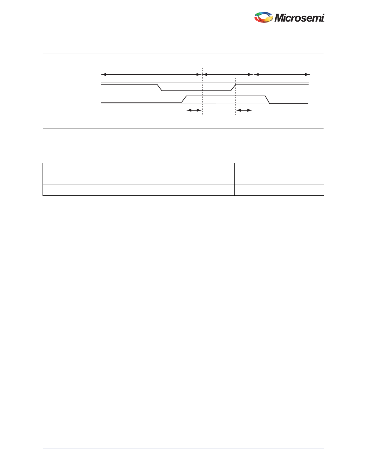
Flash*Freeze Type 1: Controlled by Dedicated Flash*Freeze Pin
Flash*Freeze type 1 is intended for systems where either the device is reset upon exiting Flash*Freeze
mode, or data and clock are managed externally. The device enters Flash*Freeze mode 1 µs after the
dedicated FF pin is asserted (active low), and returns to normal operation when the FF pin is deasserted
(high). In this mode, FF pin assertion or deassertion is the only condition that determines entering or
exiting Flash*Freeze mode (Figure 4-4). An INBUF_FF I/O buffer macro must be used to identify the
Flash*Freeze input in your design.
IGLOO , IGLOO PLUS, IGLOO nano,
ProASIC3L, or RT ProASIC3 Device
Flash* Freeze
INBUF_FF
To FPGA Core or Floating
ode Control
Flash* Freeze (FF) Pin
Flash*Freeze
Signal
Flash* Freeze
Flash*Freeze
Figure 4-4 • Flash*Freeze Mode Type 1 – Controlled by the Flash*Freeze Pin
Operation
Enables Entering
Flash*Freeze M ode
AND
Mode
Technology
Flash*Freeze
Mode
1
User Design
Operation
lash*Freeze Pin
t = 1 µs t = 1 µs
Figure 4-5 • Flash*Freeze Mode Type 1 – Timing Diagram
Revision 1 31
Page 32

Operation of Board Components
INBUF_FF
Auto-Connected to IP
ULSICC Macro
Flash*Freeze
Management IP
User Design
IGLOO, IGLOO PLUS, IGLOO nano,
ProASIC3L, or RT ProASIC3 Device
Flash*Freeze
Mode
Enables Entering
Flash*Freeze Mode
Flash*Freeze
Signal
Flash*Freeze
Technology
Flash*Freeze (FF) Pin
AND
Connect to Top-Level Port
Flash*Freeze Type 2: Controlled by Dedicated Flash*Freeze Pin and
Internal Logic
The device can be made to enter Flash*Freeze mode by activating the FF pin together with the
Flash*Freeze management IP core or user-defined control logic (Figure 4-6) within the FPGA core. This
method enables the design to perform important activities before allowing the device to enter
Flash*Freeze mode, such as transitioning into a safe state, completing the processing of a critical event.
Designers are encouraged to take advantage of the Flash*Freeze Management IP of Microsemi to
handle clean entry and exit of Flash*Freeze mode. The device will only enter Flash*Freeze mode when
the Flash*Freeze pin is asserted (active low) and the User Low Static ICC (ULSICC) macro input signal,
called the LSICC signal, is asserted (high). One condition is not sufficient to enter Flash*Freeze mode
type 2; both the FF pin and LSICC signal must be asserted.
Figure 4-7 shows the timing diagram for entering and exiting Flash*Freeze mode type 2. After exiting
Flash*Freeze mode type 2 by deasserting the Flash*Freeze pin, the LSICC signal must be deasserted by
the user design. This will prevent entering Flash*Freeze mode by asserting the Flash*Freeze pin only.
Refer to Figure 4-1 on page 29 for Flash*Freeze (FF) pin and LSICC signal assertion and deassertion
values.
Figure 4-6 • Flash*Freeze Mode Type 2 – Controlled by Flash*Freeze Pin and Internal Logic (LSICC signal)
32 Revision 1
Page 33
IGLOO PLUS Starter Kit User’s Guide
Normal
Normal
F
Operation
lash*Freeze Pin
LSICC Signal
t = 1 µs t = 1 µs
Figure 4-7 • Flash*Freeze Mode Type 1 and Type 2 – Signal Assertion and Deassertion Values
Table 4-1 • Flash*Freeze Mode Type 1 and Type 2 – Signal Assertion and Deassertion Values
Signal Assertion Value Deassertion Value
Flash*Freeze (FF) pin Low High
LSICC signal High Low
Note:
1. The Flash*Freeze (FF) pin is an active-Low signal, and LSICC is an active-High signal.
2. The LSICC signal is used only in Flash*Freeze mode type 2.
Flash*Freeze
Mode
Operation
IGLOO PLUS I/O State in Flash*Freeze Mode
In IGLOO PLUS devices, users have multiple options in how to configure I/Os during Flash*Freeze
mode:
1. Hold the previous state.
2. Set I/O pad to weak pull-up or pull-down.
3. Tristate I/O pads.
The I/O configuration must be configured by the user in the I/O Attribute Editor or in a PDC constraint file,
and can be done on a pin-by-pin basis. The output hold feature will hold the output in the last registered
state, using the I/O pad weak pull-up or pull-down resistor when the FF pin is asserted. When inputs are
configured with the hold feature enabled, the FPGA core side of the input will hold the last valid state of
the input pad before the device entered Flash*Freeze mode. The input pad can be driven to any value,
configured as tristate, or configured with the weak pull-up or pull-down I/O pad feature during
Flash*Freeze mode, without affecting the hold state. If the weak pull-up or pull-down feature is used
without the output hold feature, the input and output pads will maintain the configured weak pull-up or
pull-down status during Flash*Freeze mode and normal operation. If a fixed weak pull-up or pull-down is
defined on an output buffer or as bidirectional in output mode, and a hold state is also defined for the
same pin, the pin will be configured in hold state mode during Flash*Freeze mode. During normal
operation, the pin will be configured with the predefined weak pull-up or pull-down. Any I/Os that do not
use the hold state or I/O pad weak pull-up or pull-down features will be tristated during Flash*Freeze
mode and the FPGA core will be driven high by inputs. Inputs that are tristated during Flash*Freeze
mode may be left floating without any reliability concern or impact to power consumption.
Revision 1 33
Page 34

Operation of Board Components
Table 4-2 shows the I/O pad state based on the configuration and buffer type.
Table 4-2 • IGLOO PLUS Flash*Freeze Mode (type 1 and type 2)—I/O Pad State
Buffer Type Hold State
I/O Pad
Weak Pull-Up/-Down
I/O Pad State in Flash*Freeze
Mode
Input Enabled Enabled Weak pull-up/pull-down
Disabled Enabled Weak pull-up/pull-down
Enabled Disabled Tristate
Disabled Disabled Tristate
1
2
Output Enabled “Don't care” Weak pull to hold state
Disabled Enabled Weak pull-up/pull-down
Disabled Disabled Tristate
Bidirectional /
Tristate Buffer
E = 0
(input/tristate)
Enabled Enabled Weak pull-up/pull-down
Disabled Enabled Weak pull-up/pull-down
Enabled Disabled Tristate
Disabled Disabled Tristate
1
2
E = 1 (output) Enabled “Don't care” Weak pull to hold state
Disabled Enabled Weak pull-up/pull-down
Disabled Disabled Tristate
1
2
1
2
3
Note:
1) Internal core logic driven by this input buffer will be set to the value this I/O had when entering Flash*Freeze
mode.
2) Internal core logic driven by this input buffer will be tied High as long as the device is in Flash*Freeze mode.
3) For bidirectional buffers: Internal core logic driven by the input portion of the bidirectional buffer will be set to
the hold state.
34 Revision 1
Page 35

Flash*Freeze Switch
V3P3
V3P3
IGLOO_FF [4]
Mfr P/N :AYZ0102AGRL
Mfr: ITT INDUSTRIES
R61
10K
R61
10K
2
1
3
SW8
AYZ0102AGRL
SW8
AYZ0102AGRL
+
C6410uF+C6410uF
C630.1uF C630.1uF
R520R52
0
C61
0.1uF
C61
0.1uF
NC
1
A
2
GND
3
VCC
5
Y
4
U12
DNP
Mfg P/N = SN74AUP1G17DCKR
Manufacturer = TI
U12
DNP
Mfg P/N = SN74AUP1G17DCKR
Manufacturer = TI
+
C622.2uF+C622.2uF
An F*F switch is provided on the board for designs that utilize the Flash*Freeze technology. Setting the
F*F switch to FF_ON will enable the Flash*Freeze mode of the IGLOO PLUS device. Since the Schmitt
Trigger chip (U12) is NOT populated on-board for the F*F switch, the Schmitt Trigger feature should be
enabled in the FPGA design for the Flash*Freeze input to enhance noise immunity (Figure 4-8). The
Schmitt Trigger is an advanced I/O feature of the IGLOO PLUS FPGA family. If the IGLOO PLUS FPGA
is swapped out with a device that does not have the advanced Schmitt Trigger I/O feature, the Schmitt
Trigger chip (U12) should be populated
Figure 4-8 • Flash*Freeze Schematic, Schmitt Triggered
.
IGLOO PLUS Starter Kit User’s Guide
Some features on this board are included to demonstrate the Flash*Freeze variants of the IGLOO PLUS
FPGA. I/Os can be individually configured to either hold their previous state or be tristated during
Flash*Freeze mode. Alternatively, they can be set to a certain state (high or low) using weak pull-up or
pull-down I/O attribute configurations. These Flash*Freeze variants can be demonstrated by configuring
the I/Os in Designer and using switches as inputs to control the FET LEDs. Refer to the demo design,
which provides additional details on demonstrating these Flash*Freeze variants ("IGLOO PLUS Board
Demo" on page 51).
Flash*Freeze Variant Dip Switch
Two regular DIP switches are located on the board, next to the FET LEDs (Figure 4-9). The DIP switches
can be programmed to help debug or demonstrate the Flash*Freeze variants. Refer to the demo design
that demonstrates the Flash*Freeze variants with these switches.
R20
R20
10K
R22
R22
R19
R19
DNL
DNL
10K
10K
10K
SW5
SW5
1
2
76SB02ST
R21
R21
DNL
DNL
LO T67K-L1M2-24-Z_DNL
LO T67K-L1M2-24-Z_DNL
D11
D11
LO T67K-L1M2-24-Z_DNL
LO T67K-L1M2-24-Z_DNL
D12
D12
76SB02ST
3
4
3V3_SWITCH1
[4]
3V3_SWITCH2
[4]
3V3_SWITCH1
[4]
3V3_SWITCH2
[4]
Figure 4-9 • Two I/Os Controlled through DIP Switch Toggling High or Low
Revision 1 35
Page 36

Operation of Board Components
Flash*Freeze Variant FET LEDs
These FET LEDs can be used for debugging, such as for viewing the state of I/Os in Flash*Freeze mode.
These LEDs can be activated (ON) before entering Flash*Freeze mode, and have the ability to remain
activated (ON) in Flash*Freeze mode. In low-power or Flash*Freeze mode, the FET LEDs can continue
to function normally. There is one N-Type FET LED and two P-Type FET LEDs on the board
(Figure 4-10). Refer to "Demo 4 – Flash*Freeze Variant: Configuration Settings of Demo Design" on
page 52, which will help demonstrate the Flash*Freeze variants.
Q4
Q4
P TYPE FET
Q6
V3P3 V3P3
Q6
R49
R49
1.5K
1.5K
MOSFET_PTYPE
MOSFET_PTYPE
LO T67K-L1M2-24-Z
LO T67K-L1M2-24-Z
Mfg P/N = FDV304P
Mfg P/N = FDV304P
Manufacturer = FairChild
Manufacturer = FairChild
D13
D13
2
D
D
3
S
S
R51
G
G
1
FET_P1 [4] FET_P2 [4]
V3P3
R50
R50
1.5K
1.5K
LO T67K-L1M2-24-Z
LO T67K-L1M2-24-Z
D15
D15
N TYPE FET
MOSFET_NTYPE
MOSFET_NTYPE
Mfg P/N = FDV301N
Mfg P/N = FDV301N
Manufacturer = FairChild
Manufacturer = FairChild
FET_N[4]
Q5
Q5
D
D
2 3
R51
1.5K
1.5K
LO T67K-L1M2-24-Z
LO T67K-L1M2-24-Z
D14
D14
S
S
G
G
1
2
D
D
MOSFET_PTYPE
MOSFET_PTYPE
Mfg P/N = FDV304P
Mfg P/N = FDV304P
Manufacturer = FairChild
Manufacturer = FairChild
3
S
S
G
G
1
Figure 4-10 • FET LEDs for Debugging
36 Revision 1
Page 37

Push-Button Switches
V3P3
SWITCH1 [4]
SWITCH2 [4]
SWITCH1 [4]
SWITCH2 [4]
SWITCH3 [4] SWITCH4 [4]
SWITCH3 [4]
SWITCH4 [4]
Mfr P/N :KSC403J 50SH LFG
Mfr:ITT INDUSTRIES
Mfr P/N :KSC403J 50SH LFG
Mfr:ITT INDUSTRIES
Mfr P/N :KSC403J 50SH LFG
Mfr:ITT INDUSTRIES
Mfr P/N :KSC403J 50SH LFG
Mfr:ITT INDUSTRIES
R32
10K
R32
10K
1 2
3
4
SW1
KSC403J
SW1
KSC403J
R33
10K
R33
10K
1 2
3
4
SW4
KSC403J
SW4
KSC403J
1
2
3
4
SW3
KSC403J
SW3
KSC403J
1 2
3 4
SW2
KSC403J
SW2
KSC403J
R34
10K
R34
10K
R23
10K
R23
10K
Four active low push-button switches are provided on the board for debug purposes. You can remove the
corresponding jumpers to detach or isolate any of the four push-button test switches from the FPGA I/O.
Schematics are shown in Figure 4-11 and Figure 4-12.
IGLOO PLUS Starter Kit User’s Guide
Figure 4-11 • Push-Button Switches Schematic
J36
J36
HDR1X2
HDR1X2
J38
J38
HDR1X2
HDR1X2
1
HDR1X2
HDR1X2
1
2
J23
J23
1
2
2
J37
J37
HDR1X2
HDR1X2
1
2
J39
J39
HDR1X2
HDR1X2
1
2
SWITCH1 [6]
SWITCH2 [6]
SWITCH3 [6]
SWITCH4 [6]
3V3_SWITCH1 [8]
Figure 4-12 • Jumper Header Schematic for Push-Button Switches
Revision 1 37
Page 38

Operation of Board Components
V3P3
D_SWITCH1 [4]
D_SWITCH2 [4]
D_SWITCH3 [4]
D_SWITCH4 [4]
D_SWITCH5 [4]
D_SWITCH6 [4]
D_SWITCH7 [4]
D_SWITCH8 [4]
D_SWITCH1 [4]
D_SWITCH2 [4]
D_SWITCH3 [4]
D_SWITCH4 [4]
D_SWITCH5 [4]
D_SWITCH6 [4]
D_SWITCH7 [4]
D_SWITCH8 [4]
R54 4.7KR54 4.7K
R56 4.7KR56 4.7K
R53 4.7KR53 4.7K
R57 4.7KR57 4.7K
R55 4.7KR55 4.7K
R60 4.7KR60 4.7K
R58 4.7KR58 4.7K
1
2
3
4
5
6
7
8
16
15
14
13
12
11
10
9
DSW5
DIP_SWITCH
Manufacturer = GRAYHILL Inc
Mfg P/N = 76SB08ST
DSW5
DIP_SWITCH
Manufacturer = GRAYHILL Inc
Mfg P/N = 76SB08ST
R59 4.7KR59 4.7K
.DIP Switches
A DIP switch pack (8 switches) is provided on the board (Figure 4-13 and Figure 4-14). You can remove
the corresponding jumpers to detach or isolate any of the eight DIP Switches from the FPGA I/Os..
Figure 4-13 • DIP Switches Schematic
J29
J29
HDR1X2
HDR1X2
1
Figure 4-14 • Jumper Header Schematic for DIP Switches
38 Revision 1
2
J31
J31
HDR1X2
HDR1X2
2
J33
J33
HDR1X2
HDR1X2
2
J35
J35
HDR1X2
HDR1X2
2
1
1
1
J28
J28
HDR1X2
HDR1X2
2
J30
J30
HDR1X2
HDR1X2
2
J32
J32
HDR1X2
HDR1X2
2
J34
J34
HDR1X2
HDR1X2
2
1
1
1
1
D_SWITCH1 [6]
D_SWITCH2 [6]
D_SWITCH3 [6]
D_SWITCH4 [6]
D_SWITCH5 [6]
D_SWITCH6 [6]
D_SWITCH7 [6]
D_SWITCH8 [6]
Page 39

User LEDs
Eight active low debug LEDs are provided on the board (Figure 4-15 and Figure 4-16). You can remove
the corresponding jumpers from the 8 × 2 headers to detach or isolate any of the eight LEDs from the
FPGA I/Os.
IGLOO PLUS Starter Kit User’s Guide
V3P3
R24
LED1[4]
LED2
[4]
LED3
[4]
LED4[4]
R24
R25
R25
R26
R26
R27
R27
1.5K
1.5K
1.5K
1.5K
1.5K
1.5K
1.5K
1.5K
D1
D1
LO T67K-L1M2-24-Z
LO T67K-L1M2-24-Z
D2
D2
LO T67K-L1M2-24-Z
LO T67K-L1M2-24-Z
D3
D3
LO T67K-L1M2-24-Z
LO T67K-L1M2-24-Z
D4
D4
LO T67K-L1M2-24-Z
LO T67K-L1M2-24-Z
Mfr P/N :LO T67K-L1M2-24-Z
Mfr: Osram Opto Semiconductors Inc
V3P3
[4]
LED5
LED6[4]
LED7
[4]
LED8[4]
Figure 4-15 • User LEDs Schematic
J29
J29
HDR1X2
HDR1X2
2
J31
J31
HDR1X2
HDR1X2
2
J33
J33
HDR1X2
HDR1X2
2
J35
J35
HDR1X2
HDR1X2
2
R28
R28
1.5K
1.5K
R29
R29
1.5K
1.5K
R30
R30
1.5K
1.5K
R31
R31
1.5K
1.5K
J28
J28
HDR1X2
HDR1X2
1
2
J30
J30
HDR1X2
HDR1X2
1
1
2
J32
J32
HDR1X2
HDR1X2
1
1
2
J34
J34
HDR1X2
HDR1X2
1
1
2
1
D5
D5
LO T67K-L1M2-24-Z
LO T67K-L1M2-24-Z
D6
D6
LO T67K-L1M2-24-Z
LO T67K-L1M2-24-Z
D7
D7
LO T67K-L1M2-24-Z
LO T67K-L1M2-24-Z
D8
D8
LO T67K-L1M2-24-Z
LO T67K-L1M2-24-Z
D_SWITCH1 [6]
D_SWITCH2 [6]
D_SWITCH3 [6]
D_SWITCH4 [6]
D_SWITCH5 [6]
D_SWITCH6 [6]
D_SWITCH7 [6]
D_SWITCH8 [6]
Figure 4-16 • Jumper Header Schematic for User LEDs
Revision 1 39
Page 40

Operation of Board Components
GND
GND
IGLOO PL US
IO_B0
IO_B1
IO_B2
IO_B3
100 mils × N
(N = 1, 2, 3, 4, .. .)
TP272TPTP272
TP
TP57TPTP57
TP
TP263TPTP263
TP
TP194TPTP194
TP
TP306TPTP306
TP
TP313TPTP313
TP
TP51TPTP51
TP
TP257TPTP257
TP
TP324TPTP324
TP
TP188TPTP188
TP
TP300TPTP300
TP
TP283TPTP283
TP
TP318TPTP318
TP
TP294TPTP294
TP
TP277TPTP277
TP
TP62TPTP62
TP
TP268TPTP268
TP
TP327TPTP327
TP
TP251TPTP251
TP
TP199TPTP199
TP
TP291TPTP291
TP
TP328TPTP328
TP
TP271TPTP271
TP
TP56TPTP56
TP
TP262TPTP262
TP
TP250TPTP250
TP
TP193TPTP193
TP
TP305TPTP305
TP
TP312TPTP312
TP
TP67TPTP67
TP
TP256TPTP256
TP
TP323TPTP323
TP
TP187TPTP187
TP
TP299TPTP299
TP
TP282TPTP282
TP
TP198TPTP198
TP
TP317TPTP317
TP
TP293TPTP293
TP
TP276TPTP276
TP
TP61TPTP61
TP
TP267TPTP267
TP
TP304TPTP304
TP
TP311TPTP311
TP
TP270TPTP270
TP
TP55TPTP55
TP
TP261TPTP261
TP
TP280TPTP280
TP
TP192TPTP192
TP
TP281TPTP281
TP
TP66TPTP66
TP
TP63TPTP63
TP
TP255TPTP255
TP
TP322TPTP322
TP
TP186TPTP186
TP
TP298TPTP298
TP
TP197TPTP197
TP
TP316TPTP316
TP
TP292TPTP292
TP
TP275TPTP275
TP
TP60TPTP60
TP
TP266TPTP266
TP
TP191TPTP191
TP
TP303TPTP303
TP
TP310TPTP310
TP
TP286TPTP286
TP
TP54TPTP54
TP
TP260TPTP260
TP
TP279TPTP279
TP
TP297TPTP297
TP
TP65TPTP65
TP
TP254TPTP254
TP
TP321TPTP321
TP
TP307TPTP307
TP
TP185TPTP185
TP
TP59TPTP59
TP
TP265TPTP265
TP
TP196TPTP196
TP
TP315TPTP315
TP
TP274TPTP274
TP
TP326TPTP326
TP
TP190TPTP190
TP
TP302TPTP302
TP
TP309TPTP309
TP
TP285TPTP285
TP
TP53TPTP53
TP
TP259TPTP259
TP
TP184TPTP184
TP
TP296TPTP296
TP
TP64TPTP64
TP
TP202TPTP202
TP
TP253TPTP253
TP
TP320TPTP320
TP
TP165TPTP165
TP
TP273TPTP273
TP
TP58TPTP58
TP
TP264TPTP264
TP
TP195TPTP195
TP
TP314TPTP314
TP
TP258TPTP258
TP
TP325TPTP325
TP
TP189TPTP189
TP
TP301TPTP301
TP
TP290TPTP290
TP
TP308TPTP308
TP
TP284TPTP284
TP
TP52TPTP52
TP
TP295TPTP295
TP
TP278TPTP278
TP
TP200TPTP200
TP
TP269TPTP269
TP
TP201TPTP201
TP
TP252TPTP252
TP
TP319TPTP319
TP
V3P3
2V5
1V5_1V2
TP13TPTP13
TP
TP1TPTP1
TP
TP12TPTP12
TP
TP3TPTP3
TP
TP11TPTP11
TP
TP8TPTP8
TP
TP5TPTP5
TP
TP6TPTP6
TP
TP9TPTP9
TP
I/O Test Pins
All IGLOO PLUS FPGA I/Os are available on headers located on the top and bottom of the device
(Figure 4-17 and Figure 4-18). These test pins are multiples of 100 mils apart, so developers can easily
attach headers and place an extension card on top with an off-the-shelf breadboard for a low-cost
solution for integration. In order to use I/Os assigned to the LEDs, DIP Switches, and push-button
switches, the 2-pin jumper on their path must be removed first to disconnect the assignment.
Figure 4-17 • I/O Test Pins
Figure 4-18 • I/O Test Pins Schematic
40 Revision 1
Page 41

OLED
VP_10V
V3P3
V3P3
PACER_D0 [4]
PACER_RES# [4]
PACER_D2 [4]
SCL
SDA
Mfr P/N :PMO13701
Mfr: PACER
VCC
30
VCOMH
29
IREF
28
VDD
11
BS1
12
BS2
13
NC1
1
NC2
8
NC3
9
NC4
10
NC5
14
NC6
31
VSS
2
D7
27
D6
26
D5
25
D4
24
D3
23
D2
22
D1
21
D0
20
TEST5
3
TEST4
4
TEST3
5
TEST2
6
TEST1
7
RD#
19
WR#
18
D/C#
17
RES#
16
CS#
15
U3
PMO13701
U3
PMO13701
C20
0.01uF
C20
0.01uF
R36
10K
R36
10K
+
C21
4.7uF 16V
+
C21
4.7uF 16V
R372MR37
2M
C19
1uF
C19
1uF
R35
10K
R35
10K
IGLOO PLUS Starter Kit User’s Guide
A 96 × 16 pixel low-power blue organic light emitting diode (OLED) is available on the board above the
IGLOO PLUS FPGA (Figure 4-19). The OLED features a serial I2C interface, and is capable of
displaying sharp images or text. The demo design included in this kit contains a roulette game that uses
the OLED for display and the push-button switch for game control.
Additional OLED info is available at the IGLOO PLUS Starter Kit website page:
www.microsemi.com/soc/products/hardware/devkits_boards/iglooplus_starter.aspx.
Figure 4-19 • OLED Display Schematic
Revision 1 41
Page 42

Operation of Board Components
VUSB
V3P3
GPIOA_29
{3}
GPIOA_33
{3}
GPIOA_31
{3}
GPIOA_35
{3}
GPIOA_34 {3}
GPIOA_36 {3}
GPIOA_26 {3}
GPIOA_28 {3}
GPIOA_30 {3}
GPIOA_32 {3}
GPIOA_10 {3}
GPIOA_8 {3}
GPIOA_6 {3}
GPIOA_12 {3}
GPIOA_16 {3}
GPIOA_18 {3}
GPIOA_20 {3}
GPIOA_24 {3}
GPIOA_22 {3}
GPIOA_2 {3}
GPIOA_4 {3}
GPIOA_9
{3}
GPIOA_13{3}
GPIOA_15{3}
GPIOA_17{3}
GPIOA_19{3}
GPIOA_21{3}
GPIOA_23
{3}
GPIOA_7{3}
GPIOA_5{3}
GPIOA_1{3}
GPIOA_3{3}
GPIOA_25
{3}
GPIOA_27{3}
20x2 Edge Fingers
Pin No:15 & 16 Should be NC For Matting Connector Polarised Pins
Matting Conn P/N: MEC1-120-02-F-S-EM2
Mfr : Samtec
2
4
6
8
10
12
14
18
20
24
22
26
28
30
32
34
36
38
40
39
37
35
33
31
29
27
25
23
21
19
17
13
11
9
7
5
3
1
J48
HDR_20x2
J48
HDR_20x2
Interface Connector
A standard interface connector on the board can be used to connect additional daughter cards, some of
which are developed by partners and third party vendors (Figure 4-20). The interface possibilities are
numerous, such as flash and SRAM memory interfaces, keyboard interfaces for embedded applications,
LCD interfaces, and motor control interfaces. GPIOA_1, GPIOA_2, GPIOA_4, and GPIOA_31 pins can
be used for critical signals, such as clock and reset, because proper series termination has been
provided on these signal lines.
Figure 4-20 • Interface Connector Schematic
USB-to-UART Interface
Included on the starter kit board is a USB-to-UART interface with ESD protection. This interface includes
an integrated USB-to-UART bridge controller to provide a standard UART connection with the IGLOO
PLUS FPGA. Any standard UART controller can be implemented in the IGLOO PLUS FPGA to allow
access with this interface. In addition, the Microsemi IP catalog includes various UART controllers,
specifically CoreUART, which can be instantiated in the FPGA design with an embedded processor.
CoreUART controller supports both asynchronous and synchronous modes with configurable
parameters for various applications.
One application of the USB-to-UART interface is to allow for Hyper-terminal on a PC to communicate
with the IGLOO PLUS FPGA. HyperTerminal is a serial communications application program that can be
installed in the Windows® operating system. A basic HyperTerminal program is usually distributed with
Windows. With an USB driver properly installed, and correct COM port and communication settings
selected, you can use the HyperTerminal program to communicate with a design running in the IGLOO
PLUS FPGA device.
Information on the USB-to-UART bridge datasheet and device drivers are available at the IGLOO PLUS
Star ter Kit website page:
www.microsemi.com/soc/products/hardware/devkits_boards/iglooplus_starter.aspx.
42 Revision 1
Page 43

The USB-to-UART schematic is shown in Figure 4-21.
V3P3
V3P3
SPI_DIO[4]
SPI_DO[4]
SPI_CLK[4]
SPI_CS_N
[4]
SPI_WP_N[4]
SPI_HOLD_N[4]
SPI_DIO[4]
SPI_DO[4]
SPI_CLK
[4]
SPI_CS_N[4]
SPI_WP_N[4]
SPI_HOLD_N[4]
2 MByte
Mfr P/N : W25X16-VSSIG
Mfr: Winbond
C67
0.1uF 10V
C67
0.1uF 10V
HOLD
7
Vcc
8
CS
1
DIO
5
WP
3
GND
4
DO
2
CLK
6
SPI FLASH
16M bit
U11
W25X16
SPI FLASH
U11
W25X16
SI
1
SO
8
SCK
2
CS
4
WP
5
RESET
3
VCC
6
GND
7
SPI FLASH
16M BIT
U23
Manufacturer = Atmel
MANUFACTURER P/N = AT45BD161D-SU
SPI FLASH
16M BIT
U23
AT45DB161D-SU
Manufacturer = Atmel
MANUFACTURER P/N = AT45BD161D-SU
R47
4.87K
R47
4.87K
C50
0.1uF 10V
C50
0.1uF 10V
IGLOO PLUS Starter Kit User’s Guide
JP1
JP1
5V_USB
CON2
CON2
2
U1
USBLC6-2U1USBLC6-2
Mfr P/N :USBLC6-2SC6
Mfr: ST Micro.
1
6
IO1B
5
V
4
IO2B
J5
J5
6
GND1
7
GND2
8
GND3
9
GND4
USB_MINI_RECEP
USB_MINI_RECEP
Mfr P/N :UX60-MB-5ST
Mfr: Hirose
VBUS
PTC1
PTC1
FUSE
FUSE
Mfr P/N :MICROSMD050F-2
Mfr:Tyco
1
2
D-
3
D+
4
NC
5
GND
1
IO1A
2
G
3
IO2A
Figure 4-21 • USB-to-UART Interface Schematic
SPI Flash
One 2 Mbyte SPI flash is available on the board and can be used by CoreABC-type applications for
access of additional memory. The flash interface, serial peripheral interface bus (SPI), is a synchronous
serial data link standard that is used to access the flash memory. Some advantages of the SPI interface
are full duplex communication and higher throughput than I2C. In the schematics shown in Figure 4-22,
either the Winbond or Atmel 2 Mbyte SPI flash will be populated on-board.
Winbond and Atmel SPI flash datasheets are available at the IGLOO PLUS Starter Kit website page:
www.microsemi.com/soc/products/hardware/devkits_boards/iglooplus_starter.aspx
C18
C18
0.1uF
0.1uF
VUSB
D9
Mfr P/N :BLM31PG500SN1L
Mfr: Murata
FB1
FB1
FERRITE BEAD
FERRITE BEAD
R2
147R2147
LED_GREEND9LED_GREEN
V3P3
U2
8
VBUS
7
REGIN
6
VDD
C1
C2
10
NC1
13
0.1uFC10.1uF
NC2
14
NC3
15
NC4
16
NC5
17
NC6
5
D-
4
D+
GND3GNDNW30GNDCNTR
29
CP2102U2CP2102
1uFC21uF
DTR
RTS
CTS
DSR
RI
DCD
TXD
RXD
SUSPEND
NSUSPEND
RST
NC7
NC8
NC9
NC10
NC11
Mfr P/N :CP2102-GM
Mfr: Silicon Labs
28
R670R67
24
23
27
2
1
26
25
12
11
9
18
19
20
21
22
R1
0
10KR110K
AGL_UART_RXD [4]
AGL_UART_TXD [4]
.
Figure 4-22 • SPI Flash Schematics
Note: Either the Winbond or Atmel SPI flash will be populated on the board.
Revision 1 43
Page 44

Operation of Board Components
Low-Cost Programming Stick (LCPS)
Interface
The development board can be programmed by the low-cost programming stick (LCPS) or via a 10-pin
FP3 header (Figure 4-24). Regardless of the programming dongle used, IGLOO PLUS is programmed
the same way as IGLOO nano, ProASIC3, and Fusion FPGA devices.The LCPS is a special version for
the FlashPro3 programming circuitry that is compatible with FlashPro3 and the generic FlashPro
programming software. The LCPS, like the IGLOO PLUS board, is RoHS-compliant and is completely
lead (Pb) free. To use the LCPS with the FlashPro software, all you need to do is to select the FlashPro3
from the list of programmer types. The LCPS behaves exactly as if it were a regular encased FlashPro3
programmer, except regarding VPUMP. The LCPS does not supply VPUMP; it must be supplied by the
IGLOO PLUS board. The 12-pin female connector socket is designed to interface to the 12-pin rightangle male header on the IGLOO PLUS kit. One of the pins is a special VJTAGENB signal that goes high
when programming is taking place and returns to a low level when programming has completed. This
signal is connected to the FET on the 1.5 V regulator circuit. The IGLOO PLUS board uses this signal to
effect a change in the value of VCC from 1.2 V to 1.5 V, which is required for programming all IGLOO
PLUS devices.
You do not need to have the LCPS connected to the IGLOO PLUS board to operate it, after the FPGA
has been programmed. The LCPS must be connected to the IGLOO PLUS board only when
programming the AGLP125-CSG289.
Figure 4-23 • Low-Cost Programming Stick (LCPS)
Note:
1. The LCPS supplied with this kit is intended for use with the IGLOO PLUS Starter Kit. An LCPS
supplied for other kits, although electrically and functionally equivalent, may not connect
seamlessly with the IGLOO PLUS Starter Kit board.
2. The LCPS is not designed to supply VPUMP on its own as does the FlashPro3/4 programmer, so
the IGLOO PLUS board must supply VPUMP. Use a 5 V brick or USB port to power-up the board.
If you disconnect the VPUMP jumper, the LCPS will not work.
44 Revision 1
Page 45

IGLOO PLUS Starter Kit User’s Guide
J3
J3
Programmer
VJTAGENB[3]
TMS[5]
[5]
[5]
VJTAG
TDO
1
VJTAGENB
3
TMS
5
GND2
7
VJTAG
9
TDO
11
GND4
HEADER 6x2/SM
HEADER 6x2/SM
6X2 Right Angled Header
Mfr P/N :TSW-106-08-T-D-RA
Mfr: SAMTEC
Figure 4-24 • FPGA Programming Headers Schematic
TCK
GND3
TDI
TRSTB
VPUMP
GND5
2
4
6
8
10
12
TCK [5]
TDI [5]
TRST [5]
VPUMP [5]
Revision 1 45
Page 46

Operation of Board Components
LCPS Stackup
The LCPS is built on a four-layer PCB with the layers arranged in the following stackup:
1. Top signal layer (Figure 4-25)
2. Ground plane
3. Power plane
1. Bottom signal layer (Figure 4-26 on page 47)
Figure 4-25 • Low-Cost Programming Stick – Top Silkscreen
46 Revision 1
Page 47

IGLOO PLUS Starter Kit User’s Guide
Figure 4-26 • Low-Cost Programming Stick – Bottom Silkscreen
Revision 1 47
Page 48

Page 49

5 – Programming
Program a Design into the IGLOO PLUS Evaluation Board
1. To program a design into the IGLOO PLUS evaluation board, attach the LCPS board to the
IGLOO PLUS evaluation board.
2. Attach a USB cable to the LCPS. This allows a programming data file, in programming database
format (*.pdb) or STAPL format (*.stp), to be downloaded via the FlashPro software to the IGLOO
PLUS device fitted to the board.
3. A separate USB connection is required for the IGLOO PLUS Board if no other power source
(power brick) is attached to the IGLOO PLUS board.
4. When using the FlashPro software, the programmer to select is the FlashPro3. The LCPS is
functionally equivalent to a FlashPro programmer but designed specifically for use with the
IGLOO PLUS Starter Kit.
5. Alternatively, an option (10-pin FP3 header) is provided to program the FPGA with a FlashPro3
instead (Figure 5-1).
J4
TCK[5]
R660R66
0
TDO[5]
TMS[5]
VPUMP[5]
TDI[5]
Mfr P/N :15-91-2100
Mfr: Molex
J4
1
3
5
7 8
9
HDR_5x2_DNL
HDR_5x2_DNL
DNL
DNL
2
4
6
10
VJTAG [5]
TRST [5]
[5]
TCK
R391KR39
1K
R381KR38
1K
TRST [5]
Figure 5-1 • Schematic of JTAG header for Programming Directly with a FlashPro3
Revision 1 49
Page 50

Page 51

6 – IGLOO PLUS Board Demo
The IGLOO PLUS FPGA is pre-programmed with a simple demo to quickly get you started. This demo
design will provide a quick overview as well as a quick check of this board.
Demos Included in the Starter Kit
There are a few demos included in this starter kit, such as a binary counter to light up the 8 user LEDs.
These 8 LEDs retain their count value in Flash*Freeze mode and restart counting from that value after
exiting Flash*Freeze mode. During Flash*Freeze mode, the active LEDs will be weakly ON, since they
are driven by the weak hold state resistors. Flash*Freeze variants can be demonstrated using the F*F
switches and FET LEDs.
The IGLOO PLUS demo design RTL and design files are available at the IGLOO PLUS Starter Kit
website page: www.microsemi.com/soc/products/hardware/devkits_boards/iglooplus_starter.aspx. Refer
to the Quick Start Guide available on the website to run the demo.
Powering Up the Board
1. Before running the demos, refer to Table 1-1 on page 11 to check the default jumper and board
settings.
2. The board is powered from the USB connection and no external power supply is required.
– A 5 V wall-jack connector could be used when USB cable is not available.
– The board does not switch seamlessly between the power brick and USB, so the power
source 4-pin header and jumper must be used to select the desired power source.
3. Once the USB cable is attached securely, verify the green LED next to the USB jack is ON.
Getting Started with the IGLOO PLUS Starter Kit Demo Design
Demo 1 – IGLOO PLUS Counter
1. Before starting Demo 1, check the jumper settings and set all switches to the OFF or CLOSE
position. Ensure the F*F switch is in the OFF position.
2. Power-on the IGLOO PLUS Starter Kit board using the power supply or USB cable included in the
starter kit.
3. Press and release System Reset to reset the IGLOO PLUS FPGA.
4. Observe that LED D1 is ON during Reset.
5. The LEDs D[3:8] represent a binary counter which counts up from 000000 to 111111 and loops
back. After reset, LEDs D[3:8] should restart counting from zero.
Table 6-1 • LED[8:1]
LED Description
LED D1 On during reset
LED D2 On when any push-button is pressed or DIP switch is in the open position
LED D3 Binary Counter[5]
LED D4 Binary Counter[4]
LED D5 Binary Counter[3]
Revision 1 51
Page 52

IGLOO PLUS Board Demo
Table 6-1 • LED[8:1] (continued)
LED Description
LED D6 Binary Counter[2]
LED D7 Binary Counter[1]
LED D8 Binary Counter[0]
Demo 2 – OLED Interface Demonstration
This demo includes a simple Roulette game provided by Avnet Memec that demonstrates control and
operation of the OLED display.
1. Press SW1 to begin a bet and press SW1 again to stop at the number you want to bet on.
2. Once you have selected your number, press SW2 to spin. Your results will display in the OLED.
3. Continue with steps 1 and 2 to bet and play again.
Demo 3 – Simple Flash*Freeze Demonstration
This demo demonstrates the IGLOO PLUS FPGA’s ability to save power while holding internal logic state
during Flash*Freeze mode.
1. Enter Flash*Freeze mode by switching the F*F switch to ON.
– In Flash*Freeze mode, observe the LEDs D[1:8] retain the last state they were driven to when
Flash*Freeze mode was asserted. They may be weakly ON, since they are driven by the
weak hold state resistors.
– The OLED will remain on, since it is self-powered.
– See Demo 4 below for the settings and states of LEDs D[13:15] during Flash*Freeze mode.
2. Exit Flash*Freeze mode by switching the F*F switch to OFF.
– After exiting Flash*Freeze mode, LEDs D[3:8] resume counting from the count value prior to
entering Flash*Freeze mode.
3. To measure power of the FPGA core during and after Flash*Freeze mode, simply remove jumper
J12 and use a multimeter capable of reading µA current across J12.
Demo 4 – Flash*Freeze Variant: Configuration Settings of Demo Design
One feature of the IGLOO PLUS FPGA family is the ability to hold input and output states during
Flash*Freeze mode. This demonstration will showcase this feature by displaying the result of various
input and output hold configurations.
In this portion of the design, two inputs named FET Switch 1 and FET Switch 2 are used to drive different
logic values into the FPGA. FET Switch 1 directly drives FET LED D13 and FET Switch 2 directly drives
FET LED D14 and FET LED D15. FET switches are used on this board to provide the required current to
drive the LEDs when the FPGA is in Flash*Freeze mode. FETs are not required to enter Flash*Freeze
mode or to take advantage of the I/O hold state feature. The FPGA configurations of the inputs and
outputs of this circuit are described in Ta bl e 6 - 2 and Table 6-3 on page 53.
Table 6-2 • FET Input Configuration in Demo Design
Internal Weak
Name I/O Hold
FET Switch 1 Enabled Down Drives FET LED D13 directly
FET Switch 2 Disabled Down Drives FET LED D14 and D15 directly
52 Revision 1
Resister Pull Description
Page 53

IGLOO PLUS Starter Kit User’s Guide
When HOLD is disabled at the output buffer, the output will depend on the resister pull-up or pull-down
direction in Flash*Freeze mode. If HOLD is enabled at the output buffer, then the output will depend on
the state right before entering Flash*Freeze mode.
Table 6-3 • FET Output Configuration in Demo Design
Internal Weak Resister
FET LED I/O Hold
Pull Description
FET LED D13 Enabled Down P-Type
FET LED D14 Disabled Down P-Type
FET LED D15 Disabled Up N-Type
1. Similar to Demo 1, before starting Demo 4, check the jumper settings and set all switches to the
OFF or CLOSED position. Ensure the F*F switch is in the OFF position.
2. Power-on the IGLOO PLUS Starter Kit board using the power supply or USB cable included in the
starter kit.
3. Press and release the System Reset button (SW7) to reset the IGLOO PLUS FPGA.
– Observe that LED D1 is ON during Reset.
4. Example A: Set both FET Switches [2:1] to the CLOSE position.
– Based on the logic in this demo design, both P-Type FET LEDs D13 and D14 should be ON
and N-Type FET LED D15 should be OFF. Refer to the board schematic for reference on the
FET LED connections.
– Enable Flash*Freeze mode by setting the F*F Switch to ON.
After entering Flash*Freeze mode, observe that P-Type FET LED D13 stays ON because the
HOLD state for this output configuration was enabled.
Also observe that P-Type FET LED D14 is ON due to the pull-down resister configuration.
N-Type FET LED D15 turns ON due to the pull-up resister configuration.
Toggle the FET Switches back and forth.
Observe that the LEDs are unaffected, because the device is in Flash*Freeze mode. The
inputs are not able to pass data into the device.
Return the FET Switches [2:1] back to the CLOSE position
– Disable Flash*Freeze mode by setting the F*F Switch to OFF.
After exiting the Flash*Freeze mode, observe that N-Type FET LED D15 turns OFF.
5. Example B: Set both FET Switches [2:1] to the OPEN position
– Based on the logic in this demo design, both P-type FET LEDs D13 and D14 should be OFF
and N-type FET LED D15 should be ON.
– Enable Flash*Freeze mode by setting the F*F Switch to ON.
After entering Flash*Freeze mode, observe that P-Type FET LED D13 remains OFF because
the HOLD state for this output configuration was enabled.
Also observe that P-Type FET LED D14 turns ON due to the pull-down resister configuration.
N-Type FET LED D15 is ON due to the pull-up resister configuration.
– Disable Flash*Freeze mode by setting the F*F to OFF.
After exiting the Flash*Freeze mode, observe that P-Type FET LED D14 turns OFF.
Revision 1 53
Page 54

IGLOO PLUS Board Demo
The FET Truth Table (Table 6-4) shows the Flash*Freeze variants based on the FET I/O HOLD and
resister pull configured for this demo design. For the output FET LEDs, NORMAL represents the LED
state before entering and after exiting Flash*Freeze mode, while F*F Mode represents the LED state
during Flash*Freeze mode.
Table 6-4 • FET Truth Table
Input Output
FET
Switch 1
FET
Switch 2
P-Type FET LED D13
(active low): HOLD
NORMAL F*F Mode Normal F*F Mode Normal F*F Mode
P-Type FET LED D14
(active low): Pull-down
N-Type FET LED D15
(active high): Pull-up
CLOSE (0) CLOSE (0) ON (0) ON (0) ON (0) ON (0) OFF (0) ON (1)
CLOSE (0) OPEN (1) ON (0) ON (0) OFF (1) ON (0) ON (1) ON (1)
OPEN (1) CLOSE (0) OFF (1) OFF (1) ON (0) ON (0) OFF (0) ON (1)
OPEN (1) OPEN (1) OFF (1) OFF (1) OFF (1) ON (0) ON (1) ON (1)
54 Revision 1
Page 55

A – Resources
IGLOO PLUS Starter Kit
www.microsemi.com/soc/products/hardware/devkits_boards/iglooplus_starter.aspx
IGLOO PLUS Overview
www.microsemi.com/soc/products/iglooplus/default.aspx
IGLOO PLUS Datasheet
www.microsemi.com/soc/documents/IGLOOPLUS_DS.pdf
IGLOO PLUS FPGA Fabric User’s Guide
www.microsemi.com/soc/documents/IGLOOPLUS_UG.pdf
Libero IDE Design Software
www.microsemi.com/soc/products/software/libero/default.aspx
Revision 1 55
Page 56

Page 57
B – List of Changes
The following table lists critical changes that were made in the current version of the chapter.
Date Changes Page
Revision 1
(February, 2013)
Note: *The part number is located on the last page of the document. The digits following the slash indicate the month
and year of publication.
Added note in "Low-Cost Programming Stick (LCPS)" section. (SAR 22976)
44
Revision 1 57
Page 58

Page 59

C – Product Support
Microsemi SoC Products Group backs its products with various support services, including Customer
Service, Customer Technical Support Center, a website, electronic mail, and worldwide sales offices.
This appendix contains information about contacting Microsemi SoC Products Group and using these
support services.
Customer Service
Contact Customer Service for non-technical product support, such as product pricing, product upgrades,
update information, order status, and authorization.
From North America, call 800.262.1060
From the rest of the world, call 650.318.4460
Fax, from anywhere in the world, 408.643.6913
Customer Technical Support Center
Microsemi SoC Products Group staffs its Customer Technical Support Center with highly skilled
engineers who can help answer your hardware, software, and design questions about Microsemi SoC
Products. The Customer Technical Support Center spends a great deal of time creating application
notes, answers to common design cycle questions, documentation of known issues, and various FAQs.
So, before you contact us, please visit our online resources. It is very likely we have already answered
your questions.
Technical Support
Visit the Customer Support website (www.microsemi.com/soc/support/search/default.aspx) for more
information and support. Many answers available on the searchable web resource include diagrams,
illustrations, and links to other resources on the website.
Website
You can browse a variety of technical and non-technical information on the SoC home page, at
www.microsemi.com/soc.
Contacting the Customer Technical Support Center
Highly skilled engineers staff the Technical Support Center. The Technical Support Center can be
contacted by email or through the Microsemi SoC Products Group website.
You can communicate your technical questions to our email address and receive answers back by email,
fax, or phone. Also, if you have design problems, you can email your design files to receive assistance.
We constantly monitor the email account throughout the day. When sending your request to us, please
be sure to include your full name, company name, and your contact information for efficient processing of
your request.
The technical support email address is soc_tech@microsemi.com.
Revision 1 59
Page 60

Product Support
My Cases
Microsemi SoC Products Group customers may submit and track technical cases online by going to My
Cases.
Outside the U.S.
Customers needing assistance outside the US time zones can either contact technical support via email
(soc_tech@microsemi.com) or contact a local sales office. Sales office listings can be found at
www.microsemi.com/soc/company/contact/default.aspx.
ITAR Technical Support
For technical support on RH and RT FPGAs that are regulated by International Traffic in Arms
Regulations (ITAR), contact us via soc_tech_itar@microsemi.com. Alternatively, within My Cases, select
Yes in the ITAR drop-down list. For a complete list of ITAR-regulated Microsemi FPGAs, visit the ITAR
web page.
60 Revision 1
Page 61

Index
B
Bank 0 I/O Signals for AGLP125-CSG289 17, 18, 19,
20, 21
board
description 7
stackup
board stackup 57
8
C
contacting Microsemi SoC Products Group
customer service 59
email 59
web-based technical support 59
contents 5
current measurement 26
customer service 59
D
demo
Flash*Freeze variant
configuration settings of demo design 52
IGLOO PLUS counter 51
OLED interface
simple Flash*Freeze demonstration 52
DIP switches 38
52
F
Flash*Freeze mode
control 30
switch 35
H
hardware
components 7
I
I/O test pins 40
Introduction 5
J
jumper settings 11
jumpers
settings 11
M
Microsemi SoC Products Group
email 59
web-based technical support 59
website
59
P
product support 59–??
customer service 59
email 59
My Cases
outside the U.S. 60
technical support 59
website
push-button switches 37
60
59
R
resources 55
S
switches
DIP 38
push-button 37
settings 11
T
tech support
ITAR 60
My Cases 60
outside the U.S. 60
technical support 59
U
USB-to-UART
interface 42
User LEDs 39
W
web-based technical support 59
L
LCPS 44
stackup 46
LEDs 39
low-cost programming stick (LCPS) 44
Revision 1 61
Page 62

Microsemi Corporate Headquarters
One Enterprise, Aliso Viejo CA 92656 USA
Within the USA: +1 (949) 380-6100
Sales: +1 (949) 380-6136
Fax: +1 (949) 215-4996
Microsemi Corporation (NASDAQ: MSCC) offers a comprehensive portfolio of semiconductor
solutions for: aerospace, defense and security; enterprise and communications; and industrial
and alternative energy markets. Products include high-performance, high-reliability analog
and RF devices, mixed signal and RF integrated circuits, customizable SoCs, FPGAs, and
complete subsystems. Microsemi is headquartered in Aliso Viejo, Calif. Learn more at
www.microsemi.com.
© 2013 Microsemi Corporation. All rights reserved. Microsemi and the Microsemi logo are trademarks of
Microsemi Corporation. All other trademarks and service marks are the property of their respective owners.
50200152-1/2.13
Page 63

Authorized Distribution Brand:
Website:
Welcome to visit www.ameya360.com
Contact Us:
Address:
401 Building No.5, JiuGe Business Center, Lane 2301, Yishan Rd
Minhang District, Shanghai , China
Sales:
Direct +86 (21) 6401-6692
Email amall@ameya360.com
QQ 800077892
Skype ameyasales1 ameyasales2
Customer Service:
Email service@ameya360.com
Partnership:
Tel +86 (21) 64016692-8333
Email mkt@ameya360.com
 Loading...