

Page 1

IGLOO2 FPGA DSP FIR Filter -
Libero SoC v11.7
DG0504 Demo Guide
Page 2

Contents
1 Preface . . . . . . . . . . . . . . . . . . . . . . . . . . . . . . . . . . . . . . . . . . . . . . . . . . . . . . . . . . . 5
1.1 Purpose . . . . . . . . . . . . . . . . . . . . . . . . . . . . . . . . . . . . . . . . . . . . . . . . . . . . . . . . . . . . . . . . . . . . . . . . . . 5
1.2 Intended Audience . . . . . . . . . . . . . . . . . . . . . . . . . . . . . . . . . . . . . . . . . . . . . . . . . . . . . . . . . . . . . . . . . . 5
1.3 References . . . . . . . . . . . . . . . . . . . . . . . . . . . . . . . . . . . . . . . . . . . . . . . . . . . . . . . . . . . . . . . . . . . . . . . . 5
2 IGLOO2 FPGA DSP FIR Filter . . . . . . . . . . . . . . . . . . . . . . . . . . . . . . . . . . . . . . . . . 6
2.1 Introduction . . . . . . . . . . . . . . . . . . . . . . . . . . . . . . . . . . . . . . . . . . . . . . . . . . . . . . . . . . . . . . . . . . . . . . . 6
2.2 Design Requirements . . . . . . . . . . . . . . . . . . . . . . . . . . . . . . . . . . . . . . . . . . . . . . . . . . . . . . . . . . . . . . . 7
2.3 Demo Design . . . . . . . . . . . . . . . . . . . . . . . . . . . . . . . . . . . . . . . . . . . . . . . . . . . . . . . . . . . . . . . . . . . . . . 7
2.3.1 Introduction . . . . . . . . . . . . . . . . . . . . . . . . . . . . . . . . . . . . . . . . . . . . . . . . . . . . . . . . . . . . . . . . 7
2.3.2 Demo Design Description . . . . . . . . . . . . . . . . . . . . . . . . . . . . . . . . . . . . . . . . . . . . . . . . . . . . . 8
2.3.2.1 Data Handle . . . . . . . . . . . . . . . . . . . . . . . . . . . . . . . . . . . . . . . . . . . . . . . . . . . . . . . 8
2.3.2.2 Filter Control . . . . . . . . . . . . . . . . . . . . . . . . . . . . . . . . . . . . . . . . . . . . . . . . . . . . . . . 8
2.3.2.3 TPSRAM IP . . . . . . . . . . . . . . . . . . . . . . . . . . . . . . . . . . . . . . . . . . . . . . . . . . . . . . . 9
2.3.2.4 CoreUART . . . . . . . . . . . . . . . . . . . . . . . . . . . . . . . . . . . . . . . . . . . . . . . . . . . . . . . . 9
2.3.2.5 CoreFIR . . . . . . . . . . . . . . . . . . . . . . . . . . . . . . . . . . . . . . . . . . . . . . . . . . . . . . . . . . 9
2.3.2.6 CoreFFT . . . . . . . . . . . . . . . . . . . . . . . . . . . . . . . . . . . . . . . . . . . . . . . . . . . . . . . . . . 9
2.3.2.7 SYSRESET . . . . . . . . . . . . . . . . . . . . . . . . . . . . . . . . . . . . . . . . . . . . . . . . . . . . . . 10
2.3.2.8 OSC . . . . . . . . . . . . . . . . . . . . . . . . . . . . . . . . . . . . . . . . . . . . . . . . . . . . . . . . . . . . 10
2.3.2.9 CCC . . . . . . . . . . . . . . . . . . . . . . . . . . . . . . . . . . . . . . . . . . . . . . . . . . . . . . . . . . . . 10
2.4 Setting Up the Demo Design . . . . . . . . . . . . . . . . . . . . . . . . . . . . . . . . . . . . . . . . . . . . . . . . . . . . . . . . . 10
2.5 Programming the Demo Design . . . . . . . . . . . . . . . . . . . . . . . . . . . . . . . . . . . . . . . . . . . . . . . . . . . . . . . 13
2.5.1 Setting Up the Device . . . . . . . . . . . . . . . . . . . . . . . . . . . . . . . . . . . . . . . . . . . . . . . . . . . . . . . 14
2.5.2 Programming the Device . . . . . . . . . . . . . . . . . . . . . . . . . . . . . . . . . . . . . . . . . . . . . . . . . . . . . 14
2.5.3 DSP FIR Demo GUI . . . . . . . . . . . . . . . . . . . . . . . . . . . . . . . . . . . . . . . . . . . . . . . . . . . . . . . . 16
2.6 Running the Demo Design . . . . . . . . . . . . . . . . . . . . . . . . . . . . . . . . . . . . . . . . . . . . . . . . . . . . . . . . . . . 17
2.7 Conclusion . . . . . . . . . . . . . . . . . . . . . . . . . . . . . . . . . . . . . . . . . . . . . . . . . . . . . . . . . . . . . . . . . . . . . . . 29
3 Appendix: SmartDesign Implementation . . . . . . . . . . . . . . . . . . . . . . . . . . . . . . . . . 30
4 Appendix: Resource Usage Summary . . . . . . . . . . . . . . . . . . . . . . . . . . . . . . . . . . 31
5 Appendix: Coefficient Text File Format . . . . . . . . . . . . . . . . . . . . . . . . . . . . . . . . . . 32
6 Revision History . . . . . . . . . . . . . . . . . . . . . . . . . . . . . . . . . . . . . . . . . . . . . . . . . . . . 33
7 Product Support . . . . . . . . . . . . . . . . . . . . . . . . . . . . . . . . . . . . . . . . . . . . . . . . . . . . 34
7.1 Customer Service . . . . . . . . . . . . . . . . . . . . . . . . . . . . . . . . . . . . . . . . . . . . . . . . . . . . . . . . . . . . . . . . . 34
7.2 Customer Technical Support Center . . . . . . . . . . . . . . . . . . . . . . . . . . . . . . . . . . . . . . . . . . . . . . . . . . . 34
7.3 Technical Support . . . . . . . . . . . . . . . . . . . . . . . . . . . . . . . . . . . . . . . . . . . . . . . . . . . . . . . . . . . . . . . . . 34
7.4 Website . . . . . . . . . . . . . . . . . . . . . . . . . . . . . . . . . . . . . . . . . . . . . . . . . . . . . . . . . . . . . . . . . . . . . . . . . 34
7.5 Contacting the Customer Technical Support Center . . . . . . . . . . . . . . . . . . . . . . . . . . . . . . . . . . . . . . . 34
7.5.1 Email . . . . . . . . . . . . . . . . . . . . . . . . . . . . . . . . . . . . . . . . . . . . . . . . . . . . . . . . . . . . . . . . . . . . 34
7.5.2 My Cases . . . . . . . . . . . . . . . . . . . . . . . . . . . . . . . . . . . . . . . . . . . . . . . . . . . . . . . . . . . . . . . . . 34
7.5.3 Outside the U.S. . . . . . . . . . . . . . . . . . . . . . . . . . . . . . . . . . . . . . . . . . . . . . . . . . . . . . . . . . . . 35
7.6 ITAR Technical Support . . . . . . . . . . . . . . . . . . . . . . . . . . . . . . . . . . . . . . . . . . . . . . . . . . . . . . . . . . . . . 35
Revision 6 2
Page 3

Figures
Figure 1. Top-Level Diagram of DSP FIR Filter Demo . . . . . . . . . . . . . . . . . . . . . . . . . . . . . . . . . . . . . . . . . . . 6
Figure 2. Demo Design Files Top-Level Structure . . . . . . . . . . . . . . . . . . . . . . . . . . . . . . . . . . . . . . . . . . . . . . 7
Figure 3. DSP FIR Filter Demo Design Block Diagram . . . . . . . . . . . . . . . . . . . . . . . . . . . . . . . . . . . . . . . . . . 8
Figure 4. IGLOO2 Evaluation Kit DSP FIR Filter Demo Setup . . . . . . . . . . . . . . . . . . . . . . . . . . . . . . . . . . . 11
Figure 5. USB to UART Bridge Drivers . . . . . . . . . . . . . . . . . . . . . . . . . . . . . . . . . . . . . . . . . . . . . . . . . . . . . 12
Figure 6. FlashPro - New Project . . . . . . . . . . . . . . . . . . . . . . . . . . . . . . . . . . . . . . . . . . . . . . . . . . . . . . . . . . 13
Figure 7. FlashPro Project Configuration . . . . . . . . . . . . . . . . . . . . . . . . . . . . . . . . . . . . . . . . . . . . . . . . . . . . 14
Figure 8. FlashPro Project RUN Passed . . . . . . . . . . . . . . . . . . . . . . . . . . . . . . . . . . . . . . . . . . . . . . . . . . . . 15
Figure 9. DSP FIR Demo Window . . . . . . . . . . . . . . . . . . . . . . . . . . . . . . . . . . . . . . . . . . . . . . . . . . . . . . . . . 16
Figure 10. Serial Port Configuration . . . . . . . . . . . . . . . . . . . . . . . . . . . . . . . . . . . . . . . . . . . . . . . . . . . . . . . . . 17
Figure 11. Filter Generation - 1 . . . . . . . . . . . . . . . . . . . . . . . . . . . . . . . . . . . . . . . . . . . . . . . . . . . . . . . . . . . . 18
Figure 12. Filter Generation - 2 . . . . . . . . . . . . . . . . . . . . . . . . . . . . . . . . . . . . . . . . . . . . . . . . . . . . . . . . . . . . 19
Figure 13. Filter Response and Filter Coefficient Plot . . . . . . . . . . . . . . . . . . . . . . . . . . . . . . . . . . . . . . . . . . . 20
Figure 14. Signal Generation . . . . . . . . . . . . . . . . . . . . . . . . . . . . . . . . . . . . . . . . . . . . . . . . . . . . . . . . . . . . . . 21
Figure 15. Input Signal and Input Signal FFT Plot . . . . . . . . . . . . . . . . . . . . . . . . . . . . . . . . . . . . . . . . . . . . . . 22
Figure 16. DSP FIR Filter Demo - Start . . . . . . . . . . . . . . . . . . . . . . . . . . . . . . . . . . . . . . . . . . . . . . . . . . . . . . 23
Figure 17. Filtered Signal: Time and Frequency Plot . . . . . . . . . . . . . . . . . . . . . . . . . . . . . . . . . . . . . . . . . . . . 24
Figure 18. Filtered Signal: GUI Options . . . . . . . . . . . . . . . . . . . . . . . . . . . . . . . . . . . . . . . . . . . . . . . . . . . . . . 25
Figure 19. Text Viewer . . . . . . . . . . . . . . . . . . . . . . . . . . . . . . . . . . . . . . . . . . . . . . . . . . . . . . . . . . . . . . . . . . . 26
Figure 20. Text Viewer: Filter Coefficient Values . . . . . . . . . . . . . . . . . . . . . . . . . . . . . . . . . . . . . . . . . . . . . . . 27
Figure 21. Text Viewer: Coefficients Save Options . . . . . . . . . . . . . . . . . . . . . . . . . . . . . . . . . . . . . . . . . . . . . 28
Figure 22. FIR Filter Demo: Exit . . . . . . . . . . . . . . . . . . . . . . . . . . . . . . . . . . . . . . . . . . . . . . . . . . . . . . . . . . . 29
Figure 23. DSP FIR Filter SmartDesign . . . . . . . . . . . . . . . . . . . . . . . . . . . . . . . . . . . . . . . . . . . . . . . . . . . . . . 30
Figure 24. Coefficient File Example – 9 Taps, Decimal Values . . . . . . . . . . . . . . . . . . . . . . . . . . . . . . . . . . . . 32
Revision 6 3
Page 4

Tables
Table 1. Design Requirements . . . . . . . . . . . . . . . . . . . . . . . . . . . . . . . . . . . . . . . . . . . . . . . . . . . . . . . . . . . . 7
Table 2. TPSRAM Configuration for Data Buffers . . . . . . . . . . . . . . . . . . . . . . . . . . . . . . . . . . . . . . . . . . . . . 9
Table 3. IGLOO2 FPGA Evaluation Kit Jumper Settings . . . . . . . . . . . . . . . . . . . . . . . . . . . . . . . . . . . . . . . 10
Table 4. DSP FIR Filter Demo SmartDesign Blocks and Description . . . . . . . . . . . . . . . . . . . . . . . . . . . . . . 30
Table 5. DSP FIR Filter Demo Resource Usage Summary . . . . . . . . . . . . . . . . . . . . . . . . . . . . . . . . . . . . . 31
Table 6. MACC Blocks Usage Summary . . . . . . . . . . . . . . . . . . . . . . . . . . . . . . . . . . . . . . . . . . . . . . . . . . . 31
Table 7. RAM1Kx18 Blocks Usage Summary . . . . . . . . . . . . . . . . . . . . . . . . . . . . . . . . . . . . . . . . . . . . . . . 31
Revision 6 4
Page 5

Preface
1Preface
1.1 Purpose
This demo is for IGLOO®2 field programmable gate array (FPGA) devices. It provides instructions on
how to use the corresponding reference design.
1.2 Intended Audience
This demo guide is intended for:
• FPGA designers
• System-level designers
1.3 References
The following documents are referred in this demo guide:
• UG0451: IGLOO2 FPGA and SmartFusion2 SoC FPGA Programming User Guide
• UG0450: SmartFusion2 SoC FPGA and IGLOO2 FPGA System Controller User Guide
• UG0448: IGLOO2 FPGA High Performance Memory Subsystem User Guide
Refer to the following web page for a complete and up-to-date listing of IGLOO2 device documentation: http://www.microsemi.com/products/fpga-soc/fpga/igloo2docs.
Revision 6 5
Page 6
IGLOO2 FPGA DSP FIR Filter
2 IGLOO2 FPGA DSP FIR Filter
2.1 Introduction
The IGLOO2 FPGA devices integrate a fourth generation flash-based FPGA fabric architecture, which
includes embedded mathblocks optimized specifically for digital signal processing (DSP) applications
such as, finite impulse response (FIR) filters, infinite impulse response (IIR) filters, and fast fourier
transform (FFT) functions.
This demo shows a DSP FIR filter application using the IGLOO2 device. In this DSP FIR filter application,
the host interface and the FIR filter are implemented in the fabric for low-pass, high-pass, band-pass, and
band-reject filtering operations. A user-friendly graphical user interface (GUI) generates the filter
coefficients, input signals (pass-band frequency and stop-band frequency), and also plots the input or
output waveforms, and the required spectrum. Microsemi CoreFIR filter IP is used to suppress the
unwanted frequency components, and CoreFFT IP is used to generate the output spectrum to verify the
filtering operation.
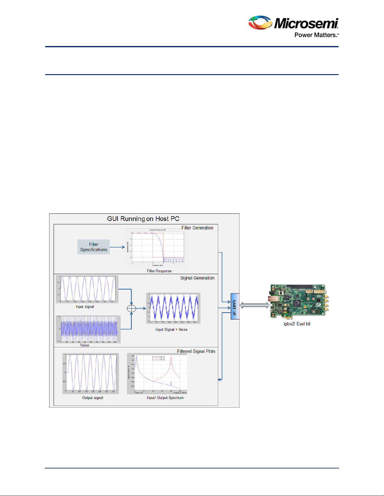
Figure 1 shows the top-level diagram for the DSP FIR filter demo.
Figure 1 • Top-Level Diagram of DSP FIR Filter Demo
Revision 6 6
Page 7
IGLOO2 FPGA DSP FIR Filter
'HVLJQ)LOHV
3URJUDPPLQJ)LOHV
,*/B),5B),/7(5B')
GRZQORDGBIROGHU!
*8,
5HDGPHW[W
2.2 Design Requirements
Table 1 lists the hardware and software requirements.
Table 1 • Design Requirements
Design Requirements Description
Hardware Requirements
IGLOO2 Evaluation Kit:
• FlashPro4 programmer
• USB A to Mini-B cable
Host PC or Laptop Windows 7 64-bit Operating System
Software Requirements
®
Libero
FlashPro Programming Software v11.7
Host PC Drivers USB to UART drivers
Framework Microsoft .NET Framework 4 Client for launching demo GUI
system-on-chip (SoC) v11.7
Rev C or later
2.3 Demo Design
2.3.1 Introduction
The design files are available for download from the following path in the Microsemi website:
http://soc.microsemi.com/download/rsc/?f=m2gl_dg0504_dsp_fir_filter_liberov11p7_df
The design files include:
• Design Files
•GUI
• Programming file
• Readme.txt file
Figure 2 shows the top-level structure of the design files. Refer to the Readme.txt file provided in the
demo file folder for the complete directory structure.
Figure 2 • Demo Design Files Top-Level Structure
Revision 6 7
Page 8
IGLOO2 FPGA DSP FIR Filter
'DWD+DQGOH
)LOWHU&RQWURO
)60
),5,1%XIIHU ),5287%XIIHU ),55HDO%XIIHU
))7,PDJLQDU\
%XIIHU
&RUH),5 &RUH))7
&RHI
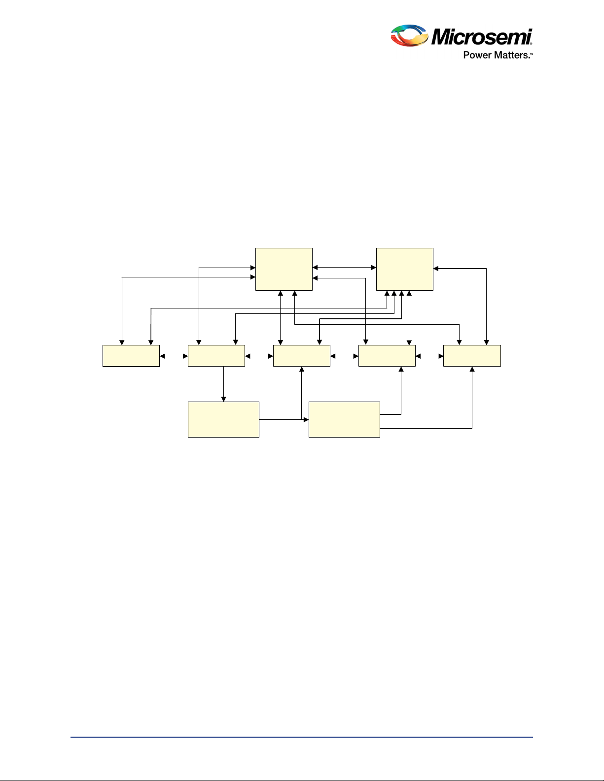
2.3.2 Demo Design Description
This demo design uses the following blocks:
• Data Handle (user RTL)
• Filter Control (user RTL)
• TPSRAM IP (IPcore)
• CoreUART(IPcore)
• CoreFIR (IPcore)
• CoreFFT (IPcore)
• SYSRESET (IPcore)
• OSC (IPcore)
• CCC (IPcore)
Figure 3 shows the detailed block diagram of the demo design.
Figure 3 • DSP FIR Filter Demo Design Block Diagram
2.3.2.1 Data Handle
Data handle consists of the Core UART IP and the UART interface finite state machine handling the
control operations between the host PC (GUI interface) and the fabric logic. Control operations include
the loading of filter coefficients, filter input data to the corresponding input data buffer, coefficient buffers,
and send and receive data from the Host PC GUI.
2.3.2.2 Filter Control
Controls the FIR filter and the FFT operations. It loads the filtered data to the corresponding output buffer
and moves the FFT output data to the corresponding output data buffer.
Revision 6 8
Page 9
IGLOO2 FPGA DSP FIR Filter
2.3.2.3 TPSRAM IP
TPSRAM IP uses the following configurations:
• Filter coefficient buffer
• Input signal data buffer
• Output signal buffer
• Output signal FFT real data buffer
• Output signal FFT imaginary data buffer
Table 2 • TPSRAM Configuration for Data Buffers
Buffer Write Port Read Port
Depth Width Depth Width
Filter Coefficients 64 8 32 16
FIR Input Signal 2048 8 1024 16
FIR Output Signal 1024 16 1024 16
FFT Output Real Signal 256 16 256 16
FFT Output Imaginary Signal 256 16 256 16
2.3.2.4 CoreUART
The Core UART IP is used to transfer the data between the host PC (GUI) and IGLOO2. The Core UART
configuration is as follows:
• Version: 5.5.101
• TxFIFO: Disable TxFIFO
• RxFIFO: Disable RxFIFO
• RxLegacyMode: Disable
• Baud rate: 115200
• Number of bits: 8
•Stop bits: 1
• Parity: None
2.3.2.5 CoreFIR
The Core FIR IP is used in the Reloadable coefficient mode to support Low-pass, High-pass, Band-pass,
and Band-reject filters. The Core FIR IP configuration is as follows:
• Version: 8.6.101
• Filter Type: Single rate fully enumerated
• Number of Taps: 31
• Coefficients Type: Reloadable
• Coefficients Bit Width: 16 (signed)
• Data Bit Width: 16 (signed)
• Filter Structure: Transposed with symmetry
2.3.2.6 CoreFFT
The Core FFT IP is used for generating the frequency spectrum of the filtered data. Core FFT IP
configuration is as follows:
• Version: 6.4.105
• FFT Architecture: In place
• FFT Type: Forward
• FFT Scaling: Conditional
• FFT Transform Size: 256
• Width: 16
Revision 6 9
Page 10
IGLOO2 FPGA DSP FIR Filter
2.3.2.7 SYSRESET
The SYSRESET IP provides the power on reset signal.
2.3.2.8 OSC
The OSC IP is configured as an RC oscillator to provide the 50 MHz signal to the clock conditioning
circuit (CCC).
2.3.2.9 CCC
The CCC IP is configured to provide a 150 MHz clock signal. For detailed smart design implementation
and resource usage summary, refer to "Appendix: SmartDesign Implementation" on page 30.
2.4 Setting Up the Demo Design
The following steps describe how to setup the hardware demo:
1. Connect the jumpers on the IGLOO2 Evaluation Kit board, as shown in Ta bl e 3 .
Table 3 • IGLOO2 FPGA Evaluation Kit Jumper Settings
Jumper Pin (From) Pin (To) Comments
J22 1 2 Default
J23 1 2 Default
J24 1 2 Default
J8 1 2 Default
J3 1 2 Default
CAUTION: While making the jumper connections, the power supply switch SW7 must be switched
OFF.
2. Connect the Power supply to the J6 connector, switch ON the power supply switch, SW7.
3. Connect the FlashPro4 programmer to the J5 connector of the IGLOO2 Evaluation Kit board.
4. Connect the host PC USB port to the J18 USB connector on the IGLOO2 Evaluation Kit board using
the USB Mini-B cable.
Revision 6 10
Page 11
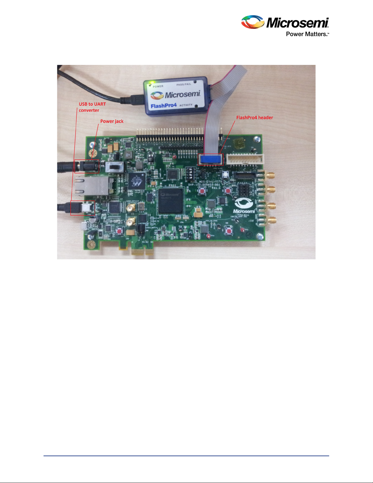
IGLOO2 FPGA DSP FIR Filter
Figure 4 shows the board setup for running the DSP FIR Filter demo on the IGLOO2 Evaluation Kit.
Figure 4 • IGLOO2 Evaluation Kit DSP FIR Filter Demo Setup
Revision 6 11
Page 12

IGLOO2 FPGA DSP FIR Filter
5. Ensure that the USB to UART bridge drivers are automatically detected. This can be verified in the
Device Manager of the host PC. The FTDI USB to UART converter enumerates four COM ports.
For USB 2.0, note down the USB Serial Converter D COM port number to use it in the
IGL2_FIR_Filter.exe. Figure 5 shows the USB 2.0 Serial port properties and the connected
COM10 and USB Serial Converter D.
Figure 5 • USB to UART Bridge Drivers
6. If the USB to UART bridge drivers are not installed, download and install the drivers from
www.microsemi.com//documents/CDM_2.08.24_WHQL_Certified.zip.
Revision 6 12
Page 13

IGLOO2 FPGA DSP FIR Filter
2.5 Programming the Demo Design
The following steps describe how to program the demo design:
1. Download the demo design from:
http://soc.microsemi.com/download/rsc/?f=m2gl_dg0504_dsp_fir_filter_liberov11p7_df
2. Switch ON the power supply switch, SW7.
3. Launch the FlashPro software.
4. Click New Project.
5. In the New Project window, enter the project name as IGL2_FIR_FILTER.
Figure 6 • FlashPro - New Project
6. Click Browse and navigate to the location where you want to save the project.
7. Select Single device as the Programming mode.
8. Click OK to save the project.
Revision 6 13
Page 14

IGLOO2 FPGA DSP FIR Filter
2.5.1 Setting Up the Device
The following steps describe how to configure the device:
1. Click Configure Device on the FlashPro GUI.
2. Click Browse and navigate to the location where the IGL2_FIR_FILTER.stp file is located and
select the file. The default location of the programming file is:
<download_folder>\IGL2_FIR_FILTER_DF\ProgrammingFiles\IGL2_FIR_FILTER.stp.
3. Click Open. The required programming file is selected and is ready to be programmed in the device.
4. Select Advanced as Mode and PROGRAM as Action.
2.5.2 Programming the Device
Figure 7 • FlashPro Project Configuration
Revision 6 14
Page 15

IGLOO2 FPGA DSP FIR Filter
5. Click PROGRAM to start programming the device. Wait until Programmer Status is changed to
RUN PASSED.
Figure 8 • FlashPro Project RUN Passed
Revision 6 15
Page 16

IGLOO2 FPGA DSP FIR Filter
2.5.3 DSP FIR Demo GUI
The DSP FIR demo is provided with a user-friendly GUI that runs on the host PC which communicates
with the IGLOO2 Evaluation Kit. The UART is used as the underlying communication protocol between
the host PC and IGLOO2 Evaluation Kit.
Figure 9 shows the DSP FIR demo GUI.
Figure 9 • DSP FIR Demo Window
The DSP FIR demo window consists of the following tabs:
• Input Parameters: Configures the serial COM port, filter generation, and signal generation.
• Filter Input: Plots the input signal and its frequency spectrum
• Filter Output: Plots the output signal and its frequency spectrum
• Text Viewer: Shows the coefficients, input signal, output signal, and FFT data values
Click Help for more information on the GUI.
Revision 6 16
Page 17

IGLOO2 FPGA DSP FIR Filter
2.6 Running the Demo Design
The following steps describe how to run the demo design:
1. Launch the DSP FIR Demo GUI executable file available in the design files.
(\IGL2_FIR_FILTER_DF\GUI\IGL2_FIR_Filter.exe). The FIR Filter Demo window is displayed, as
shown in Figure 10.
Figure 10 • Serial Port Configuration
2. Serial Port Configuration: The COM port number is automatically detected and the baud rate is
fixed at 115200. Click Connect. Refer to Figure 10.
Revision 6 17
Page 18

IGLOO2 FPGA DSP FIR Filter
3. Filter Generation: Two options are provided for generating the filter coefficients:
• Generate the coefficients using MATLAB or any similar tool and save it as a text file (Refer to
"Appendix: Coefficient Text File Format" on page 32 for the format of the text file). The GUI can
be used to browse and load this file. Refer to Figure 11.
Figure 11 • Filter Generation - 1
Revision 6 18
Page 19

IGLOO2 FPGA DSP FIR Filter
• Generate the Filter coefficients using the GUI.
The following parameters are required to generate filter coefficients:
• Filter Type: Low-pass (Low-pass/High-pass/Band-pass/Band-reject filter)
• Filter Window: Blackman (Blackman/Hamming window)
• Low Cut-off Frequency: Disabled for Low-pass filter required (high cut-off frequency is
disabled for high-pass filter)
• High Cut-off Frequency: 20 MHz
• Filter Taps: 31 (Fixed)
Press Generate Filter to generate the filter coefficients.
Figure 12 • Filter Generation - 2
Revision 6 19
Page 20

IGLOO2 FPGA DSP FIR Filter
4. The successful after-generation graphs of the filter coefficients, filter response, and the filter
coefficient plots, are displayed. Refer to Figure 13.
Figure 13 • Filter Response and Filter Coefficient Plot
Revision 6 20
Page 21

IGLOO2 FPGA DSP FIR Filter
• The following parameters are required to generate Signal Generation:
• Sampling Frequency: 150 MHz (Fixed)
• Number of Samples: 1024 (Fixed)
• Input Frequency 1: Enter the signal frequency in the Pass-band region. For example, 1 MHz to
High cut-off frequency
• Input Frequency 2: Enter the signal frequency in the Stop-band region. For example, High
cut-off frequency to Sampling frequency/2
5. Click Generate Signal, as shown in Figure 14.
Figure 14 • Signal Generation
Revision 6 21
Page 22

IGLOO2 FPGA DSP FIR Filter
6. Input signal and frequency spectrum of the specified signal are displayed, as shown in Figure 15.
Figure 15 • Input Signal and Input Signal FFT Plot
Revision 6 22
Page 23

IGLOO2 FPGA DSP FIR Filter
7. To configure the input frequencies and coefficients, click Start, as shown in Figure 16. It sends the
input data (1K samples) and filter coefficients to the IGLOO2 device for processing the filtering
operation.
Figure 16 • DSP FIR Filter Demo - Start
Revision 6 23
Page 24

IGLOO2 FPGA DSP FIR Filter
After completing the filter operation by the IGLOO2 device, the GUI plots the filtered data and the
FFT data on the filter output window, as shown in Figure 17. Since Low-pass filter option was
selected, the High frequency component is suppressed while the Low frequency signal is preserved.
This can be observed in the frequency spectrum of the output signal.
Figure 17 • Filtered Signal: Time and Frequency Plot
Revision 6 24
Page 25

IGLOO2 FPGA DSP FIR Filter
8. Right-click on the window, it shows different options, as shown in Figure 18. The data can be copied,
saved, and exported to the CSV plot for analysis purpose. Page setup, print, show point values,
zoom, and set scale are set to default.
Figure 18 • Filtered Signal: GUI Options
Revision 6 25
Page 26

IGLOO2 FPGA DSP FIR Filter
9. The filter coefficients, input signal, output signal, and FFT output data values can be viewed in the
Text viewer. Click Text Viewer and click the corresponding View, as shown in Figure 19.
Figure 19 • Text Viewer
Revision 6 26
Page 27

IGLOO2 FPGA DSP FIR Filter
The values can be observed, as shown in Figure 20.
Figure 20 • Text Viewer: Filter Coefficient Values
Revision 6 27
Page 28

IGLOO2 FPGA DSP FIR Filter
10. To save the coefficients as a text file, right-click Filter Coefficients window, it shows different
options, as shown in Figure 21. Click Save and select OK to save the text file.
Figure 21 • Text Viewer: Coefficients Save Options
Revision 6 28
Page 29

IGLOO2 FPGA DSP FIR Filter
11. Click Exit to stop the demo, as shown in Figure 22.
Figure 22 • FIR Filter Demo: Exit
2.7 Conclusion
This demo shows the features of the IGLOO2 device including mathblocks and LSRAMS for DSP
specific applications. Also provides information about how to use the Microsemi DSP IP cores (CoreFIR,
and CoreFFT). This FIR Filter GUI-based demo is very easy to use and provides several options to
understand and implement the DSP filters on the IGLOO2 device.
Revision 6 29
Page 30

Appendix: SmartDesign Implementation
3 Appendix: SmartDesign Implementation
DSP FIR filter SmartDesign is shown in Figure 23.
Figure 23 • DSP FIR Filter SmartDesign
Table 4 shows SmartDesign blocks in DSP FIR Filter.
Table 4 • DSP FIR Filter Demo SmartDesign Blocks and Description
S.No Block Name Description
1 DATA_HANDLE_0 Handles the communication between the host PC and the IGLOO2
Evaluation Kit board.
2 FILTERCONTROL_FSM_0 Control logic to generate the control signals for the FIR and FFT
operations.
3 Coef_Buff IP for the filter coefficient buffer.
4 FIR_IN_Buff IP for the FIR input signal data buffer.
FIR_Out_Buff IP for the FIR output signal buffer.
FFT_Re_Buff IP for the FFT output imaginary data buffer.
FFT_Im_Buff IP for the FFT output real data buffer.
5 COREFIR_0 COREFIR IP
6 COREFFT_0 COREFFT IP
7 SYSRESET_0 Reset IP
8 OSC_0 Oscillator IP
9 FCCC_0 Clock Conditioning circuit IP
Revision 6 30
Page 31

Appendix: Resource Usage Summary
4 Appendix: Resource Usage Summary
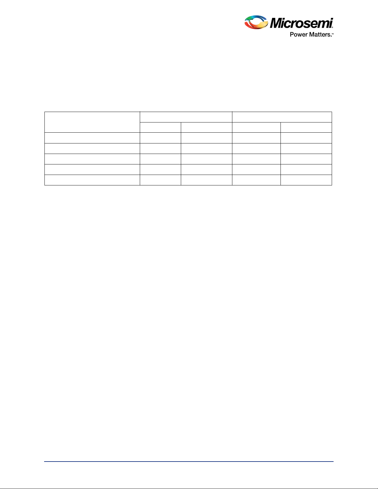
Table 5 shows DSP FIR filter resource usage summary.
Device: IGLOO2 device
Die: M2GL010
Package: 484 FBGA
Table 5 • DSP FIR Filter Demo Resource Usage Summary
Type Used Total Percentage
4LUT 2867 12084 23.73
DFF 3747 12084 31.01
RAM64x18 0 22 0.00
RAM1Kx18 12 21 57.14
MACC 20 22 90.91
Table 6 shows MACC blocks usage summary.
Table 6 • MACC Blocks Usage Summary
CoreFIR CoreFFT Total
16 04 20
Table 7 shows RAM1Kx18 blocks usage summary.
Table 7 • RAM1Kx18 Blocks Usage Summary
CoreFIR CoreFFT Fabric Buffers Total
07 5 12
Revision 6 31
Page 32

Appendix: Coefficient Text File Format
FRHIILFLHQWBVHWB
5 Appendix: Coefficient Text File Format
The FIR filter coefficients can be loaded from an ASCII text file (* .txt). Create the coefficient file using
a text editor. The format of the text file must be, as shown in Figure 24 . The coefficient values must be
entered as integer numbers. For a symmetric or anti-symmetric filter, only half of the coefficients must be
listed in the file (this applies to the fully enumerated type only). Only one coefficient value per line is
permitted. An extra empty line must be placed after the last coefficient of the last set.
Figure 24 • Coefficient File Example – 9 Taps, Decimal Values
Revision 6 32
Page 33

Revision History
6 Revision History
The following table shows important changes made in this document for each revision.
Revision Changes
Revision 6
(April 2016)
Revision 5
(October 2015)
Revision 4
(January 2015)
Revision 3
(August 2014)
Revision 2
(June 2014)
Revision 1
(January 2014)
Updated the document for Libero v11.7 software release (SAR 78044).
Updated the document for Libero v11.6 software release (SAR 72354).
Updated the document for Libero v11.5 software release (SAR 63927).
Updated the document for Libero v11.4 software release (SAR 59681).
Updated the document for Libero v11.3 software release (SAR 56265).
Figure 3 on page 8 was updated.
Initial release
Revision 6 33
Page 34

Product Support
7 Product Support
Microsemi SoC Products Group backs its products with various support services, including Customer
Service, Customer Technical Support Center, a website, electronic mail, and worldwide sales offices.
This appendix contains information about contacting Microsemi SoC Products Group and using these
support services.
7.1 Customer Service
Contact Customer Service for non-technical product support, such as product pricing, product upgrades,
update information, order status, and authorization.
From North America, call 800.262.1060
From the rest of the world, call 650.318.4460
Fax, from anywhere in the world, 408.643.6913
7.2 Customer Technical Support Center
Microsemi SoC Products Group staffs its Customer Technical Support Center with highly skilled
engineers who can help answer your hardware, software, and design questions about Microsemi SoC
Products. The Customer Technical Support Center spends a great deal of time creating application
notes, answers to common design cycle questions, documentation of known issues, and various FAQs.
So, before you contact us, please visit our online resources. It is very likely we have already answered
your questions.
7.3 Technical Support
For Microsemi SoC Products Support, visit
http://www.microsemi.com/products/fpga-soc/design-support/fpga-soc-support.
7.4 Website
You can browse a variety of technical and non-technical information on the Microsemi SoC Products
Group home page, at http://www.microsemi.com/products/fpga-soc/fpga-and-soc.
7.5 Contacting the Customer Technical Support Center
Highly skilled engineers staff the Technical Support Center. The Technical Support Center can be
contacted by email or through the Microsemi SoC Products Group website.
7.5.1 Email
You can communicate your technical questions to our email address and receive answers back by email,
fax, or phone. Also, if you have design problems, you can email your design files to receive assistance.
We constantly monitor the email account throughout the day. When sending your request to us, please
be sure to include your full name, company name, and your contact information for efficient processing of
your request.
The technical support email address is soc_tech@microsemi.com.
7.5.2 My Cases
Microsemi SoC Products Group customers may submit and track technical cases online by going to My
Cases.
Revision 6 34
Page 35

Product Support
7.5.3 Outside the U.S.
Customers needing assistance outside the US time zones can either contact technical support via email
(soc_tech@microsemi.com) or contact a local sales office. Visit About Us for sales office listings and
corporate contacts.
7.6 ITAR Technical Support
For technical support on RH and RT FPGAs that are regulated by International Traffic in Arms
Regulations (ITAR), contact us via soc_tech@microsemi.com. Alternatively, within My Cases, select Yes
in the ITAR drop-down list. For a complete list of ITAR-regulated Microsemi FPGAs, visit the ITAR web
page.
Revision 6 35
Page 36

Microsemi Corporate
Headquarters
One Enterprise, Aliso Viejo,
CA 92656 USA
Within the USA: +1 (800) 713-4113
Outside the USA: +1 (949) 380-6100
Sales: +1 (949) 380-6136
Fax: +1 (949) 215-4996
E-mail: sales.support@microsemi.com
© 2016 Microsemi Corporation. All
rights reserved. Microsemi and the
Microsemi logo are trademarks of
Microsemi Corporation. All other
trademarks and service marks are the
property of their respective owners.
Microsemi Corporation (Nasdaq: MSCC) offers a comprehensive portfolio of semiconductor
and system solutions for communications, defense & security, aerospace and industrial
markets. Products include high-performance and radiation-hardened analog mixed-signal
integrated circuits, FPGAs, SoCs and ASICs; power management products; timing and
synchronization devices and precise time solutions, setting the world's standard for time; voice
processing devices; RF solutions; discrete components; enterprise storage and communication
solutions, security technologies and scalable anti-tamper products; Ethernet solutions; Powerover-Ethernet ICs and midspans; as well as custom design capabilities and services.
Microsemi is headquartered in Aliso Viejo, Calif, and has approximately 4,800 employees
globally. Learn more at www.microsemi.com.
Microsemi makes no warranty, representation, or guarantee regarding the information contained herein or
the suitability of its products and services for any particular purpose, nor does Microsemi assume any
liability whatsoever arising out of the application or use of any product or circuit. The products sold
hereunder and any other products sold by Microsemi have been subject to limited testing and should not
be used in conjunction with mission-critical equipment or applications. Any performance specifications are
believed to be reliable but are not verified, and Buyer must conduct and complete all performance and
other testing of the products, alone and together with, or installed in, any end-products. Buyer shall not rely
on any data and performance specifications or parameters provided by Microsemi. It is the Buyer's
responsibility to independently determine suitability of any products and to test and verify the same. The
information provided by Microsemi hereunder is provided “as is, where is” and with all faults, and the entire
risk associated with such information is entirely with the Buyer. Microsemi does not grant, explicitly or
implicitly, to any party any patent rights, licenses, or any other IP rights, whether with regard to such
information itself or anything described by such information. Information provided in this document is
proprietary to Microsemi, and Microsemi reserves the right to make any changes to the information in this
document or to any products and services at any time without notice.
50200504-6/4.16
 Loading...