Microsemi Corporation 723J, 723F Datasheet

SG723
4/90 Rev 1.2 6/97 LINFINITY Microelectronics Inc.
Copyright 1997 11861 Western Avenue
∞ ∞
∞ ∞
∞ Garden Grove, CA 92841
1 (714) 898-8121
∞∞
∞∞
∞ FAX: (714) 893-2570
DESCRIPTION
This monolithic voltage regulator is designed for use with either positive
or negative supplies as a series, shunt, switching, or floating regulator
with currents up to 150mA. Higher current requirements may be
accommodated through the use of external NPN or PNP power
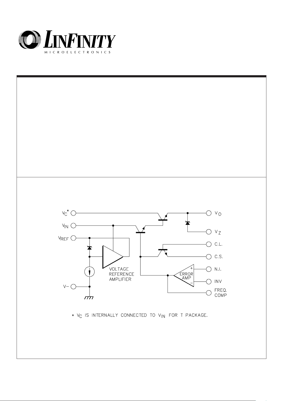
transistors. This device consists of a temperature compensated
reference amplifier, error amplifier, power series pass transistor, current
limit, and remote shutdown circuitry.
The SG723 will operate over the full military ambient temperature range
of -55°C to 125°C.
PRECISION VOLTAGE REGULATOR
FEATURES
••
••
• Positive or negative supply operation
••
••
• Series, shunt, switching or floating operation
••
••
• Low line and load regulation
••
••
• Output adjustable from 2V to 37V
••
••
• Output current to 150 mA
••
••
• Low standby current drain
••
••
• 0.002%/°C average temperature variation
HIGH RELIABILITY FEATURES - SG723
♦♦
♦♦
♦ Available to MIL-STD-883 and DESC SMD
♦♦
♦♦
♦ MIL-M38510/10201BHA - JAN 723F
♦♦
♦♦
♦ MIL-M38510/10201BIA - JAN 723T
♦♦
♦♦
♦ MIL-M38510/10201BCA - JAN723J
♦♦
♦♦
♦ Radiation data available
♦♦
♦♦
♦ LMI level "S" processing available
BLOCK DIAGRAM

SG723
4/90 Rev 1.2 6/97 LINFINITY Microelectronics Inc.
Copyright 1997 11861 Western Avenue
∞ ∞
∞ ∞
∞ Garden Grove, CA 92841
2 (714) 898-8121
∞∞
∞∞
∞ FAX: (714) 893-2570
Pulse (50 ms) Input Voltage from VIN to V- .........................
Continuous Input Voltage from V
IN
to V- .............................
Input to Output Voltage Differential ....................................
Maximum Output Current ..............................................
Current from V
Z
(J-Package only)...................................
ABSOLUTE MAXIMUM RATINGS (Note 1)
Current from V
REF
...............................................................
Operating Junction Temperature
Hermetic (T, J, F, L-Packages).....................................
Storage Temperature Range ...........................
Lead Temperature (Soldering, 10 Seconds) .................
15mA
150°C
-65°C to 150°C
300°C
50V
40V
40V
150mA
25 mA
Note 1. Exceeding these ratings could cause damage to the device.
THERMAL DATA
J Package:
Thermal Resistance-
Junction to Case, θ
JC
.................. 30°C/W
Thermal Resistance-
Junction to Ambient, θ
JA
.............. 80°C/W
T Package:
Thermal Resistance-
Junction to Case, θ
JC
.................. 25°C/W
Thermal Resistance-
Junction to Ambient, θ
JA
........... 130°C/W
F Package:
Thermal Resistance-
Junction to Case, θ
JC
................... 80°C/W
Thermal Resistance-
Junction to Ambient, θ
JA
........... 145°C/W
L Package:
Thermal Resistance-
Junction to Case, θ
JC
.................. 35°C/W
Thermal Resistance-
Junction to Ambient, θ
JA
........... 120°C/W
Note A. Junction Temperature Calculation: TJ = TA + (PD x θJA).
Note B. The above numbers for
θJC are maximums for the limiting
thermal resistance of the package in a standard mounting configuration. The θ
JA
numbers are meant to be
guidelines for the thermal performance of the device/pcboard system. All of the above assume no ambient
airflow.
Input Voltage Range .................................
Output Current Range ........................................
Reference Current.............................................................
(V
OUT
+4.5V) to 38 V
5mA to 45mA
5mA
Zener Current (J-Package only).........................................
Operating Ambient Temperature Range
SG723 ..........................................................
5mA
-55°C to 125°C
RECOMMENDED OPERATING CONDITIONS (Note 2)
Note 2. Range over which the device is functional.
ELECTRICAL CHARACTERISTICS
(Unless otherwise specified, these specifications apply for the operating ambient temperature of TA = 25°C, VIN = VC = 12V, V- = 0V, V
OUT
= 5V, IL =
1 mA, R
SC
= 0Ω, C1 = 100pF, and divider impedance as seen by error amplifier ≤ 10KΩ. Low duty cycle pulse testing echniques are used which maintains
junction and case temperatures equeal to the ambient temperature.)
Test ConditionsParameter
Input Voltage Range
Output Voltage Range
Input to Output Differential
Line Regulation
(Note 3)
Load Regulation (Note 3)
Ripple Rejection
Temperature Stability
(Note 4)
Short Circuit Current Limit
Reference Voltage
Output Noise Voltage
Standby Current Drain
Long Term Stability
Units
V
V
V
%V
OUT
%V
OUT
%V
OUT
%V
OUT
%V
OUT
dB
dB
%/°C
mA
V
µV
rms
µV
rms
mA
%/Khr
V
IN
= 12V to 15V
T
A
= T
MIN
to T
MAX
VIN = 12V to 40V
I
L
= 1 to 50 mA
T
A
= T
MIN
to T
MAX
f = 50 Hz to 10KHz
C
REF
= 0
C
REF
= 5µF
T
A
= T
MIN
to T
MAX
RSC = 10Ω
BW = 100Hz to 10KHz
C
REF
= 0
C
REF
= 5µF
I
L
= 0, VIN = 30V
Note 4. These parameters, although guaranteed,
are not tested in production.
Note 3. Applies for constant junction temperature. Temperature drift effects must be taken
into account separately when the unit is operating under conditions of high dissipation.
SG723
Min. Typ. Max.
40
37
38
0.1
0.3
0.2
0.15
0.6
0.015
7.35
3.5
0.01
0.02
0.03
74
86
0.002
65
7.15
20
2.5
2.3
0.1
9.5
2.0
3.0
6.95
 Loading...