Microsemi Corporation 2N7372 Datasheet

SYMBOL
CHARACTERISTIC
2N7372
2N7373
UNITS
CBO
Collector-Base Voltage
- 100
100
V
C
Continuous Collector Current
55A
Peak Collector Current
1010A
Continuous Base Current
22A
STG
Storage Temperature
-65 to 200
Unclamped Inductive Load Energy
15
mj
FEATURES:FEATURES:
APPLICATIONS:APPLICATIONS:
• Power Supply
7516 Central Industrial Drive
DESCRIPTION:DESCRIPTION:
• Inverters and Converters
• General Purpose Amplifiers
Riviera Beach, Florida
33404
PHONE: (561) 842-0305
FAX: (561) 845-7813
2N7372 - PNP
2N7373 - NPN
Complimentary
• Planar Process for Reliability
• Fast Switching
• High-Frequency Power Transistors
• For Complementary Use with Each Other
• 15 mj Reverse Energy Rating with I
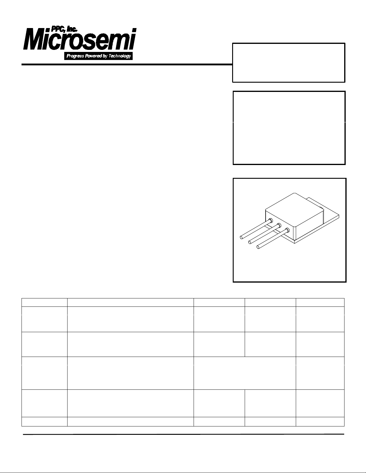
• Similar to 2N5004 and 2N5005 but JEDEC TO-254AA Package
• Leads can be Formed
• All Terminals Isolated from the Case
These power transistors are produced by PPC's MULTIPLE DIFFUSED
PLANAR process. This technology produces high voltage devices with
excellent switching speeds, frequency response, gain linearity, saturation
voltages, high current gain, and safe operating areas. These devices have
excellent unclamped and clamped reverse energy ratings with the base to
emitter reversed biased.
Ultrasonically bonded wire leads and gold eutectic die bonding are utilized to
permit operating temperature to 200°°C. The hermetically sealed package
insures maximum reliability and long life. The isolated low profile package
allows for easy PC board fit.
= 10MA and 4 V Reverse Bias
C
Power Transistors
in Hermetic Isolated
TO-254AA Packages
JAN/TX/TXV/JANS
TO-254AA
ABSOLUTE MAXIMUM RATINGS:ABSOLUTE MAXIMUM RATINGS:
V
V
CEO Collector-Emitter Voltage - 80 80 V
V
EBO
I
I
C
I
B
T
T
J Operating Junction Temperature -65 to 200 °°C
MSC1343.PDF 010-29-99
P
T
θθJC
Emitter-Base Voltage - 5.5 5.5 V
°°C
Lead Temperature 1/16" from cast for 10 sec. 300 °°C
Continuous Device
Dissipation TC = 25°°C
TC = 100°°C
Thermal Resistance Junction to Case 3 3 °°C/W
58 58 W
33 33 W

ELECTRICAL CHARACTERISTICS:ELECTRICAL CHARACTERISTICS:
(25°°Case Temperature Unless Otherwise Noted)
SYMBOL CHARACTERISTIC TEST CONDITIONS
V
I
CEO
I
CES
I
CEX
I
EBO
CEO
Collector-Emitter Breakdown
Voltage
Collector Cutoff Current,
Base Open
Collector Cutoff
Current, Emitter-Base Short
Collector Cutoff Current
Emitter Cutoff
IC = 100 mA, I
I
= 0, V
B
V
= 100 V
CE
V
= 60 V
CE
V
= 60 V, VBE = 2 V, TC = 150°°C
BE
V
= 5.5 V, I
EB
CE
= 0
B
= 40 V
=0
C
2N7372 - PNP
2N7373 - NPN
VALUE
Min.
80 ---- V
---- 50
----
----
---- 500
----
Max.
1
1
1
Units
µA
mA
µA
µA
mA
HFE
V
BE
V
BE(sat)
V
CE(sat)
HFE
Ihfel
C
OBO
t
on
t
off
Current
Static Forward Current
Transfer Ratio
Base-Emitter Volatage
Base-Emitter Saturation
Voltage
Collector-Emitter Saturation
Voltage
Small Signal Common-
Emitter Forward Current
Transfer Ratio
Small Signal Common
Emitter Forward Current
Transfer Ratio
Open-Circuit Output
Capacitance
Turn-on Time ---- 0.5
Turn-off Time
V
= 4.0 V, I
EB
IC = 5.0 A, V
IC = 2.5 A, V
IC = 2.5 A, V
IC = 50 mA, V
IC = 2.5 A, V
IC = 2.5 A, IB = 0.25 A
IC = 5.0 A, IB = 0.5 A
IC = 5.0 A, IB = 0.5 A
IC = 2.5 A, IB = 0.25 A
V
= 5.0 V, I
CE
VCE = 5.0 V, I
VCB = 10 V, I
IC = 5.0 A, I
VBE (OFF) = 3.7V
=0
C
= 5.0 V
CE
= 5.0 V
CE
= 5.0 V, TC = -55°°C
CE
= 5.0 V
CE
= 5.0 V
CE
= 100 mA, F = 1.0 KHz
C
= 0.5A, F = 10 MHz
C
= 0A, F = 0.1 MHz
E
= IB2 = 0.5 A
B1
---40
70
25
50
---- 1.45 V
----
----
----
---50 ---- ----
7.0 ---- ----
---- 250 pF
---- 1.5
1
----
200
----
----
1.45
2.2
1.5
0.75
µµA
----
----
----
----
V
V
V
----
µµs
µµs
MSC1343.PDF 010-29-99
 Loading...