Microsemi Corporation 2N2369A Datasheet

580 Pleasant St.
Watertown, MA 02172
PH: (617) 926-0404
FAX: (617) 924-1235
2N2369A
Features
• Meets MIL-S-19500/317
• Collector-Base Voltage 40V
40 Volts
200mAmps
• Collector Current: 200 mA
• Fast Switching 30 nS
NPN
BIPOLAR
TRANSISTOR
Maximum Ratings
RATING SYMBOL MAX. UNIT
Collector-Emitter Voltage V
Collector-Emitter Voltage V
Collector-Base Voltage V
Emitter-Base Voltage V
Collector Current -- Continuous I
Total Device Dissipation
@ TA = 25oC
Derate above 25oC
Total Device Dissipation
@ TC = 25oC
Derate above 25oC
Operating Temperature Range T
Storage Temperature Range T
Thermal Resistance, Junction to Ambient
Thermal Resistance, Junction to Case
R
R
CEO
CES
CBO
EBO
P
P
θJA
θJC
C
D
D
J
S
15 Vdc
40 Vdc
40 Vdc
4.5 Vdc
200 mA
0.36
2.06
1.2
6.85
-65 + 200
-65 + 200
486
146
Watt
mW/oC
Watt
mW/oC
o
o
o
C
o
C
C/W
C/W
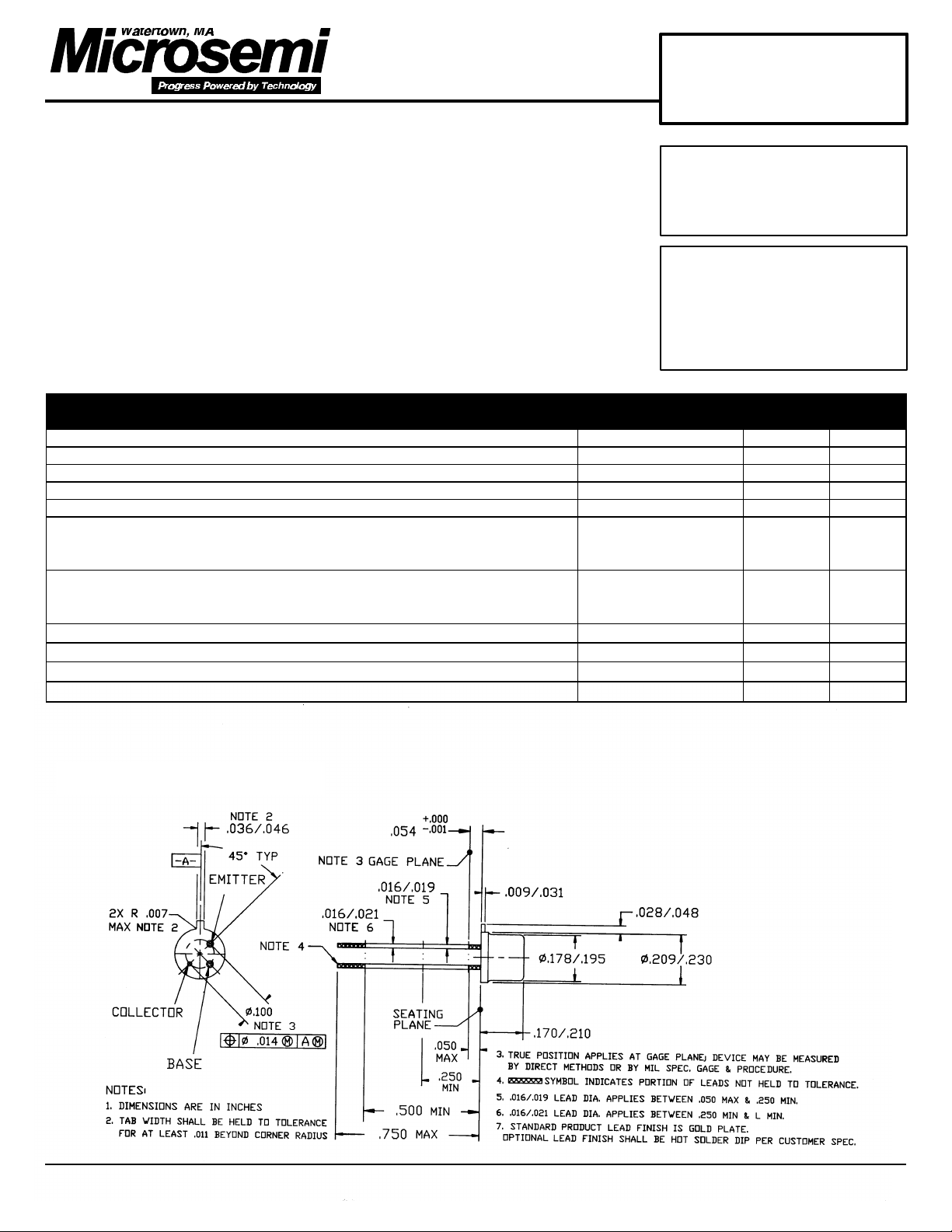
Mechanical Outline
Datasheet# MSC0277A 5/19/97

2N2369A
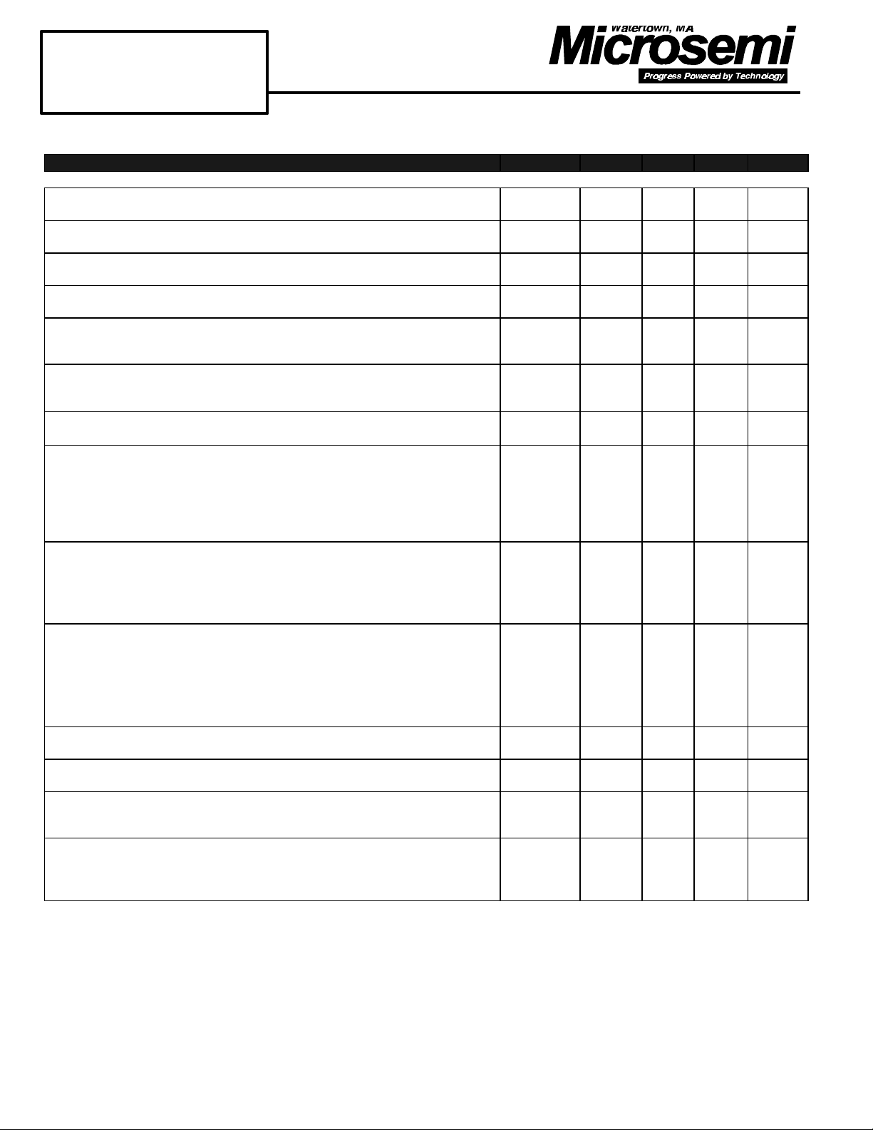
Electrical Parameters (TA @ 25°°C unless otherwise specified)
CHARACTERISTICS SYMBOL MIN. TYP. MAX. UNIT
Off Characteristics
Collector-Emitter Breakdown Voltage
(IC = 10 µA, VBE = 0)
Collector-Emitter Sustaining Voltage(1)
(IC = 10mAdc, IB = 0)
Collecter-Base Breakdown Voltage
(IC = 10 µA, IB = 0)
Emitter-Base Breakdown Voltage
(IC = 10 µA, IB = 0)
Collector Cutoff Current
(VCB = 20 Vdc)
Collector Emitter Cutoff Current
(VCE = 10 Vdc, VBE = 0.25Vdc)
@150C
Emitter Base Cutoff Current
(VEB = 4 Vdc )
D.C. Current Gain
(IC = 10 mAdc, VCE = 1.0 Vdc)
(IC = 10 mAdc, V
= 1.0 Vdc) @ -55C
CE
(IC = 10 mAdc, VCE = 0.35 Vdc)
(IC = 30 mAdc, VCE = 0.4 Vdc)
(IC = 100 mAdc, VCE = 1.0 Vdc)
Collector-Emitter Saturation Voltage(1)
(IC = 10 mAdc, IB = 1.0 mAdc)
(IC = 10mAdc, IB = 1.0 mAdc, TA = + 125oC)
(IC = 30 mAdc, IB = 3.0 mAdc)
(IC = 100 mAdc, IB = 10 mAdc)
Base-Emitter Saturation Voltage(1)
(IC = 10 mAdc, IB = 1.0 mAdc)
(IC = 10 mAdc, IB = 1.0 mAdc, TA = + 125oC)
(IC = 10 mAdc, IB 1.0 mAdc, TA = -55oC)
(IC = 30 mAdc, IB = 3.0 mAdc)
(IC = 100 mAdc, IB = 10 mAdc)
Small-signal short-circuit forward-current transfer ratio
(IC = 10 mAdc, VCE = 10 Vdc, f = 100 MHz)
Output Capacitance
(VCB = 5.0 Vdc, IE = 0, f = 1.0 MHz)
Input Capacitance
(VEB = 1.0 Vdc, IC = 0, f = 1.0 MHz)
BV
BV
BV
BV
I
I
I
V
CE(Sat)
V
BE(Sat)
/h
C
C
CES
CEX
EBO
h
OBO
CES
CEO
CBO
EBO
FE
fe/
IBO
40 -- Vdc
15 -- Vdc
40 -- Vdc
4.5 -- Vdc
-- 0.4
--
--
0.3
30
-- 0.25
40
20
40
30
20
--
--
--
--
0.70
0.59
--
--
--
120
---
120
120
120
0.20
0.30
0.25
0.45
0.85
--
1.02
0.9
1.20
5 10
-- 4.0
-- 5.0
µAdc
µAdc
µAdc
--
Vdc
Vdc
pf
pf
Switching Speeds, Turn-on Time
Storage Time
Turn-on Time
Turn-off Time
(1) Pulse Test: Pulse Width ≤ 300 ms, Duty Cycle ≤ 2.0 %.
Datasheet# MSC0277A 5/19/97
t
ns
s
t
on
t
off
--
--
--
13
12
18
 Loading...