Features
580 Pleasant St.
Watertown, MA 02172
PH: (617) 926-0404
FAX: (617) 924-1235
2N2221A
• Meets MIL 19500 /255
• Collector - Base Voltage 75 V
• Collector - Current 800 mA
• High Speed, Medium Current Bipolar Transistor
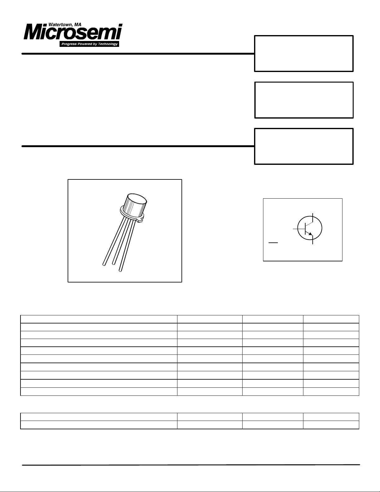
TO-18
SWITCHING
TRANSISTOR
JAN, JANTX, JANTXV
SMALL SIGNAL
BIPOLAR
NPN SILICON
COLLECTOR
BASE
EMITTER
Maximum Ratings
RATING SYMBOL VALUE UNIT
Collector - Emitter Voltage V
Collector - Base Voltage V
Emitter - Base Voltage V
Collector Current -- Continuous I
Total Device Dissipation @ TA = 25 °C
Derate above 25 °C
Total Device Dissipation @ TC = 25 °C
Derate above 25 °C
Operating Junction&Storage Temperature Range TJ, T
P
P
CEO
CBO
EBO
C
D
D
stg
- 65 to + 200
50 Vdc
75 Vdc
6 Vdc
800 mAdc
500 mW
2.85
1.8 WATTS
10.3
mW/°C
mW/°C
°C
Thermal Characteristics
CHARACTERISTIC SYMBOL MAX UNIT
Thermal Resistance, Junction to Ambient
MSCO328A 01-29-98 DSW2N2221A < - > ( 33807)
Rθ JA
350
°C/W

2N2221A
Electrical Characteristics (TA = 25°C unless otherwise noted)
OFF CHARACTERISTIC SYMBOL MIN MAX UNIT
Collector - Emitter Breakdown Voltage (1) V(BR)
( IC = 10 mA dc, IB = 0 ) 50 Vdc
Collector - Base Breakdown Voltage (1) V(BR)
( IC = 10 µAdc, IE = 0 )
Emitter - Base Breakdown Voltage (1) V(BR)
( IE = 10 µAdc, IC = 0 )
Collector - Emitter Cutoff Current I
( V
= 50 Vdc, V
CE
= 0 V ) 50 nAdc
BE(off)
Collector - Base Cutoff Current I
( VCB = 60 Vdc, IE = 0 ) 10 nAdc
( VCB = 60 Vdc, IE = 0, TA = 150 °C )
Emitter - Base Cutoff Current I
( VEB = 4 Vdc ) 10 nAdc
ON CHARACTERISTIC SYMBOL MIN MAX UNIT
DC Current Gain h
( IC = 100 µA dc, V
( IC = 1 mA dc, V
( IC = 10 mA dc, V
( IC = 150 mA dc, V
( IC = 500 mA dc, V
( IC = 10 mA dc, V
= 10 Vdc )
CE
= 10 Vdc ) 35 150
CE
= 10 Vdc ) 40
CE
= 10 Vdc ) (1) 40 120
CE
= 10 Vdc ) (1) 20
CE
= 10 Vdc, TJ = -55°C )
CE
Collector - Emitter Saturation Voltage V
( IC = 150 mAdc, IB = 15 mAdc ) (1) 0.3 Vdc
( IC = 500 mAdc, IB = 50 mAdc ) (1) 1.0 Vdc
Base - Emitter Saturation Voltage V
( IC = 150 mAdc, IB = 15 mAdc ) (1) 0.6 1.2 Vdc
( IC = 500 mAdc, IB = 50 mAdc ) (1) 2.0 Vdc
CES
CBO
EBO
FE
CE(sat)
BE(sat)
CEO
CBO
EBO
75 Vdc
6 Vdc
10
µAdc
30
15
1. Pulse Test: Pulse Width ≤ 300 µs, Duty Cycle ≤ 2.0%
MSCO328A 01-29-98 DSW2N2221A < - > ( 33807)

2N2221A
Electrical Characteristics (TA = 25°C unless otherwise noted)
SMALL - SIGNAL CHARACTERISTICS SYMBOL MIN MAX UNIT
Output Capacitance C
( V
= 10 Vdc, IE = 0, 100kHz ≤ f ≤ 1 MHz )
CB
Input Capacitance C
( V
= 0.5 Vdc, IC = 0, 100kHz ≤ f ≤ 1 MHz )
EB
SWITCHING CHARACTERISTICS SYMBOL MIN MAX UNIT
Turn - On Time t
( VCC = 30 Vdc, IC = 150 mAdc,
IB1 =15 mAdc) ( See FIGURE 1 ) 35 ns
Turn - Off Time t
( VCC = 30 Vdc, IC = 150 mAdc,
IB1 = - IB2 = 15 mAdc) ( See FIGURE 2 ) 300 ns
Small - Signal AC Characteristics (TA = 25°C)
LOW FREQUENCY SYMBOL MIN MAX UNIT
Common - Emitter Forward Current Transfer Ratio h
(IC = 1 mA, VCE = 10 V, f = 1kHz) 30
HIGH FREQUENCY
Common - Emitter Forward Current Transfer Ratio |hfe|
(IC = 20 mA, VCE = 20 V, f = 100 MHz) 2.5
obo
8 pF
ibo
25 pF
on
off
fe
S p i c e M o d e l (based upon typical device characteristics)
* 1
Q2N2221A NPN ( IS = 426.3f XTI = 3.0 EG = 1.11 VAF =250.3 BF = 72.14 ISE = 48.14p
+ NE = 2.935 IKF = 2.935 NK = 1.401 XTB = 1.5 BR = 11.49 ISC = 19.9f
+ NC = 1.88 IKR = 10.75 RC = 0.3567 CJC = 11.02p VJC = 0.3869 MJC = 0.3292
+ FC = 0.5 CJE = 29.31p VJE = 0.9036 MJE = 0.4101 TR = 16.89n TF = 537.5p
+ ITF = 0.1383 XTF = 84.83m VTF=10 )
*1. Microsemi Corp. claims no responsibility for misapplication of Spice Model information. Spice modeling should be
used as a precursor guide to in-circuit performance. Actual performance is the responsibility of the user/designer.
MSCO328A 01-29-98 DSW2N2221A < - > ( 33807)
 Loading...