Microsemi Corporation 28M0 Datasheet

NOTE 2: Pulsed: PW = 100ms max.; duty cycle
<
20%
28M0
A Microsemi Company
580 Pleasant St. Phone: 617-924-9280
Watertown, MA 02472 Fax: 617-924-1235
DIE SPECIFICATION
60V 300mA
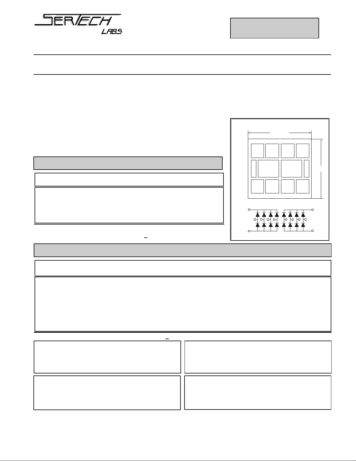
MONOLITHIC DIODE ARRAY
FEATURES:
• TWO EIGHT DIODE CORE DRIVER
.061"
J
J J J
• trr < 20 ns
• RUGGED AIR-ISOLATED CONSTRUCTION
• LOW REVERSE LEAKAGE CURRENT
Absolute Maximum Ratings:
Symbol Parameter Limit Unit
VBR(R) *1 *2 Reverse Breakdown Voltage 60 Vdc
IO *1 Continuous Forward Current 300 mAdc
IFSM *1 Peak Surge Current (tp= 1/120 s) 500 mAdc
Top Operating Junction Temperature Range -65 to +150 °C
Tstg Storage Temperature Range -65 to +200 °C
NOTE 1: Each Diode
A C
J JJJ
C A
Electrical Characteristics (Per Diode) @ 25°C unless otherwise specified
Symbol Parameter Conditions Min Max Unit
BV1 Breakdown Voltage IR = 10uAdc 60
Vf1 Forward Voltage IF = 100mAdc *1 1 Vdc
Vf2 Forward Voltage IF = 500mAdc *1 1.5 Vdc
IR1 Reverse Current VR = 40 Vdc 0.1 uAdc
Ct Capacitance (pin to pin) VR = 0 Vdc ; f = 1 MHz 8.0 pF
tfr Forward Recovery Time IF = 500mAdc 40 ns
trr Reverse Recovery Time IF = IR = 200mAdc, irr = 20 mAdc, RL = 100 ohms 20 ns
NOTE 1: Pulsed: PW = 300us +/- 50us, duty cycle < 2%, 90us after leading edge
Packaging Options:
W: Wafer (100% probed) U: Wafer (sample probed)
D: Chip (Waffle Pack) B: Chip (Vial)
V: Chip (Waffle Pack, 100% visually inspected) X: Other
Processing Options:
Standard: Capable of JANTXV application (No Suffix)
Suffix C: Commercial
Suffix S: Capable of S-Level equivalent applications
.054"
Metallization Options:
Standard: Al Top / Au Backside (No Dash #)
Sertech reserves the right to make changes to any product design, specification or other information at any time without prior
notice.
MSC1025.PDF Rev - 12/3/98
ORDERING INFORMATION
PART #: 28M0_ _- _
First Suffix Letter: Packaging Option
Second Suffix Letter: Processing Option
Dash #: Metallization Option
 Loading...