Microsemi Corporation 1N6511J, 1N6510F, 1N6101J, 1N6100F Datasheet

SG6100/SG6511
SG6101/SG6510
DESCRIPTION
The SG6100/SG6511 and SG6101/SG6510 diode arrays are monolithic,
high breakdown, fast switching speed diode arrays. The SG6100/SG6511
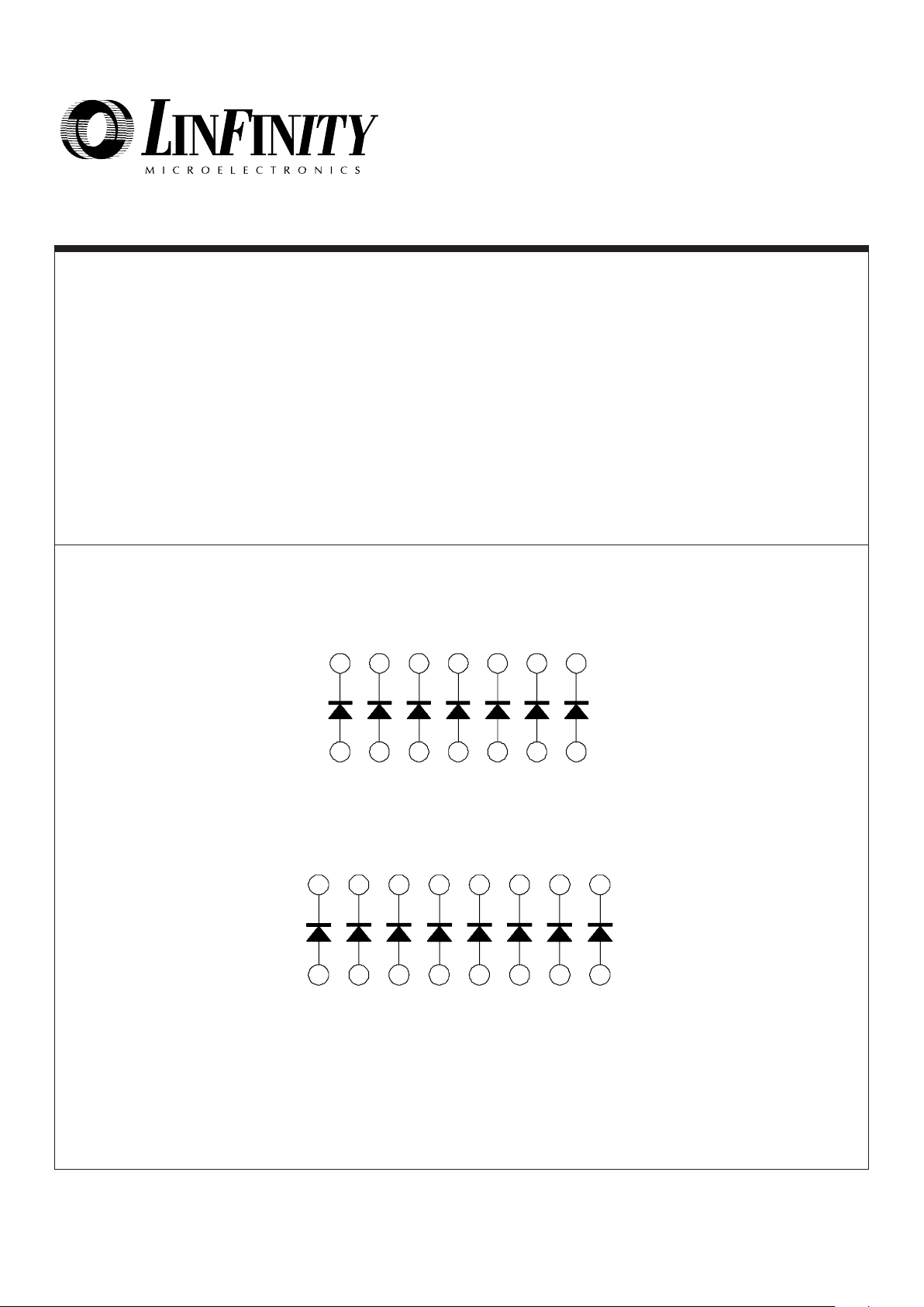
is configured with 7 straight through diodes, while the SG6101/SG6510 has
8 straight through diodes.
These two diode array configurations allow the designer maximum flexibility
for circuit design and board layout. Since each diode within the array has
individual anode and cathode connections the device may be used in a
variety of applications. Also, due to the array's monolithic construction the
diode electrical parameters are very closely matched.
Both devices are available in ceramic DIP and flatpack and can be processed
to Linfinity's S level, JANTXV, JANTX, or JAN equivalent flows.
DIODE ARRAY CIRCUITS
FEATURES
••
••
• 75V minimum breakdown voltage
••
••
• 100mA current capability per diode
••
••
• Switching speeds less than 5ns
••
••
• Low leakage current < 25nA
HIGH RELIABILITY FEATURES
♦♦
♦♦
♦ MIL-S-19500/474 QPL - 1N6100
- 1N6101
- 1N6510
- 1N6511
♦♦
♦♦
♦ Equivalent JANS, JANTXV, JANTX, JAN
screening available
CIRCUIT DIAGRAMS
7 - STRAIGHT THROUGH DIODES
SG6100/SG6511
8 - STRAIGHT THROUGH DIODES
SG6101/SG6510
6/91 Rev 1.1 2/94 LINFINITY Microelectronics Inc.
Copyright 1994 11861 Western Avenue
∞ ∞
∞ ∞
∞ Garden Grove, CA 92841
1 (714) 898-8121
∞∞
∞∞
∞ FAX: (714) 893-2570

DIODE ARRAY SERIES
6/91 Rev 1.1 2/94 LINFINITY Microelectronics Inc.
Copyright 1994 11861 Western Avenue
∞ ∞
∞ ∞
∞ Garden Grove, CA 92841
2 (714) 898-8121
∞∞
∞∞
∞ FAX: (714) 893-2570
ABSOLUTE MAXIMUM RATINGS (Note 1 & 2)
Breakdown Voltage (VBR) ....................................................
Output Current (I
O
), TC = 25°C
Continuous .................................................................
75V
300mA
Operating Junction Temperature
Hermetic (J, F Packages) ............................................
Storage Temperature Range ............................
Lead Temperature (Soldering, 10 seconds) ..................
150°C
-65°C to 200°C
300°C
Note 1. Exceeding these ratings could cause damage to the device.
Note 2. Applicable for each diode.
THERMAL DATA
J Package (14 & 16 Pin):
Thermal Resistance-
Junction to Case, θ
JC
.................. 30°C/W
Thermal Resistance-
Junction to Ambient, θ
JA
.............. 80°C/W
F Package (14 Pin):
Thermal Resistance-
Junction to Case, θ
JC
.................. 80°C/W
Thermal Resistance-
Junction to Ambient, θ
JA
........... 140°C/W
F Package (16 Pin):
Thermal Resistance-
Junction to Case, θ
JC
.................. 70°C/W
Thermal Resistance-
Junction to Ambient, θ
JA
........... 115°C/W
Note A. Junction Temperature Calculation: TJ = TA + (PD x θJA).
Note B. The above numbers for
θJC are maximums for the limiting
thermal resistance of the package in a standard mounting configuration. The θ
JA
numbers are meant to be
guidelines for the thermal performance of the device/pcboard system. All of the above assume no ambient
airflow.
Operating Ambient Temperature Range
SG6100 ..........................................................-55°C to 150°C
SG6101 ..........................................................-55°C to 150°C
Note 3. Range over which the device is functional.
RECOMMENDED OPERATING CONDITIONS (Note 3)
ELECTRICAL CHARACTERISTICS
(Unless otherwise specified, these specifications apply for the operating ambient temperature of TA = 25°C for each diode. Low duty cycle pulse testing
techniques are used which maintains junction and case temperatures equal to the ambient temperature.)
1.0
1.0
25
100
50
4
15
5
Min. Typ. Max.
V
V
V
nA
nA
µA
pf
ns
ns
IR = 5µA, Duty Cycle < 20%
Duty Cycle ≤ 2%, 300 µs pulse
I
F
= 100mA
I
F
= 10mA, TA = -55°C
V
R
= 20V
V
R
= 40V
V
R
= 40V, TA = 150°C
V
R
= 0V, f = 1MHz, Pin-to-pin
I
F
= 500mA, tr ≤ 15ns, Vfr = 1.8V, RS = 50Ω
I
F
= IR = 200mA, irr = 20mA, RL = 100Ω
Breakdown Voltage (V
BR
)
Forward Voltage (V
F
)
Reverse Current (I
R
)
Capacitance (C)
(Note 4)
Forward Recovery Time (tfr)
(Note 4)
Reverse Recovery Time (trr)
(Note 4)
75
Test Conditions UnitsParameter
Note 4. The parameters, although guaranteed, are not 100% tested in production.
SG6511 ..........................................................-55°C to 150°C
SG6510 ..........................................................-55°C to 150°C
SG6100/SG6511
SG6010/SG6510
 Loading...