NOTE 2: Pulsed: PW = 100ms max.; duty cycle
<
20%
NOTE 1: Pulsed: PW = 300us +/- 50us, duty cycle
<
2%, 90us after leading edge
Packaging Options:
Metallization Options:
Processing Options:
04M0
A Microsemi Company
580 Pleasant St. Phone: 617-924-9280
Watertown, MA 02472 Fax: 617-924-1235
DIE SPECIFICATION
100V 300mA
MONOLITHIC DIODE ARRAY
5
FEATURES:
• INDIVIDUAL DIODES EQUIVALENT TO 1N4148
• Vf MATCH TO 5 mV at 10 mA
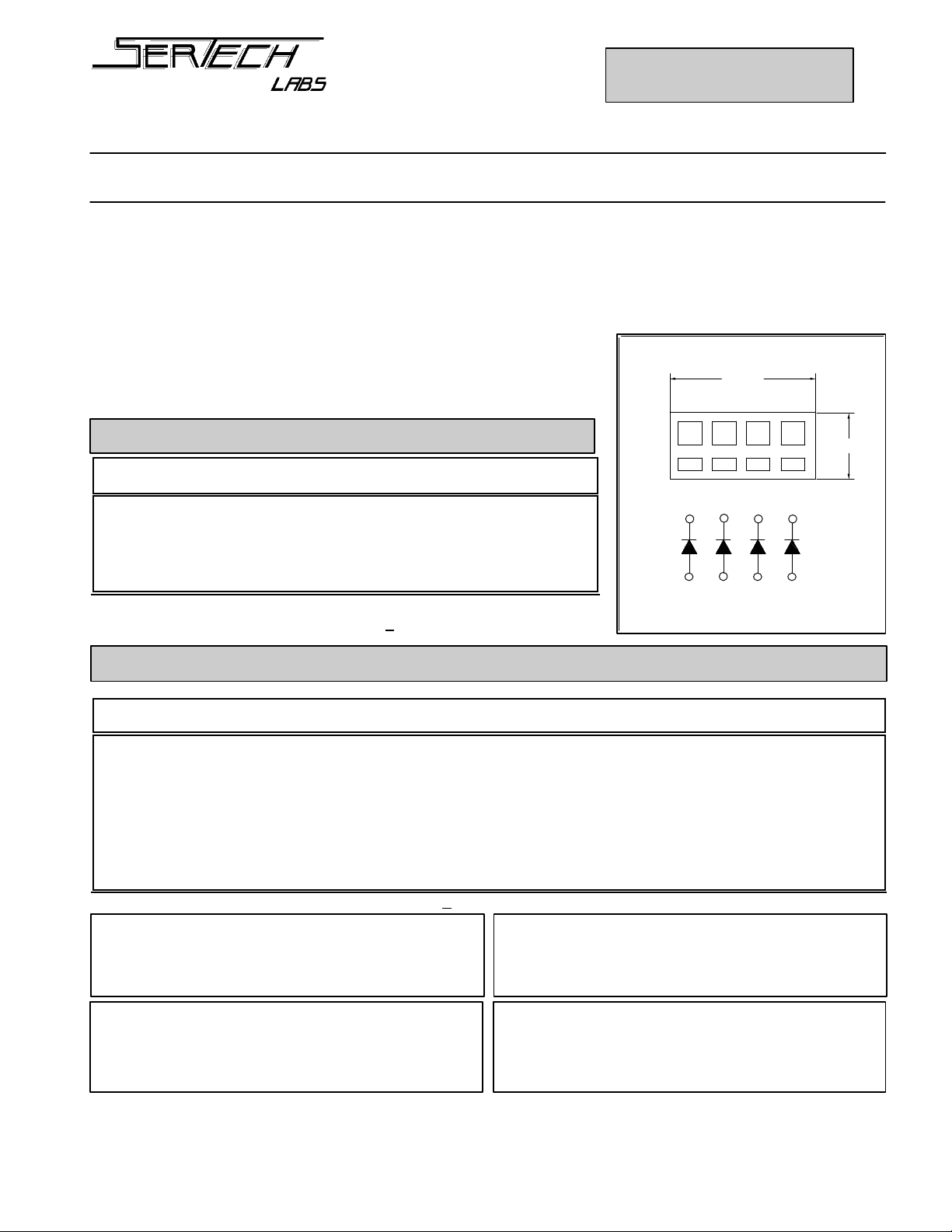
C C
A A
.049"
C
A A
C
.023"
• ULTRA-HIGH SPEED SWITCHING
• QUAD ISOLATED DIODES
Absolute Maximum Ratings:
Symbol Parameter Limit Unit
VBR(R) *1 *2 Reverse Breakdown Voltage 100 Vdc
IO *1 Continuous Forward Current 300 mAdc
IFSM *1 Peak Surge Current (tp= 1/120 s) 500 mAdc
Top Operating Junction Temperature Range -65 to +150 °C
Tstg Storage Temperature Range -65 to +200 °C
NOTE 1: Each Diode
Electrical Characteristics (Per Diode) @ 25°C unless otherwise
Symbol Parameter Conditions Min Max Unit
BV1 Breakdown Voltage IR = 100uAdc 100
BV2 Breakdown Voltage IR = 5uAdc 75
Vf1 Forward Voltage IF = 100mAdc *1 1 Vdc
IR1 Reverse Current VR = 40 Vdc 0.1 uAdc
IR2 Reverse Current VR = 20 Vdc 25 nAdc
Ct Capacitance (pin to pin) VR = 0 Vdc; f = 1 MHz 4.0 pF
tfr Forward Recovery Time IF = 100mAdc 15 ns
trr Reverse Recovery Time IF = IR = 10mAdc, irr = 1 mAdc, RL = 100 ohms 5 ns
VF5 Forward Voltage Match IF = 10 mA 5 mV
W: Wafer (100% probed) U: Wafer
(sample probed)
Standard: Al Top / Au Backside
(No Dash #)
Sertech reserves the right to make changes to any product design, specification or other
information at any time without prior notice.
MSC1023.PDF Rev - 11/25/98
Standard: Capable of JANTXV application
(No Suffix)
ORDERING INFORMATION
PART #: 04M0_ _- _
First Suffix Letter: Packaging Option
Second Suffix Letter: Processing Option
Dash #: Metallization Option
 Loading...