

Micron MTSD032AHC6MS-1WT, MTSD064AHC6MS-1WT, MTSD128AHC6MS-1WT, MTSD256AHC6MS-1WT User Manual
Page 1

Micron Confidential and Proprietary
Industrial microSDHC and microSDXC Card
Features
Industrial microSDHC and microSDXC
Card
MTSD032AHC6MS-1WT, MTSD064AHC6MS-1WT, MTSD128AHC6MS-1WT,
MTSD256AHC6MS-1WT
Features
• Micron® 3D TLC NAND Flash
• Form factor: 8-pad microSD memory card (11mm ×
15mm)
• Density1: 32GB, 64GB, 128GB, 256GB
• SD Physical Layer Specification version 5.10
compliant
– microSD Card Specification version 4.20
– SD memory card file system specification
– SD memory card security specification
– Content protection for recordable media (CPRM)
– Secure digital music initiative (SDMI)-compliant
– Password protection of cards
– Supports secure digital interface (SD) and serial
peripheral interface (SPI)
• Mean time to failure (MTTF): 2 million hours (targeting)
• Endurance: Total bytes written (TBW)
– 32GB: up to 22TB
– 64GB: up to 45TB
– 128GB: up to 90TB
– 256GB: up to 180TB
• Surveillance recording capability
– 32GB: 24/7 recording @2 Mb/s for 3 years
– 64GB: 24/7 recording @4 Mb/s for 3 years
– 128GB: 24/7 recording @8 Mb/s for 3 years
– 256GB: 24/7 recording @16 Mb/s for 3 years
• Health monitoring: Available
• Performance
– Refer to Performance and Capacity (page 6)
for read and write speed
• Bus speed mode (theoretical transfer rate @x4 bits)
– Default: 3.3V signaling up to 12.5 MB/s @25 MHz
– High-speed: 3.3V signaling up to 25 MB/s @50
MHz
– SDR12: UHS-I 1.8V signaling up to 12.5 MB/s
@25 MHz
– SDR25: UHS-I 1.8V signaling up to 25 MB/s @50
MHz
– SDR50: UHS-I 1.8V signaling up to 50 MB/s @100
MHz
2
3
4
– SDR104: UHS-I 1.8V signaling up to 104 MB/s
@208 MHz
– DDR50: UHS-I 1.8V signaling up to 50 MB/s @50
MHz (sampled on both clock edges)
• Integrated power-on reset, oscillator, voltage regulation, and voltage detection circuits
• Built-in features for defect and error management
– Strong error correction code implemented
– Global wear leveling
– Bad block management
– Refresh mechanism for UECC prevention
– Sudden power-off (SPO) protection
• Operating voltage: 2.7–3.6V
• Temperature
– Operating: –25°C to +85°C
– Storage: –40°C to +85°C
• Standards compliance
– RoHS
– FCC
– CE
– BSMI
– KC RRA
– W.E.E.E.
– VCCI
– IC
• Halogen-free
Notes:
1. Actual usable capacity may vary. 1GB equals
1 billion bytes.
2. SD Specifications, Part 1, Physical Layer
Specification, version 5.10.
3. SD Specifications, Part 1, microSD Card
Specification, version 4.20.
4. Contact Micron factory for details.
CCM005-816717818-10492
Industrial_microSD_Card_32GB-256GB_AH.pdf - Rev. D 05/18 EN
Products and specifications discussed herein are subject to change by Micron without notice.
1
Micron Technology, Inc. reserves the right to change products or specifications without notice.
© 2018 Micron Technology, Inc. All rights reserved.
Page 2
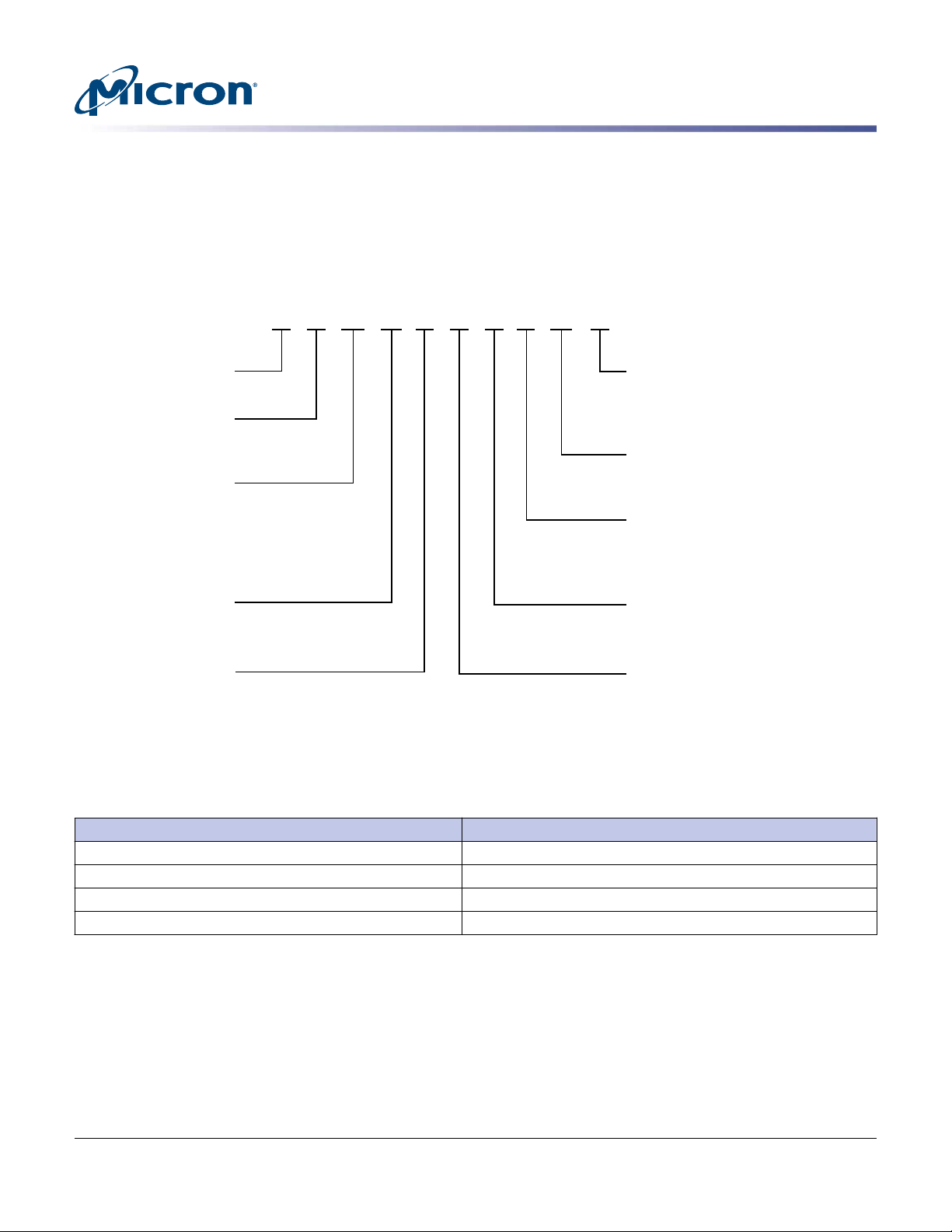
Micron Technology
Product Family
SD = Secure digital
Density
032 = 32GB
064 = 64GB
128 = 128GB
256 = 256GB
NAND Component
AH = TLC 256Gb, x8, 3.3V (3D)
Controller Revision
C6 = Revision C6
Production Status
Blank = Production
ES = Engineering samples
Custom Designator
Blank = Standard
Operating Temperature Range
WT = –25°C to +85°C
IT = –40°C to +85°C
Special Features
1 = First genaration
Packaging
RG = Full size SD
MS = microSD
MT SD 128 AH C6 MS-1 WT XX ES
Micron Confidential and Proprietary
Industrial microSDHC and microSDXC Card
Features
Part Number Ordering Information
Micron microSD memory cards are available in different configurations and densities. Verify valid part numbers
by using Micron’s part catalog search at www.micron.com. To compare features and specifications by device type,
visit www.micron.com/products. Contact the factory for cards not found.
Figure 1: Marketing Part Number Chart
Note:
1. Not all combinations are necessarily available. For a list of available devices or for further information on
any aspect of these products, please contact your nearest Micron sales office.
Table 1: Ordering Information
Part Number Capacity
MTSD032AHC6MS-1WT 32GB
MTSD064AHC6MS-1WT 64GB
MTSD128AHC6MS-1WT 128GB
MTSD256AHC6MS-1WT 256GB
CCM005-816717818-10492
Industrial_microSD_Card_32GB-256GB_AH.pdf - Rev. D 05/18 EN
2
Micron Technology, Inc. reserves the right to change products or specifications without notice.
© 2018 Micron Technology, Inc. All rights reserved.
Page 3

Micron Confidential and Proprietary
Industrial microSDHC and microSDXC Card
Important Notes and Warnings
Important Notes and Warnings
Micron Technology, Inc. ("Micron") reserves the right to make changes to information published in this document,
including without limitation specifications and product descriptions. This document supersedes and replaces all
information supplied prior to the publication hereof. You may not rely on any information set forth in this document if you obtain the product described herein from any unauthorized distributor or other source not authorized
by Micron.
Automotive Applications. Products are not designed or intended for use in automotive applications unless specifically designated by Micron as automotive-grade by their respective data sheets. Distributor and customer/distributor shall assume the sole risk and liability for and shall indemnify and hold Micron harmless against all claims,
costs, damages, and expenses and reasonable attorneys' fees arising out of, directly or indirectly, any claim of
product liability, personal injury, death, or property damage resulting directly or indirectly from any use of nonautomotive-grade products in automotive applications. Customer/distributor shall ensure that the terms and conditions of sale between customer/distributor and any customer of distributor/customer (1) state that Micron
products are not designed or intended for use in automotive applications unless specifically designated by Micron
as automotive-grade by their respective data sheets and (2) require such customer of distributor/customer to indemnify and hold Micron harmless against all claims, costs, damages, and expenses and reasonable attorneys'
fees arising out of, directly or indirectly, any claim of product liability, personal injury, death, or property damage
resulting from any use of non-automotive-grade products in automotive applications.
Critical Applications. Products are not authorized for use in applications in which failure of the Micron component could result, directly or indirectly in death, personal injury, or severe property or environmental damage
("Critical Applications"). Customer must protect against death, personal injury, and severe property and environmental damage by incorporating safety design measures into customer's applications to ensure that failure of the
Micron component will not result in such harms. Should customer or distributor purchase, use, or sell any Micron
component for any critical application, customer and distributor shall indemnify and hold harmless Micron and
its subsidiaries, subcontractors, and affiliates and the directors, officers, and employees of each against all claims,
costs, damages, and expenses and reasonable attorneys' fees arising out of, directly or indirectly, any claim of
product liability, personal injury, or death arising in any way out of such critical application, whether or not Micron or its subsidiaries, subcontractors, or affiliates were negligent in the design, manufacture, or warning of the
Micron product.
Customer Responsibility. Customers are responsible for the design, manufacture, and operation of their systems,
applications, and products using Micron products. ALL SEMICONDUCTOR PRODUCTS HAVE INHERENT FAILURE RATES AND LIMITED USEFUL LIVES. IT IS THE CUSTOMER'S SOLE RESPONSIBILITY TO DETERMINE
WHETHER THE MICRON PRODUCT IS SUITABLE AND FIT FOR THE CUSTOMER'S SYSTEM, APPLICATION, OR
PRODUCT. Customers must ensure that adequate design, manufacturing, and operating safeguards are included
in customer's applications and products to eliminate the risk that personal injury, death, or severe property or environmental damages will result from failure of any semiconductor component.
Limited Warranty. In no event shall Micron be liable for any indirect, incidental, punitive, special or consequential
damages (including without limitation lost profits, lost savings, business interruption, costs related to the removal
or replacement of any products or rework charges) whether or not such damages are based on tort, warranty,
breach of contract or other legal theory, unless explicitly stated in a written agreement executed by Micron's duly
authorized representative.
CCM005-816717818-10492
Industrial_microSD_Card_32GB-256GB_AH.pdf - Rev. D 05/18 EN
3
Micron Technology, Inc. reserves the right to change products or specifications without notice.
© 2018 Micron Technology, Inc. All rights reserved.
Page 4
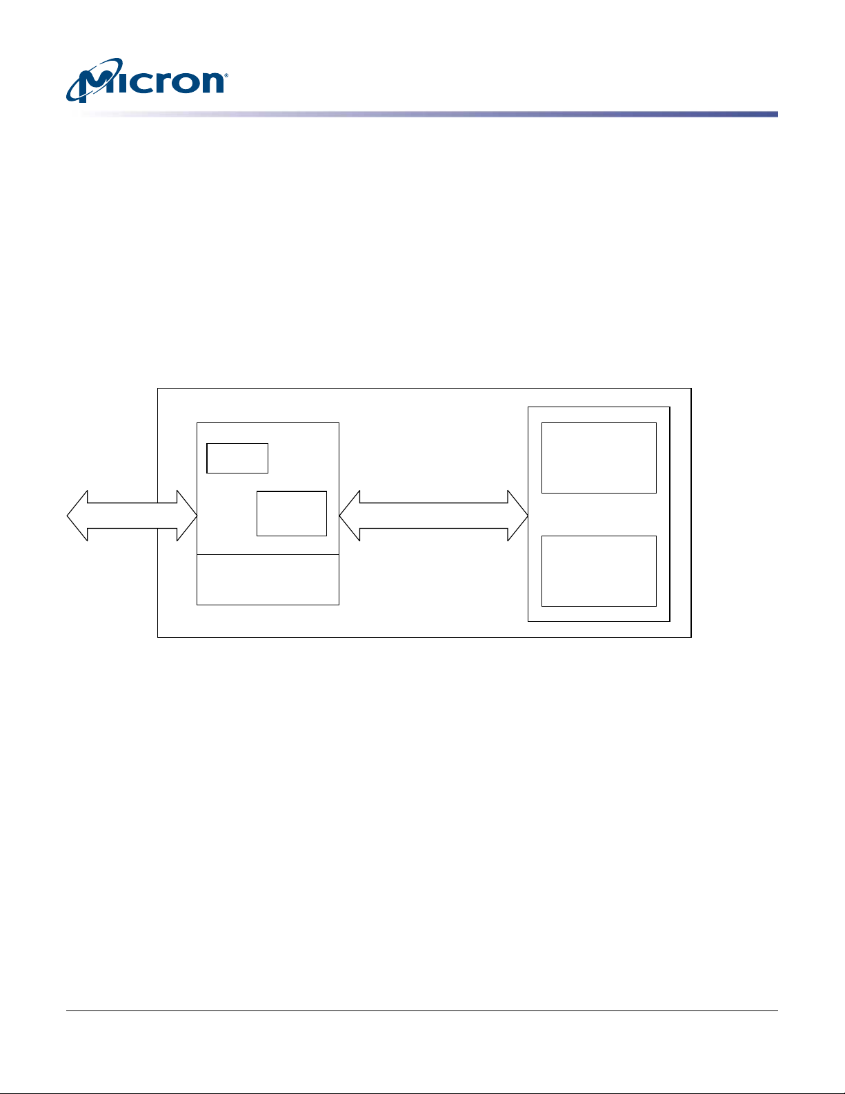
General Description
The microSD card is an advanced Micron® 3D NAND Flash memory technology based
removable storage device specifically designed to meet the performance, capacity, and
quality required for industrial devices or systems. In addition to mass storage-specific
Flash memory, the microSD card includes an on-board intelligent controller which
manages interface protocols, security algorithms for content protection, data storage
and retrieval, as well as error correction code (ECC) algorithms, defect handling, sudden
power-off safeguard and wear leveling.
The microSD card includes one or more NAND Flash memory components and a microSD card controller. The density of a card depends on the number of die within the
package and the density of each die.
Figure 2: Functional Block Diagram
Micron Confidential and Proprietary
Industrial microSDHC and microSDXC Card
General Description
SD protocol
CPU
Data buffer
Note:
Media
manager
1. Not drawn to scale.
NAND Flash interface
Micron
NAND Flash
Micron
NAND Flash
(optional)
CCM005-816717818-10492
Industrial_microSD_Card_32GB-256GB_AH.pdf - Rev. D 05/18 EN
4
Micron Technology, Inc. reserves the right to change products or specifications without notice.
© 2018 Micron Technology, Inc. All rights reserved.
Page 5
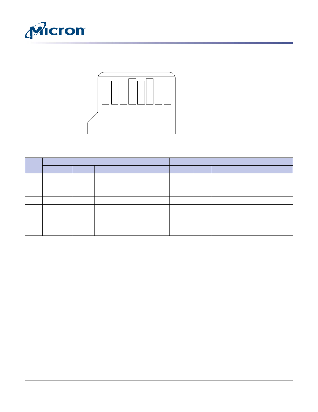
1 2 3
4 5 6 7
8
Micron Confidential and Proprietary
Industrial microSDHC and microSDXC Card
Pad Assignment and Descriptions
Figure 3: microSD Card Pad Assignment (Bottom View)
Table 2: MicroSD Contact Pad Description
Pad Assignment and Descriptions
Pad #
1 DAT2
Symbol Type1Description Symbol Type1Description
2
I/O/PP Data line [Bit 2] RSV – Reserved
2 CD/DAT32I/O/PP3Card detect/data line [Bit 3] CS I
SD Mode SPI Mode
3
Chip select (active low)
3 CMD PP Command/response DI I Data in
4 V
DD
S Supply voltage V
DD
S Supply voltage
5 CLK I Clock SCLK I Clock
6 V
SS
S Supply voltage ground V
SS
S Supply voltage ground
7 DAT0 I/O/PP Data line [Bit 0] DO O/PP Data out
8 DAT1
2
I/O/PP Data line [Bit 1] RSV – Reserved
Notes:
1. S: power supply; I: input; O: output using push-pull drivers; PP: I/O using push-pull drivers.
2. The extended DAT lines (DAT1-DAT3) are input on power-up. They start to operate as
DAT lines after SET_BUS_WIDTH (ACMD6) command. The host shall keep its own DAT1DAT3 lines in input mode, as well, while they are not used.
3. After power-up, pad 2 is configured as an input with an internal 50kΩ pull-up (for card
detection and SPI mode selection). The pull-up should be disconnected prior to regular
data transfer by issuing the SET_CLR_CARD_DETECT (ACMD42) command.
CCM005-816717818-10492
Industrial_microSD_Card_32GB-256GB_AH.pdf - Rev. D 05/18 EN
5
Micron Technology, Inc. reserves the right to change products or specifications without notice.
© 2018 Micron Technology, Inc. All rights reserved.
Page 6
Micron Confidential and Proprietary
Performance and Capacity
Performance
Using a striping method across multiple NAND Flash devices the card read and write
performance is optimized.
The Industrial microSD cards also use performance features of the underlying NAND
Flash to increase speed in streaming applications. By sending larger packets of sequential data, the Industrial microSD card can better utilize NAND Flash features to enhance
performance.
Table 3: Measured Performance (25°C, VDD = 3.3V)
Industrial microSDHC and microSDXC Card
Performance and Capacity
Density
1
Sequential Read
2
Sequential Write
2
32GB 90 MB/s 25 MB/s
64GB 90 MB/s 45 MB/s
128GB 90 MB/s 45 MB/s
256GB 90 MB/s 45 MB/s
Notes:
1. 1GB = 1 billion bytes.
2. Measurements are based on a 100MB file size in UHS-I mode and depend on the host
configuration used to run the test.
Capacity
When quoting device capacity, Micron uses the formatted capacity, not the raw number
of bytes available.
Table 4: Bytes Available After Factory Formatting (FAT32 for SDHC card and exFAT for SDXC card)
Density
1
Usable Bytes
2
Speed Class
3
32GB 29,884,416,000 Class10, U1 Class1 (A1)
64GB 59,760,443,392 Class10, U1 Class1 (A1)
128GB 124,688,269,312 Class10, U1 Class1 (A1)
256GB 249,376,538,624 Class10, U1 Class1 (A1)
Application Performance
3, 4
Class
Notes:
1. 1GB = 1 billion bytes.
2. Actual user usable capacity. When cloning disk partitions, the master disk should always
3. Class is determined by Testmetrix VTE4100 Compliance Test.
4. Enable users to run their smartphone apps from the installed memory card.
CCM005-816717818-10492
Industrial_microSD_Card_32GB-256GB_AH.pdf - Rev. D 05/18 EN
be formatted to no more than the minimum guaranteed usable bytes available for that
card capacity.
6
Micron Technology, Inc. reserves the right to change products or specifications without notice.
© 2018 Micron Technology, Inc. All rights reserved.
Page 7

OCR Register
The 32-bit operation conditions register defines the supported operating voltage ranges
for the power supply and supported access modes of the microSD card. Additionally,
this register includes status information bits.
Table 5: OCR Field Parameters
OCR-Slice OCR Value Description
[31] 1b (ready)/0b (busy) Card power-up status bit (busy)
[30] 1b Card Capacity Status (CCS)
[29:25] 0 0000b Reserved
[24] 1b (switching)/0b (maintained) Switching to 1.8V Accepted (S18A)
[23:15] 1 1111 1111b VDD: 2.7–3.6V range
[14:0] 000 0000 0000 0000b Reserved
Micron Confidential and Proprietary
Industrial microSDHC and microSDXC Card
OCR Register
1
2
Notes:
1. This bit is set to LOW if the card has not finished the power-up routine.
2. This bit is valid only when the card power-up status bit is set.
CCM005-816717818-10492
Industrial_microSD_Card_32GB-256GB_AH.pdf - Rev. D 05/18 EN
7
Micron Technology, Inc. reserves the right to change products or specifications without notice.
© 2018 Micron Technology, Inc. All rights reserved.
Page 8

Micron Confidential and Proprietary
Industrial microSDHC and microSDXC Card
CID Register
CID Register
The card identification (CID) register is 128 bits wide. It contains the device identification information used during the card identification phase as required by SD protocol.
Each card is created with a unique identification number.
Table 6: CID Register Field Parameters
Name Field Width CID-Slice CID Value
Manufacturer ID MID 8 [127:120] 09h
OEM/Application ID OID 16 [119:104] 41 50h
32GB: MB33A
Product name PNM 40 [103:64]
Product revision PRV 8 [63:56] –
Product serial number PSN 32 [55:24] –
Reserved – 4 [23:20] –
Manufacturing date MDT 12 [19:8] –
CRC7 checksum CRC 7 [7:1] –
Not used, always 1 – 1 [0] 1
64GB: MB43A
128GB: MB53A
256GB: MB63A
CCM005-816717818-10492
Industrial_microSD_Card_32GB-256GB_AH.pdf - Rev. D 05/18 EN
8
Micron Technology, Inc. reserves the right to change products or specifications without notice.
© 2018 Micron Technology, Inc. All rights reserved.
Page 9

Micron Confidential and Proprietary
CSD Register
The card-specific data (CSD) register provides information about accessing the card
contents. The CSD register defines the data format, error correction type, maximum data access time, as well as whether the DSR register can be used, and so forth. The programmable part of the register (entries marked with W in the following table) can be
changed by the PROGRAM_CSD (CMD27) command. The types of the entries in the table below are coded as follows: R = readable, W(1) = writable once, W = multiple writable.
Table 7: CSD Register Field Parameters
Industrial microSDHC and microSDXC Card
CSD Register
Name Field Width Cell Type CSD-Slice CSD Value
CSD structure CSD_STRUCTURE 2 R [127:126] 01b
Reserved – 6 R [125:120] 00 0000b
Data read access time TAAC 8 R [119:112] 0Eh
Data read access time in CLK cycles (NSAC × 100)
Maximum data transfer rate TRAN_SPEED 8 R [103:96] -
Card command classes CCC 12 R [95:84] 010110110101b
Maximum read data block
length
Partial blocks for read allowed READ_BL_PARTIAL 1 R [79:79] 0
Write block misalignment WRITE_BLK_MISALIGN 1 R [78:78] 0
Read block misalignment READ_BLK_MISALIGN 1 R [77:77] 0
DSR implemented DSR_IMP 1 R [76:76] 0
Reserved – 6 R [75:70] 00 0000b
Device size C_SIZE 22 R [69:48] 32GB - 0x00F0BF
Reserved – 1 R [47:47] 0
Erase single block enable ERASE_BLK_EN 1 R [46:46] 1
Erase sector size SECTOR_SIZE 7 R [45:39] 7Fh
Write protect group size WP_GRP_SIZE 7 R [38:32] 000 0000b
Write protect group enable WP_GRP_ENABLE 1 R [31:31] 0
Reserved – 2 R [30:29] 00b
Write speed factor R2W_FACTOR 3 R [28:26] 010b
Maximum write data block
length
Partial blocks for write allowed WRITE_BL_PARTIAL 1 R [21:21] 0
Reserved – 5 R [20:16] 0 0000b
File format group FILE_FORMAT_GRP 1 R [15:15] 0
Copy flag COPY 1 R/W(1) [14:14] 0
Permanent write protection PERM_WRITE_PROTECT 1 R/W(1) [13:13] 0
NSAC 8 R [111:104] 00h
READ_BL_LEN 4 R [83:80] 9
64GB - 0x01BD7F
128GB - 0x03A13F
256GB - 0x07427F
WRITE_BL_LEN 4 R [25:22] 9
1
CCM005-816717818-10492
Industrial_microSD_Card_32GB-256GB_AH.pdf - Rev. D 05/18 EN
9
Micron Technology, Inc. reserves the right to change products or specifications without notice.
© 2018 Micron Technology, Inc. All rights reserved.
Page 10

Micron Confidential and Proprietary
Industrial microSDHC and microSDXC Card
Table 7: CSD Register Field Parameters (Continued)
CSD Register
Name Field Width Cell Type CSD-Slice CSD Value
Temporary write protection TMP_WRITE_PROTECT 1 R/W [12:12] 0
File format FILE_FORMAT 2 R [11:10] 0
Reserved – 2 R [9:8] 00b
CRC CRC 7 R/W [7:1] xxxxxxxb
Not used, always 1 – 1 – [0:0] 1
Note:
1. All register table values reflect their expected state after card initialization and prior to
host issuing CMD6.
1
CCM005-816717818-10492
Industrial_microSD_Card_32GB-256GB_AH.pdf - Rev. D 05/18 EN
10
Micron Technology, Inc. reserves the right to change products or specifications without notice.
© 2018 Micron Technology, Inc. All rights reserved.
Page 11

Micron Confidential and Proprietary
Industrial microSDHC and microSDXC Card
SCR Register
SCR Register
In addition to the CSD register, there is another configuration register named SD card
configuration register (SCR). SCR provides information on the SD Memory Card's special features that were configured into the given card. The size of SCR register is 64 bits.
The types of all bits of SCR are R = readable.
Table 8: CSD Register Field Parameters
Cell
Description Field Width
SCR structure SCR_STRUCTURE 4 R [63:60] 0000b
SD memory card – Specification
version
Data status after erases DATA_STAT_AFTER_ERASE 1 R [55:55] 0
CPRM security support SD_SECURITY 3 R [54:52] 100b
DAT bus widths supported SD_BUS_WIDTHS 4 R [51:48] 0101b
Specification version 3.00 or later SD_SPEC3 1 R [47:47] 1b
Extended security support EX_SECURITY 4 R [46:43] 0000b
Specification version 4.00 or later SD_SPEC4 1 R [42:42] 0
Specification version 5.00 or later SD_SPECX 4 R [41:38] 0001b
Reserved – 2 R [37:36] 0
Command support bits CMD_SUPPORT 4 R [35:32] 0011b
Reserved for manufacturer usage – 32 R [31:0] 01 00 00 00h
SD_SPEC 4 R [59:56] 0010b
Type CSD-Slice CSD Value
CCM005-816717818-10492
Industrial_microSD_Card_32GB-256GB_AH.pdf - Rev. D 05/18 EN
11
Micron Technology, Inc. reserves the right to change products or specifications without notice.
© 2018 Micron Technology, Inc. All rights reserved.
Page 12

Micron Confidential and Proprietary
Industrial microSDHC and microSDXC Card
Command Set
Command Set
The SD specification categorizes commands into classes. Table 9 shows commands
supported by the industrial microSD card.
Table 9: Supported Commands
Card Command
Command Type
Basic commands Class 0 CMD0, CMD2, CMD3, CMD7, CMD8, CMD9, CMD10, CMD11,
Block-oriented read commands Class 2 CMD16, CMD17, CMD18, CMD19, CMD20, CMD23
Block-oriented write commands Class 4 CMD16, CMD20, CMD23, CMD24, CMD25, CMD27
Erase commands Class 5 CMD32, CMD33, CMD38
Lock card Class 7 CMD16, CMD42
Application-specific commands
1
Switch commands Class 10 CMD6
Class (CCC) Supported Commands
CMD12, CMD13, CMD15
Class 8 CMD55, CMD56, ACMD6, ACMD13, ACMD182, ACMD22,
ACMD23, ACMD252, ACMD262, ACMD382, ACMD41, ACMD42,
ACMD432, ACMD442, ACMD442, ACMD452, ACMD462, ACMD472,
ACMD482, ACMD492, ACMD51
Notes:
1. Each application-specific (ACMD) command is a 2-sequence command. First, a CMD55 is
sent, followed by a CMDx, where x is the ACMDx value.
2. Refer to SD Specifications, Part 3, Security Specification, version 3.00 for a detailed explanation about the SD Security Features.
CCM005-816717818-10492
Industrial_microSD_Card_32GB-256GB_AH.pdf - Rev. D 05/18 EN
12
Micron Technology, Inc. reserves the right to change products or specifications without notice.
© 2018 Micron Technology, Inc. All rights reserved.
Page 13

Micron Confidential and Proprietary
Industrial microSDHC and microSDXC Card
Electrical Specifications
Electrical Specifications
Absolute Ratings and Operating Conditions
Stresses greater than those listed in Table 10 may cause permanent damage to the device. This is a stress rating only, and functional operation of the device at these or any
other conditions outside those indicated in the operational sections of this specification
is not implied. Exposure to absolute maximum rating conditions for extended periods
may adversely affect reliability.
Table 10: Absolute Maximum Ratings
Parameter/Condition Min Max Unit
VDD supply voltage 2.7 3.6 V
Storage temperature –40 +85 °C
Table 11: Recommended Operating Conditions
Parameter/Condition Symbol Min Typ Max Unit
Operating temperature T
Supply voltage V
Regulator supply voltage for 1.8V signaling V
Ground supply voltage V
A
DD
DDIO
SS
–25 – +85 °C
2.7 3.3 3.6 V
1.7 1.8 1.95 V
0 0 0 V
DC Characteristics
Table 12: DC Voltage Characteristics for 3.3V signaling
Parameter Symbol Min Max Unit Comments
Input low voltage V
Input high voltage V
Output low voltage V
Output high voltage V
IL
IH
OL
OH
Table 13: DC Voltage Characteristics for 1.8V signaling
Parameter Symbol Min
Input low voltage V
Input high voltage V
Output low voltage V
Output high voltage V
IL
IH
OL
OH
Vss - 0.30 0.25 × V
0.625 × V
DD
VDD + 0.30 V
– 0.125 × V
0.75 × V
DD
1
Max
DD
DD
– V IOH = –2mA @ VDD (MIN)
1
V
V IOL = 2mA @ VDD (MIN)
Unit Comments
Vss - 0.30 0.58 V
1.27 2.00 V
– 0.45 V IOL = 2mA
1.40 – V IOH = –2mA
Note:
CCM005-816717818-10492
Industrial_microSD_Card_32GB-256GB_AH.pdf - Rev. D 05/18 EN
1. As signaling level is generated by regulator in host and card, some of the values are defined by fixed value rather than based on VDD.
13
Micron Technology, Inc. reserves the right to change products or specifications without notice.
© 2018 Micron Technology, Inc. All rights reserved.
Page 14

AC Characteristics
Timing specifications including clock timing, input and output timings for all bus
modes are defined in SD Specifications. Refer to Section 6.6 and 6.7 of Part 1, Physical
Layer Specification, version 5.10 for detail information.
Electrostatic Discharge (ESD)
Contacts pads:
• Human body model of ±4kV according to IEC61000-4-2.
Non contacts pad area:
• Coupling plane discharge of ±8kV.
• Air discharge of ±15kV.
• Human body model according to IEC61000-4-2.
Micron Confidential and Proprietary
Industrial microSDHC and microSDXC Card
Electrical Specifications
CCM005-816717818-10492
Industrial_microSD_Card_32GB-256GB_AH.pdf - Rev. D 05/18 EN
14
Micron Technology, Inc. reserves the right to change products or specifications without notice.
© 2018 Micron Technology, Inc. All rights reserved.
Page 15

TBD
TBD
8.50 MAX
0.90 MIN
1.0
0.70 ±0.1
9.70
11.0
15.0
Micron Confidential and Proprietary
Package Dimensions
Figure 4 provides the physical dimensions of Micron microSD card. For detail dimensions and tolerances, refer to SDA microSD Card Addendum, Section 3.0 Mechanical
Specification for microSD Memory Card.
Figure 4: microSD Card – 11mm × 15mm
Industrial microSDHC and microSDXC Card
Package Dimensions
Note:
1. Dimensions are in millimeters.
Table 14: Package Specifications
Parameter Descriptions
Surface Plain (except contact area)
Edges Smooth edges
Weight 0.25gm
CCM005-816717818-10492
Industrial_microSD_Card_32GB-256GB_AH.pdf - Rev. D 05/18 EN
15
Micron Technology, Inc. reserves the right to change products or specifications without notice.
© 2018 Micron Technology, Inc. All rights reserved.
Page 16

Compliance
Micron Confidential and Proprietary
Industrial microSDHC and microSDXC Card
Compliance
Micron microSD card comply with the following:
• Micron Green Standard
• CE (Europe): EN 55032 Class B, RoHS
• FCC: CFR Title 47, Part 15 Class B
• BSMI (Taiwan): approval to CNS 13438 Class B and CNS 15663
• KC RRA (Korea): approval to KN32 Class B, KN 35 Class B
FCC Rules
R-REM-MU2-MTSDXXXAHC6MS
• W.E.E.E.: compliance with EU WEEE directive 2012/19/EC. Additional obligations
may apply to customers who place these products in the markets where WEEE is enforced.
• VCCI (Japan): 2015-04 Class B
• IC (Canada): ICES-003 Class B
- This Class B digital apparatus complies with Canadian ICES-003.
- Cet appareil numérique de la classe B est conforme à la norme NMB-003 du Canada.
- CAN ICES-3 (B)/NMB-3(B).
This equipment has been tested and found to comply with the limits for a Class B digital
device, pursuant to part 15 of the FCC Rules. These limits are designed to provide reasonable protection against harmful interference in a residential installation. This equipment generates, uses, and can radiate radio frequency energy and, if not installed and
used in accordance with the instructions, may cause harmful interference to radio communications. However, there is no guarantee that interference will not occur in a particular installation. If this equipment does cause harmful interference to radio or television reception, which can be determined by turning the equipment off and on, the user
is encouraged to try to correct the interference by one or more of the following measures:
• Reorient or relocate the receiving antenna.
CCM005-816717818-10492
Industrial_microSD_Card_32GB-256GB_AH.pdf - Rev. D 05/18 EN
16
Micron Technology, Inc. reserves the right to change products or specifications without notice.
© 2018 Micron Technology, Inc. All rights reserved.
Page 17

Micron Confidential and Proprietary
Industrial microSDHC and microSDXC Card
Compliance
• Increase the separation between the equipment and the receiver.
• Connect the equipment into an outlet on a circuit different from that to which the receiver is connected.
• Consult the dealer or an experienced radio/TV technician for help.
CCM005-816717818-10492
Industrial_microSD_Card_32GB-256GB_AH.pdf - Rev. D 05/18 EN
17
Micron Technology, Inc. reserves the right to change products or specifications without notice.
© 2018 Micron Technology, Inc. All rights reserved.
Page 18

Revision History
Rev. D – 05/18
Rev. C – 05/18
Rev. B – 02/18
Rev. A – 01/18
Micron Confidential and Proprietary
Industrial microSDHC and microSDXC Card
Revision History
• Update Compliance section for Canada and Taiwan
• Updated legal status to Production
• Added MTSD032AHC6MS-1WT (32GB) and MTSD064AHC6MS-1WT (64GB)
• Added Endurance: Total bytes written (TBW) values
• Updated Product name (PNM) in CID Register Field Parameters table
• Added Compliance section
• Updated the endurance for 128GB
• Preliminary version
8000 S. Federal Way, P.O. Box 6, Boise, ID 83707-0006, Tel: 208-368-4000
www.micron.com/products/support Sales inquiries: 800-932-4992
Micron and the Micron logo are trademarks of Micron Technology, Inc.
All other trademarks are the property of their respective owners.
This data sheet contains minimum and maximum limits specified over the power supply and temperature range set forth herein.
Although considered final, these specifications are subject to change, as further product development and data characterization some-
times occur.
CCM005-816717818-10492
Industrial_microSD_Card_32GB-256GB_AH.pdf - Rev. D 05/18 EN
18
Micron Technology, Inc. reserves the right to change products or specifications without notice.
© 2018 Micron Technology, Inc. All rights reserved.
 Loading...