

Micron MTFDJAK400MBS, MTFDJAK400MBT, MTFDJAK800MBS, MTFDJAK800MBT, MTFDJAL1T6MBS User Manual
...Page 1
Preliminary
S600DC Series 2.5-Inch SAS NAND Flash SSD
Features
S600DC Series 2.5-Inch SAS NAND Flash
SSD
MTFDJAK400MBS, MTFDJAK400MBT, MTFDJAK800MBS,
MTFDJAK800MBT, MTFDJAL1T6MBS, MTFDJAL1T6MBT,
MTFDJAL3T2MBS, MTFDJAL3T2MBT, MTFDJAK480MBT,
MTFDJAK960MBT, MTFDJAL1T9MBT, MTFDJAL3T8MBT,
MTFDJAL1T9MBU, MTFDJAL3T8MBU, MTFDJAK200MBW,
MTFDJAK400MBW
‡
Features
• Four endurance levels
– S655DC = 25 DWPD; S650DC = 10 DWPD
– S630DC = 2–3 DWPD; S610DC = <1 DWPD
• Micron® 16nm MLC NAND Flash
• RoHS-compliant package
• SAS
– Interface = 12 Gb/s
– Speed = 3 Gb/s, 6 Gb/s, 12 Gb/s, and auto-speed
negotiation
– SAS-3 support
• SAM-5 compliant
• Enterprise sector size support = 512, 520, 524, 528,
4096, 4160, 4192, and 4224-byte
• Hot-plug capable
• 128-entry command queue depth
• Digitally signed firmware for SED and non-SED
• FIPS140-2 level 2 certification option available on
each S650DC 2.5-inch device:
400GB, 800GB, 1600GB, and 3200GB
• Secure erase via format unit
• Reliability
– MTTF: 2.5 million device hours
– Static and dynamic wear leveling
– Uncorrectable bit error rate (UBER): 1 × 1017 bits
transferred
• Capacity 2 (unformatted): 200GB, 400GB, 480GB,
800GB, 960GB, 1600GB, 1920GB, 3200GB, 3840GB
• Endurance: TBW over warranty period
– S655DC (25 DWPD):
200GB-8PB, 400GB-17PB
– S650DC (10 DWPD):
400GB-7PB, 800GB-14PB
1600GB-29PB, 3200GB-58PB
1
4
• Endurance: TBW over warranty period
– S630DC (2–3 DWPD):
400GB-2.1PB, 480GB-2.6PB,
800GB-2.9PB, 960GB-5.2PB,
1600GB-5.8PB, 1920GB-10PB,
3200GB-12PB, 3840-21PB
– S610DC (1 DWPD):
1920GB-2.8PB, 3840GB-5.6PB
• Electrical
– Supply voltage: 5 VDC (±5%) and 12 VDC (±5%)
• Mechanical
– 2.5-inch drive: 100.5mm × 69.85mm × 7mm, and
100.5mm × 69.85mm × 15mm
• Field-upgradeable firmware
• Power consumption: 9W (TYP) and 12W (MAX)
– Configurable through information exceptions
mode page
• Operating temperature
– 0°C to +50°C (MAX)
Notes:
Warranty: Contact your Micron sales representative
for further information regarding the product, including product warranties.
1. Product achieves a mean time to failure
(MTTF) based on population statistics that
are not relevant to individual units.
2. 1GB = 1 billion bytes; formatted capacity is
less.
3. Based on ambient air temperature.
4. Total bytes written (TBW): Warranty defined in the product manual is five years or
device expiration as indicated by the device
life indicator, whichever comes first.
3
4
PDF: 09005aef8642dd23
s600dc_series_2_5_sas_ssd.pdf - Rev. F 3/16 EN
‡Products and specifications discussed herein are for evaluation and reference purposes only and are subject to change by
Micron without notice. Products are only warranted by Micron to meet Micron’s production data sheet specifications.
1
Micron Technology, Inc. reserves the right to change products or specifications without notice.
© 2015 Micron Technology, Inc. All rights reserved.
Page 2
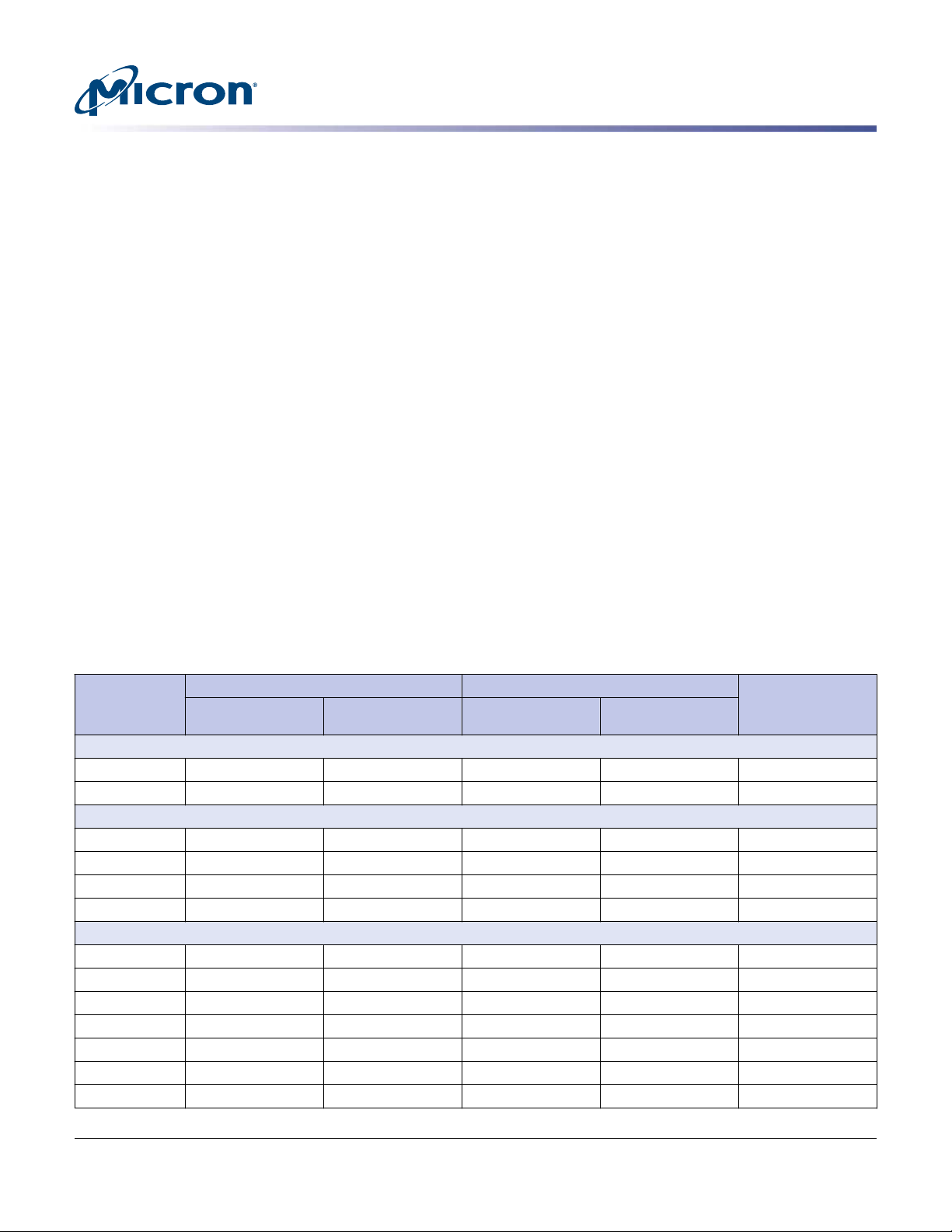
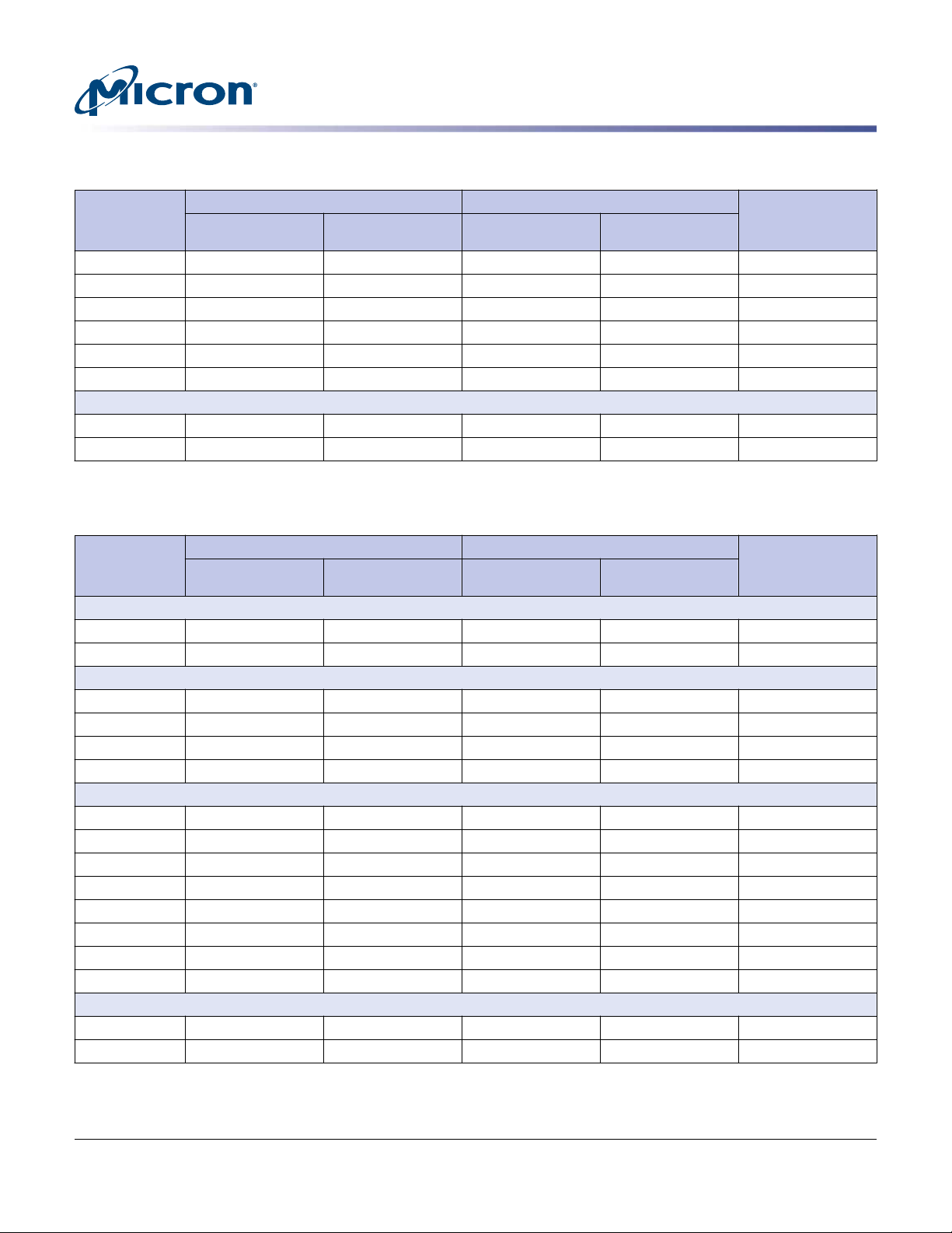
S600DC Series 2.5-Inch SAS NAND Flash SSD
Table 1: Performance
Notes apply to entire table
Sequential
Device
and
Capacity
128KB Transfer
Read
(MB/s)
Write
(MB/s)
(KIOPS)
S655DC
200GB 1550 600 200 120 85 115
400GB 1700 850 200 120 115 115
S650DC
400GB 1550 625 180 67 80 115
800GB 1850 850 200 80 105 115
1600GB 1900 850 200 80 120 115
3200GB 1900 800 200 80 120 115
S630DC
400GB 1400 490 180 20 45 115
480GB 1550 615 180 30 45 115
800GB 1400 710 180 20 45 115
960GB 1700 850 180 30 65 115
1600GB 1600 850 180 20 45 115
1920GB 1850 850 180 30 65 115
3200GB 1600 850 180 20 45 115
3840GB 1850 770 180 30 65 115
S610DC
1920GB 1700 850 190 12 45 115
3840GB 1600 770 190 15 45 115
Random
4KB Transfer
Read
Write
(KIOPS)
Random
4KB Transfer (70/30)
Mixed Read/Write
(KIOPS)
Latency (µs)
Preliminary
Features
Average
Notes:
1. Typical I/O performance numbers: measured using an iometer in a steady state region with a queue depth of
32 for sequential and random transfers and write cache enabled; a queue depth of 1 for READ/WRITE latency values.
2. Consistent host system interface, configurations, and variables: maintained with variation only in the drive
being tested.
3. Response time measurement conditions: recorded with nominal power at 25 °C ambient temperature.
4. Page-to-page response times: derived from all possible page-to-page accesses on a sequentially preconditioned drive.
5. Average response time: derived from at least 5000 access measurements between programmable pages on a
randomly preconditioned drive to ensure a true statistical random average.
PDF: 09005aef8642dd23
s600dc_series_2_5_sas_ssd.pdf - Rev. F 3/16 EN
2
Micron Technology, Inc. reserves the right to change products or specifications without notice.
© 2015 Micron Technology, Inc. All rights reserved.
Page 3
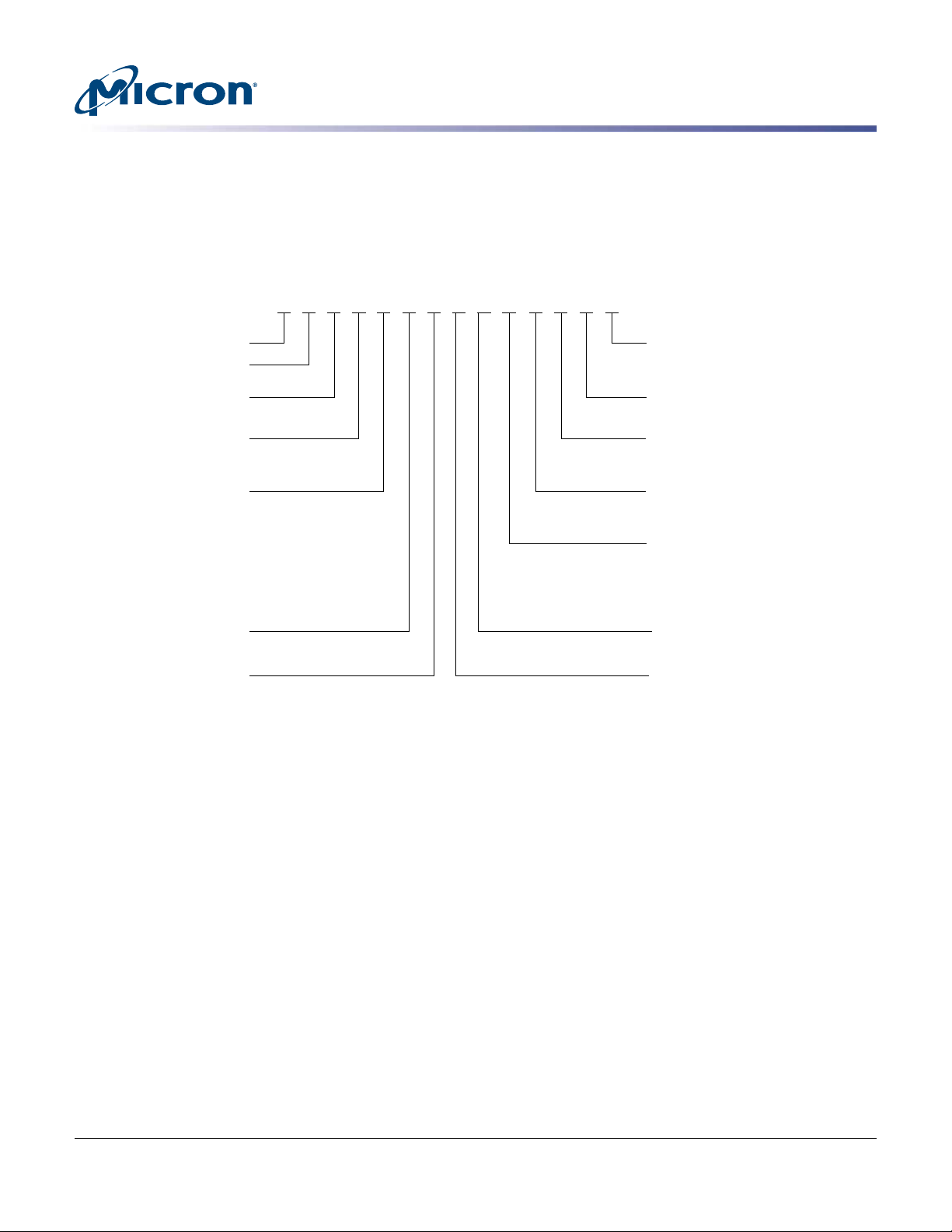
MT FD J AK 400 M BS - 1 AN 1 ES
Micron Technology
Product Family
FD = Flash drive
Drive Interface
J = SAS 12.0 Gb/s
Drive Form Factor
AK = 2.5-inch (7mm)
AL = 2.5-inch (15mm)
Drive Density
200 = 200GB
400 = 400GB
480 = 480GB
800 = 800GB
960 = 960GB
1T6 = 1600GB (1.6TB)
1T9 = 1920GB (1.92TB)
3T2 = 3200GB (3.2TB)
3T8 = 3840GB (3.84TB)
NAND Flash Type
M = MLC
Product Family
BS = S650DC
BT = S630DC
BU = S610DC
BW = S655DC
Production Status
Blank = Production
ES = Engineering sample
Customer Designator
YY = Standard
Hardware Feature
AB = Standard
FC = FIPS140-2 Level 2
Extended Firmware Features
Z = None
6 = SED-TCG eSSC
Sector Size
1 = 512 byte
2 = 520 byte
3 = 528 byte
NAND Flash Component
AN = L95B, 128Gb, MLC, 3.3V
BOM Revision
1 = 1st generation
2 = 2nd generation
Z AB YY
Preliminary
S600DC Series 2.5-Inch SAS NAND Flash SSD
Features
Part Numbering Information
Micron’s 600 series SAS SSD is available in different configurations and densities. Visit www.micron.com for a list
of valid part numbers.
Figure 1: Part Number Chart
PDF: 09005aef8642dd23
s600dc_series_2_5_sas_ssd.pdf - Rev. F 3/16 EN
3
Micron Technology, Inc. reserves the right to change products or specifications without notice.
© 2015 Micron Technology, Inc. All rights reserved.
Page 4
Micron 16nm
eMLC NAND
Controller SoC
Phy
Mgmt
MO
offload
MO
offload
MO
offload
Interface
R5
processor
F.T.L.
R5
processor
x9
Flash ctlr PSM
Flash ctlr PSM
Flash ctlr PSM
Flash ctlr PSM
Flash ctlr PSM
Flash ctlr PSM
Flash ctlr PSM
Flash ctlr PSM
Flash ctlr PSM
Controller SoC
Phy
Mgmt
MO
offload
MO
offload
MO
offload
Interface
R5
processor
F.T.L.
R5
processor
x9
NAND bridge controller
PSM
Data path
Micron 16nm
eMLC NAND
Micron 16nm
eMLC NAND
Channel 1
Channel 2
Flash ctlr PSM
Flash ctlr PSM
Flash ctlr PSM
Flash ctlr PSM
Flash ctlr PSM
Flash ctlr PSM
Flash ctlr PSM
Flash ctlr PSM
Flash ctlr PSM
ONFI target
S600DC Series 2.5-Inch SAS NAND Flash SSD
General Description
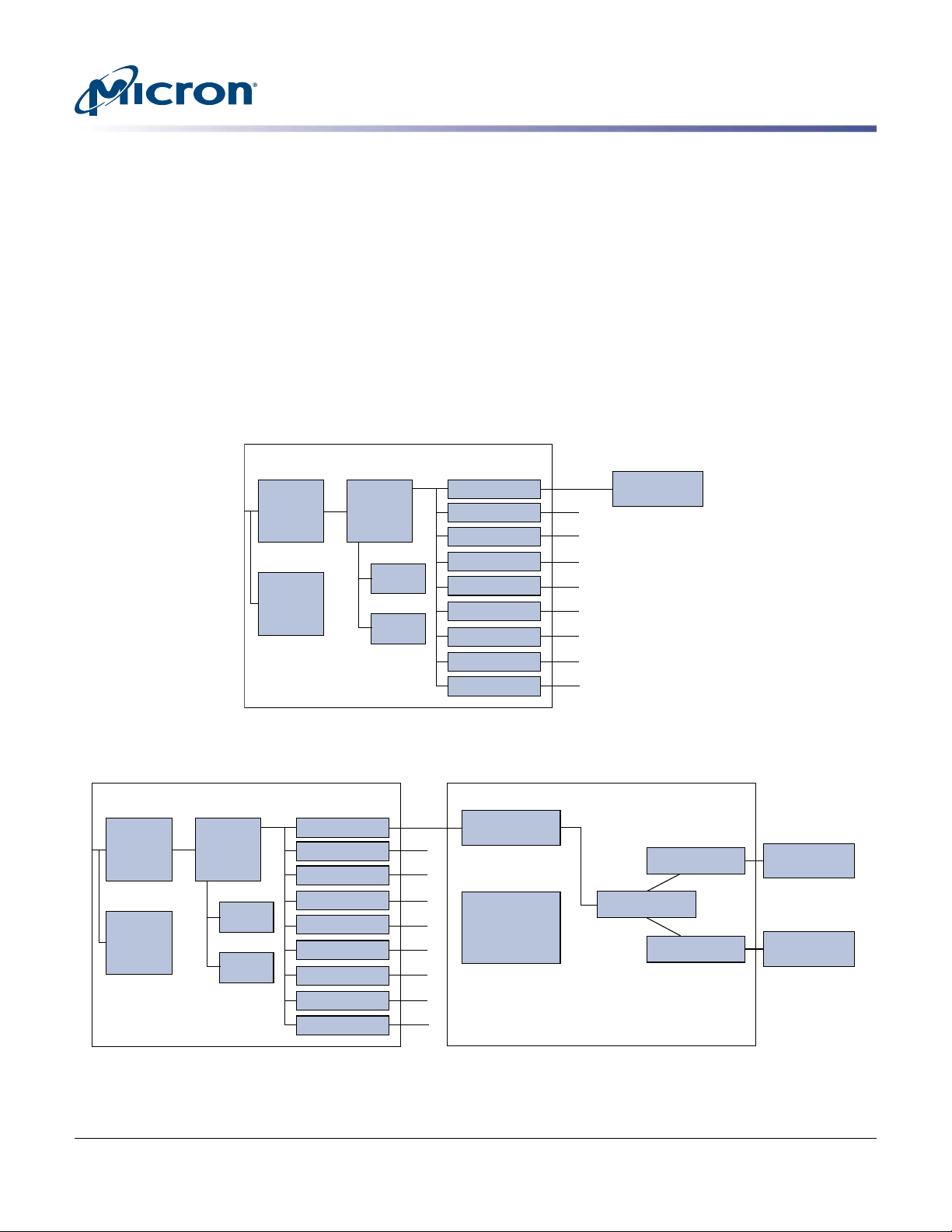
General Description
Micron’s solid state drive (SSD) uses a single-chip controller with a dual-port SAS interface on the system side and 10 channels of Micron NAND Flash internally. Packaged in
an HDD replacement enclosure, the SSD integrates easily into existing storage infrastructures.
The SSD is designed to support and manage the needs of highly available, high-performance platforms that use significant read/write mixed workloads. Optimized to support enterprise needs previously supported only by single-level cell (SLC) solutions, this
SSD provides endurance and data integrity required by growing environments.
Functional Block Diagrams
Figure 2: Functional Block Diagram – 7mm Variant (Controller Attached to NAND Directly)
Preliminary
Figure 3: Functional Block Diagram – 15mm Variant (Controller Attached to NAND by Bridge)
PDF: 09005aef8642dd23
s600dc_series_2_5_sas_ssd.pdf - Rev. F 3/16 EN
4
Micron Technology, Inc. reserves the right to change products or specifications without notice.
© 2015 Micron Technology, Inc. All rights reserved.
Page 5
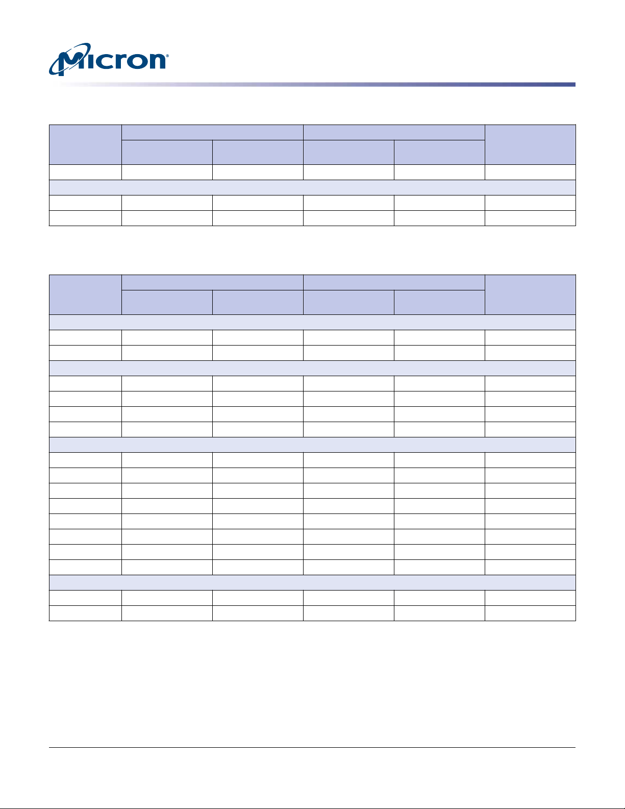
S600DC Series 2.5-Inch SAS NAND Flash SSD
Logical Block Address Configuration
Each device is set to report its logical block address (LBA) settings, which ensure sufficient storage per device capacity. The tables below show LBA settings according to device size.
Standard OEM models are formatted to 512 bytes per block. The block size is selectable
at format time, and users with the necessary equipment can modify the data block size
to capacities different than those listed below before issuing a format command. To
provide a stable target capacity environment while also providing users with flexibility,
Micron recommends product planning.
Micron ensures that current and future product generations will meet capacity points at
certain block sizes. Planning with this in mind ensures a stable operating point with
backward and forward compatibility across product generations. The current operating
points for each device are shown below. The capacity stated is identical when the drive
is formatted with or without PI enabled.
Programmable Drive Capacity
Preliminary
Logical Block Address Configuration
Using the MODE SELECT command, users can change the drive capacity to less than its
maximum value. A value of zero in the Number of Blocks field means that the MODE
SELECT command will leave the drive capacity unchanged. A value greater than zero
and less than the maximum number of LBAs in the Number of Blocks field means that
the MODE SELECT command will change the drive capacity to the value in the Number
of Blocks field. A value greater than the maximum number of LBAs means that the
MODE SELECT command will round down to the maximum capacity.
Table 2: Standard LBA Settings – 512-Byte Sector Size
Total LBA Max LBA User Available
Device and
Capacity
S655DC
200GB 390,721,968 1749F1B0 390,721,967 1749F1AF 200,049,647,616
400GB 781,422,768 2E9390B0 781,422,767 2E9390AF 400,088,457,216
S650DC
400GB 781,422,768 2E9390B0 781,422,767 2E9390AF 400,088,457,216
800GB 1,562,824,368 5D26CEB0 1,562,824,367 5D26CEAF 800,166,076,416
1600GB 3,125,627,568 BA4D4AB0 3,125,627,567 BA4D4AAF 1,600,321,314,816
3200GB 6,251,233,968 1749A42B0 6,251,233,967 1749A42AF 3,200,631,791,616
S630DC
400GB 781,422,768 2E9390B0 781,422,767 2E9390AF 400,088,457,216
480GB 937,703,088 37E436B0 937,703,087 37E436AF 480,103,981,056
800GB 1,562,824,368 5D26CEB0 1,562,824,367 5D26CEAF 800,166,076,416
960GB 1,875,385,008 6FC81AB0 1,875,385,007 6FC81AAF 960,197,124,096
1600GB 3,125,627,568 BA4D4AB0 3,125,627,567 BA4D4AAF 1,600,321,314,816
1920GB 3,750,748,848 DF8FE2B0 3,750,748,847 DF8FE2AF 1,920,383,410,176
3200GB 6,251,233,968 1749A42B0 6,251,233,967 1749A42AF 3,200,631,791,616
Bytes
(Unformatted)Decimal Hexidecimal Decimal Hexidecimal
PDF: 09005aef8642dd23
s600dc_series_2_5_sas_ssd.pdf - Rev. F 3/16 EN
5
Micron Technology, Inc. reserves the right to change products or specifications without notice.
© 2015 Micron Technology, Inc. All rights reserved.
Page 6
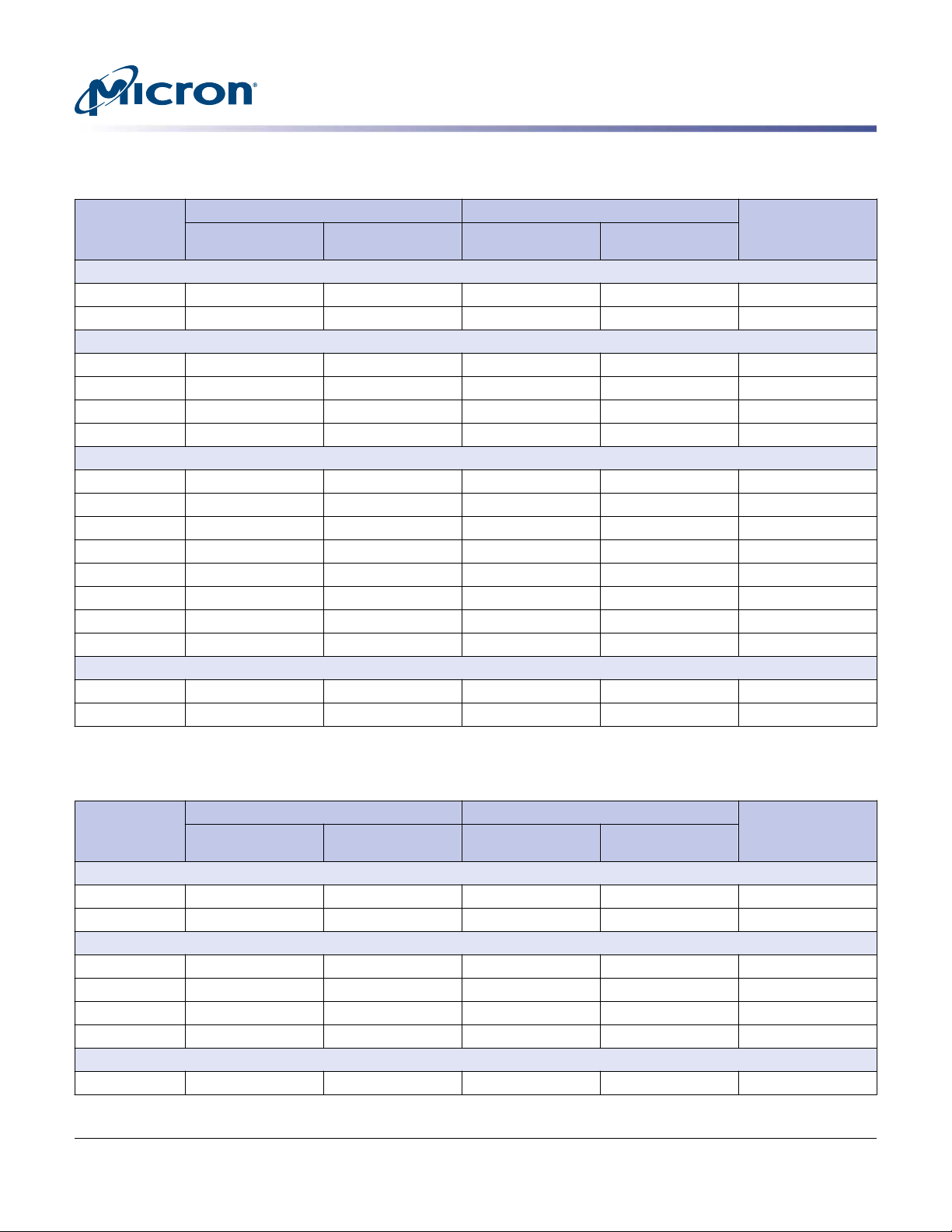
S600DC Series 2.5-Inch SAS NAND Flash SSD
Logical Block Address Configuration
Table 2: Standard LBA Settings – 512-Byte Sector Size (Continued)
Total LBA Max LBA User Available
Device and
Capacity
3840GB 7,501,476,528 1BF1F72B0 7,501,476,527 1BF1F72AF 3,840,755,982,336
S610DC
1920GB 3,750,748,848 DF8FE2B0 3,750,748,847 DF8FE2AF 1,920,383,410,176
3840GB 7,501,476,528 1BF1F72B0 7,501,476,527 1BF1F72AF 3,840,755,982,336
Table 3: Standard LBA Settings – 520-Byte Sector Size
Total LBA Max LBA User Available
Device and
Capacity
S655DC
200GB 382,435,904 16CB8240 382,435,903 16CB823F 198,866,670,080
400GB 764,871,800 2D970478 764,871,799 2D970477 397,733,336,000
S650DC
400GB 764,871,800 2D970478 764,871,799 2D970477 397,733,336,000
800GB 1,529,743,600 5B2E08F0 1,529,743,599 5B2E08EF 795,466,672,000
1600GB 3,059,487,192 B65C11D8 3,059,487,191 B65C11D7 1,590,933,339,840
3200GB 6,118,974,384 16CB823B0 6,118,974,383 16CB823AF 3,181,866,679,680
S630DC
400GB 764,871,800 2D970478 764,871,799 2D970477 397,733,336,000
480GB 917,846,160 36B53890 917,846,159 36B5388F 477,280,003,200
800GB 1,529,743,600 5B2E08F0 1,529,743,599 5B2E08EF 795,466,672,000
960GB 1,835,692,320 6D6A7120 1,835,692,319 6D6A711F 954,560,006,400
1600GB 3,059,487,192 B65C11D8 3,059,487,191 B65C11D7 1,590,933,339,840
1920GB 3,671,384,640 DAD4E240 3,671,384,639 DAD4E23F 1,909,120,012,800
3200GB 6,118,974,384 16CB823B0 6,118,974,383 16CB823AF 3,181,866,679,680
3840GB 7,342,769,280 1B5A9C480 7,342,769,279 1B5A9C47F 3,818,240,025,600
S610DC
1920GB 3,671,384,640 DAD4E240 3,671,384,639 DAD4E23F 1,909,120,012,800
3840GB 7,342,769,280 1B5A9C480 7,342,769,279 1B5A9C47F 3,818,240,025,600
Bytes
(Unformatted)Decimal Hexidecimal Decimal Hexidecimal
Bytes
(Unformatted)Decimal Hexidecimal Decimal Hexidecimal
Preliminary
PDF: 09005aef8642dd23
s600dc_series_2_5_sas_ssd.pdf - Rev. F 3/16 EN
6
Micron Technology, Inc. reserves the right to change products or specifications without notice.
© 2015 Micron Technology, Inc. All rights reserved.
Page 7
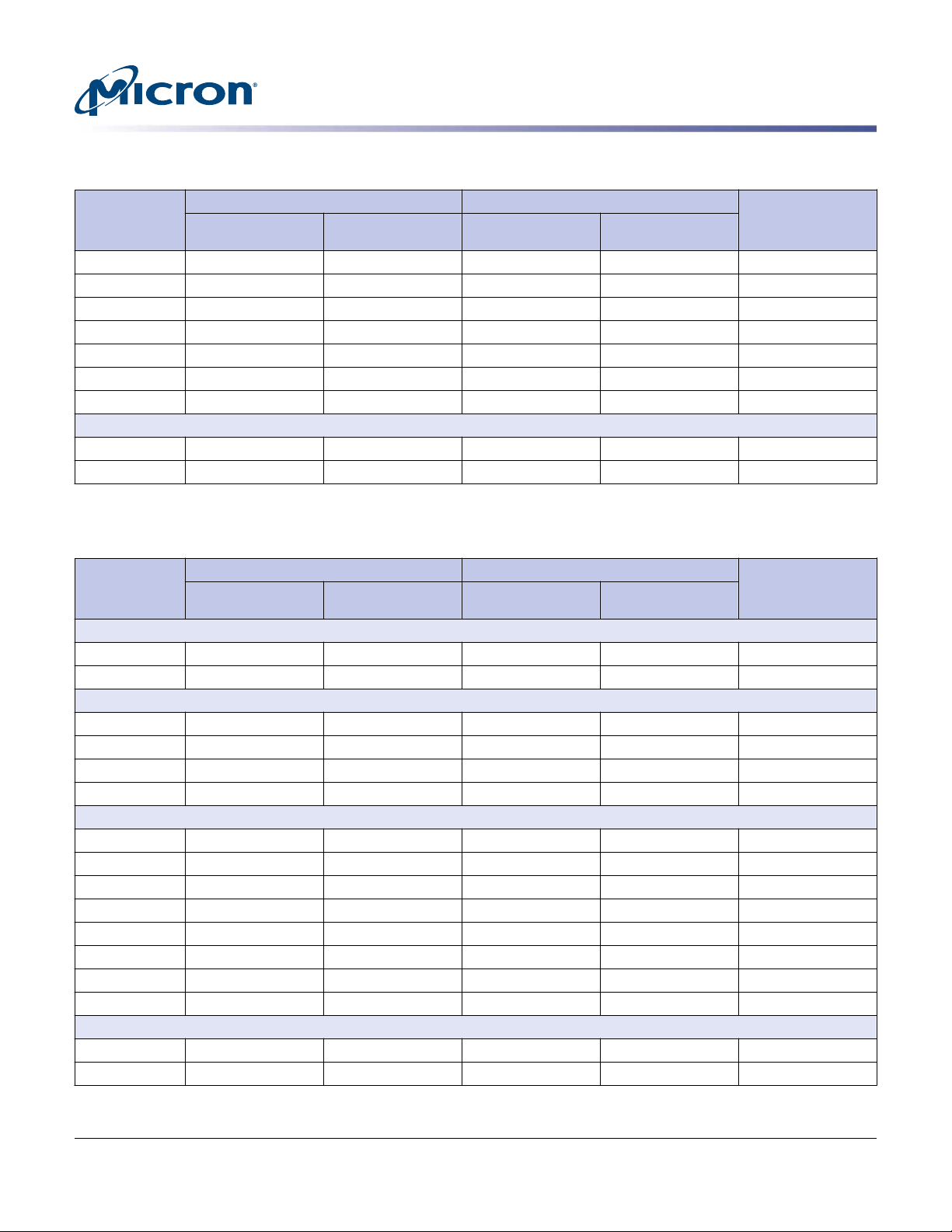
S600DC Series 2.5-Inch SAS NAND Flash SSD
Logical Block Address Configuration
Table 4: Standard LBA Settings – 524-Byte Sector Size
Total LBA Max LBA User Available
Device and
Capacity
S655DC
200GB 377,338,536 167DBAA8 377,338,535 167DBAA7 197,725,392,864
400GB 754,677,072 2CFB7550 754,677,071 2CFB754F 395,450,785,728
S650DC
400GB 754,677,072 2CFB7550 754,677,071 2CFB754F 395,450,785,728
800GB 1,509,354,136 59F6EA98 1,509,354,135 59F6EA97 790,901,567,264
1600GB 3,018,708,272 B3EDD530 3,018,708,271 B3EDD52F 1,581,803,134,528
3200GB 6,037,416,536 167DBAA58 6,037,416,535 167DBAA57 3,163,606,264,864
S630DC
400GB 754,677,072 2CFB7550 754,677,071 2CFB754F 395,450,785,728
480GB 905,612,480 35FA8CC0 905,612,479 35FA8CBF 474,540,939,520
800GB 1,509,354,136 59F6EA98 1,509,354,135 59F6EA97 790,901,567,264
960GB 1,811,224,960 6BF51980 1,811,224,959 6BF5197F 949,081,879,040
1600GB 3,018,708,272 B3EDD530 3,018,708,271 B3EDD52F 1,581,803,134,528
1920GB 3,622,449,920 D7EA3300 3,622,449,919 D7EA32FF 1,898,163,758,080
3200GB 6,037,416,536 167DBAA58 6,037,416,535 167DBAA57 3,163,606,264,864
3840GB 7,244,899,840 1AFD46600 7,244,899,839 1AFD465FF 3,796,327,516,160
S610DC
1920GB 3,622,449,920 D7EA3300 3,622,449,919 D7EA32FF 1,898,163,758,080
3840GB 7,244,899,840 1AFD46600 7,244,899,839 1AFD465FF 3,796,327,516,160
Bytes
(Unformatted)Decimal Hexidecimal Decimal Hexidecimal
Preliminary
Table 5: Standard LBA Settings – 528-Byte Sector Size
Total LBA Max LBA User Available
Device and
Capacity
S655DC
200GB 371,916,520 162AFEE8 371,916,519 162AFEE7 196,371,922,560
400GB 743,833,040 2C55FDD0 743,833,039 2C55FDCF 392,743,845,120
S650DC
400GB 743,833,040 2C55FDD0 743,833,039 2C55FDCF 392,743,845,120
800GB 1,487,666,080 58ABFBA0 1,487,666,079 58ABFB9F 785,487,690,240
1600GB 3,719,165,192 DDADF508 3,719,165,191 DDADF507 1,963,719,221,376
3200GB 5,950,664,304 162AFEE70 5,950,664,303 162AFEE6F 3,141,950,752,512
S630DC
400GB 743,833,040 2C55FDD0 743,833,039 2C55FDCF 392,743,845,120
PDF: 09005aef8642dd23
s600dc_series_2_5_sas_ssd.pdf - Rev. F 3/16 EN
7
Micron Technology, Inc. reserves the right to change products or specifications without notice.
© 2015 Micron Technology, Inc. All rights reserved.
Bytes
(Unformatted)Decimal Hexidecimal Decimal Hexidecimal
Page 8
S600DC Series 2.5-Inch SAS NAND Flash SSD
Logical Block Address Configuration
Table 5: Standard LBA Settings – 528-Byte Sector Size (Continued)
Total LBA Max LBA User Available
Device and
Capacity
480GB 892,599,648 3533FD60 892,599,647 3533FD5F 471,292,614,144
800GB 1,487,666,080 58ABFBA0 1,487,666,079 58ABFB9F 785,487,690,240
960GB 1,785,199,296 6A67FAC0 1,785,199,295 6A67FABF 942,585,228,288
1600GB 3,719,165,192 DDADF508 3,719,165,191 DDADF507 1,963,719,221,376
1920GB 3,570,398,592 D4CFF580 3,570,398,591 D4CFF57F 1,885,170,456,576
3200GB 5,950,664,304 162AFEE70 5,950,664,303 162AFEE6F 3,141,950,752,512
3840GB 7,140,797,184 1A99FEB00 7,140,797,183 1A99FEAFF 3,770,340,913,152
S610DC
1920GB 3,570,398,592 D4CFF580 3,570,398,591 D4CFF57F 1,885,170,456,576
3840GB 7,140,797,184 1A99FEB00 7,140,797,183 1A99FEAFF 3,770,340,913,152
Bytes
(Unformatted)Decimal Hexidecimal Decimal Hexidecimal
Preliminary
Table 6: Standard LBA Settings – 4096-Byte Sector Size
Total LBA Max LBA User Available
Device and
Capacity
S655DC
200GB 48,840,246 2E93E36 48,840,245 2E93E35 200,049,647,616
400GB 97,677,846 5D27216 97,677,845 5D27215 400,088,457,216
S650DC
400GB 97,677,846 5D27216 97,677,845 5D27215 400,088,457,216
800GB 195,353,046 BA4D9D6 195,353,045 BA4D9D5 800,166,076,416
1600GB 390,703,446 1749A956 390,703,445 1749A955 1,600,321,314,816
3200GB 781,404,246 2E934856 781,404,245 2E934855 3,200,631,791,616
S630DC
400GB 97,677,846 5D27216 97,677,845 5D27215 400,088,457,216
480GB 117,212,886 6FC86D6 117,212,885 6FC86D5 480,103,981,056
800GB 195,353,046 BA4D9D6 195,353,045 BA4D9D5 800,166,076,416
960GB 234,423,126 DF90356 234,423,125 DF90355 960,197,124,096
1600GB 390,703,446 1749A956 390,703,445 1749A955 1,600,321,314,816
1920GB 468,843,606 1BF1FC56 468,843,605 1BF1FC55 1,920,383,410,176
3200GB 781,404,246 2E934856 781,404,245 2E934855 3,200,631,791,616
3840GB 937,684,566 37E3EE56 937,684,565 37E3EE55 3,840,755,982,336
S610DC
1920GB 468,843,606 1BF1FC56 468,843,605 1BF1FC55 1,920,383,410,176
3840GB 937,684,566 37E3EE56 937,684,565 37E3EE55 3,840,755,982,336
Bytes
(Unformatted)Decimal Hexidecimal Decimal Hexidecimal
PDF: 09005aef8642dd23
s600dc_series_2_5_sas_ssd.pdf - Rev. F 3/16 EN
8
Micron Technology, Inc. reserves the right to change products or specifications without notice.
© 2015 Micron Technology, Inc. All rights reserved.
Page 9

S600DC Series 2.5-Inch SAS NAND Flash SSD
Logical Block Address Configuration
Table 7: Standard LBA Settings – 4160-Byte Sector Size
Total LBA Max LBA User Available
Device and
Capacity
S655DC
200GB 47,884,616 2DAA948 47,884,615 2DAA947 199,200,002,560
400GB 95,769,232 5B55290 95,769,231 5B5528F 398,400,005,120
S650DC
400GB 95,769,232 5B55290 95,769,231 5B5528F 398,400,005,120
800GB 191,538,464 B6AA520 191,538,463 B6AA51F 796,800,010,240
1600GB 383,076,928 16D54A40 383,076,927 16D54A3F 1,593,600,020,480
3200GB 766,153,848 2DAA9478 766,153,847 2DAA9477 3,187,200,007,680
S630DC
400GB 95,769,232 5B55290 95,769,231 5B5528F 398,400,005,120
480GB 114,923,080 6D99648 114,923,079 6D99647 478,080,012,800
800GB 191,538,464 B6AA520 191,538,463 B6AA51F 796,800,010,240
960GB 229,846,160 DB32C90 229,846,159 DB32C8F 956,160,025,600
1600GB 383,076,928 16D54A40 383,076,927 16D54A3F 1,593,600,020,480
1920GB 459,692,312 1B665918 459,692,311 1B665917 1,912,320,017,920
3200GB 766,153,848 2DAA9478 766,153,847 2DAA9477 3,187,200,007,680
3840GB 919,384,616 36CCB228 919,384,615 36CCB227 3,824,640,002,560
S610DC
1920GB 459,692,312 1B665918 459,692,311 1B665917 1,912,320,017,920
3840GB 919,384,616 36CCB228 919,384,615 36CCB227 3,824,640,002,560
Bytes
(Unformatted)Decimal Hexidecimal Decimal Hexidecimal
Preliminary
Table 8: Standard LBA Settings – 4192-Byte Sector Size
Total LBA Max LBA User Available
Device and
Capacity
S655DC
200GB 47,280,536 2D17198 47,280,535 2D17197 198,200,006,912
400GB 94,561,072 5A2E330 94,561,071 5A2E32F 396,400,013,824
S650DC
400GB 94,561,072 5A2E330 94,561,071 5A2E32F 396,400,013,824
800GB 189,122,144 B45C660 189,122,143 B45C65F 792,800,027,648
1600GB 378,244,280 168B8CB8 378,244,279 168B8CB7 1,585,600,021,760
3200GB 756,488,552 2D171968 756,488,551 2D171967 3,171,200,009,984
S630DC
400GB 94,561,072 5A2E330 94,561,071 5A2E32F 396,400,013,824
480GB 113,473,288 6C37708 113,473,287 6C37707 475,680,023,296
PDF: 09005aef8642dd23
s600dc_series_2_5_sas_ssd.pdf - Rev. F 3/16 EN
9
Micron Technology, Inc. reserves the right to change products or specifications without notice.
© 2015 Micron Technology, Inc. All rights reserved.
Bytes
(Unformatted)Decimal Hexidecimal Decimal Hexidecimal
Page 10
S600DC Series 2.5-Inch SAS NAND Flash SSD
Logical Block Address Configuration
Table 8: Standard LBA Settings – 4192-Byte Sector Size (Continued)
Total LBA Max LBA User Available
Device and
Capacity
800GB 189,122,144 B45C660 189,122,143 B45C65F 792,800,027,648
960GB 226,946,568 D86EE08 226,946,567 D86EE07 951,360,013,056
1600GB 378,244,280 168B8CB8 378,244,279 168B8CB7 1,585,600,021,760
1920GB 453,893,136 1B0DDC10 453,893,135 1B0DDC0F 1,902,720,026,112
3200GB 756,488,552 2D171968 756,488,551 2D171967 3,171,200,009,984
3840GB 907,786,264 361BB818 907,786,263 361BB817 3,805,440,018,688
S610DC
1920GB 453,893,136 1B0DDC10 453,893,135 1B0DDC0F 1,902,720,026,112
3840GB 907,786,264 361BB818 907,786,263 361BB817 3,805,440,018,688
Bytes
(Unformatted)Decimal Hexidecimal Decimal Hexidecimal
Preliminary
Table 9: Standard LBA Settings – 4224-Byte Sector Size
Total LBA Max LBA User Available
Device and
Capacity
S655DC
200GB 46,922,352 2CBFA70 46,922,351 2CBFA6F 198,200,014,848
400GB 93,844,704 597F4E0 93,844,703 597F4DF 396,400,029,696
S650DC
400GB 93,844,704 597F4E0 93,844,703 597F4DF 396,400,029,696
800GB 187,689,400 B2FE9B8 187,689,399 B2FE9B7 792,800,025,600
1600GB 375,378,792 165FD368 375,378,791 165FD367 1,585,600,017,408
3200GB 750,757,576 2CBFA6C8 750,757,575 2CBFA6C7 3,171,200,001,024
S630DC
400GB 93,844,704 597F4E0 93,844,703 597F4DF 396,400,029,696
480GB 112,613,640 6B65908 112,613,639 6B65907 475,680,015,360
800GB 187,689,400 B2FE9B8 187,689,399 B2FE9B7 792,800,025,600
960GB 225,227,280 D6CB210 225,227,279 D6CB20F 951,360,030,720
1600GB 750,757,576 2CBFA6C8 750,757,575 2CBFA6C7 3,171,200,001,024
1920GB 450,454,552 1AD96418 450,454,551 1AD96417 1,902,720,027,648
3200GB 757,725,329 2D29F891 757,725,328 2D29F890 3,200,631,791,616
3840GB 900,909,096 35B2C828 900,909,095 35B2C827 3,805,440,021,504
S610DC
1920GB 450,454,552 1AD96418 450,454,551 1AD96417 1,902,720,027,648
3840GB 900,909,096 35B2C828 900,909,095 35B2C827 3,805,440,021,504
Bytes
(Unformatted)Decimal Hexidecimal Decimal Hexidecimal
PDF: 09005aef8642dd23
s600dc_series_2_5_sas_ssd.pdf - Rev. F 3/16 EN
10
Micron Technology, Inc. reserves the right to change products or specifications without notice.
© 2015 Micron Technology, Inc. All rights reserved.
Page 11
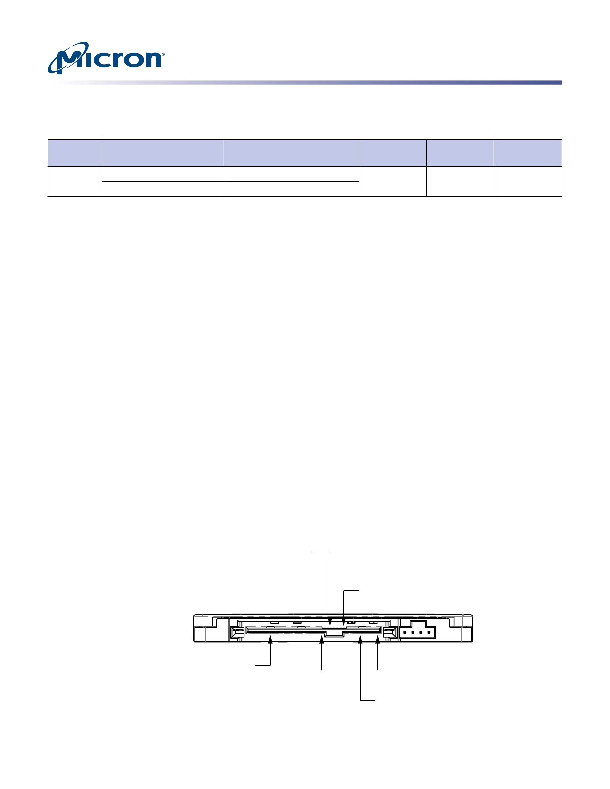
Physical Configuration
Power segment
Primary signal segment
Secondary signal segment
P1
S8
S1
Dimensions and Weight
Preliminary
S600DC Series 2.5-Inch SAS NAND Flash SSD
Physical Configuration
Form
factor Capacity (GB)
2.5-inch 200/400/480/800/960 7.00 +0.20/–0.50 69.85 ±0.25 100.24 ±0.21 TBD
1600/1920/3200/3840 15.00 +0.00/–0.50
Height
(mm)
Width
(mm)
Length
(mm)
Dual Port Support
Micron's 600 Series SAS SSD drives have two independent ports, which can be connected in the same or different SCSI domains. Each drive port has a unique SAS address.
The two ports are capable of independent port clocking. For example, both ports can
run at 12 Gb/s, or the first port can run at 12 Gb/s while the second runs at 6 Gb/s. Supported link rates are 3.0, 6.0, or 12.0 Gb/s.
Subject to buffer availability, SSD drives support the following:
• Concurrent port transfers: Supports receiving COMMAND and TASK management
transfers on both ports simultaneously
• Full duplex transfers: Supports sending XFER_RDY, DATA, and RESPONSE transfers
while receiving frames on both ports
Interface Connectors
The SAS signal segment interface cable has four transmission conductors and three
ground conductors for each channel. As shown in the figure below, the cable includes
two 7-pin signal segments (primary and secondary) and a 15-pin power segment arranged in a single row with a 1.27mm (0.050 inch) pitch.
Weight
(grams)
Figure 4: SSD Interface Connections
PDF: 09005aef8642dd23
s600dc_series_2_5_sas_ssd.pdf - Rev. F 3/16 EN
SAS drives use the device connector for the following:
• DC power
• SAS interface (dual port)
• Activity LED (DAS)
Micron Technology, Inc. reserves the right to change products or specifications without notice.
11
© 2015 Micron Technology, Inc. All rights reserved.
Page 12
S600DC Series 2.5-Inch SAS NAND Flash SSD
Pin Assignments
Table 10: Primary SAS Signal Segment Pin Assignments
Signal Name Type Description
S1 GND Second mate to ground
S2 RX0+ Positive (RX0 from target); short pin to support hot plugging
S3 RX0– Negative (RX0 from target); short pin to support hot plugging
S4 GND Second mate to ground
S5 TX0– Negative (TX0 to target); short pin to support hot plugging
S6 TX0+ Positive (TX0 to target); short pin to support hot plugging
S7 GND Second mate to ground
Table 11: Secondary SAS Signal Segment Pin Assignments – Back Side
Signal Name Type Description
S8 GND Second mate to ground
S9 RX1+ Positive (RX1 from target); short pin to support hot plugging
S10 RX1– Negative (RX1 from target); short pin to support hot plugging
S11 GND Second mate to ground
S12 TX1– Negative (TX1 to target); short pin to support hot plugging
S13 TX1+ Positive (TX1 to target); short pin to support hot plugging
S14 GND Second mate to ground
Preliminary
Physical Configuration
PDF: 09005aef8642dd23
s600dc_series_2_5_sas_ssd.pdf - Rev. F 3/16 EN
12
Micron Technology, Inc. reserves the right to change products or specifications without notice.
© 2015 Micron Technology, Inc. All rights reserved.
Page 13

S600DC Series 2.5-Inch SAS NAND Flash SSD
Physical Configuration
Table 12: SAS Power Segment Pin Assignments
Signal Name Type Description
P1 V3.3 Reserved; Short pin to support hot plugging; Behind a SAS drive plug connector, P1 and P2
are connected only to each other.
P2 V3.3 Reserved; Short pin to support hot plugging; Behind a SAS drive plug connector, P1 and P2
are connected only to each other.
P3 V3.3 No connect (vendor specific): No internal connection to drive.
P4 GND Ground
P5 GND Ground
P6 GND Ground
P7 V5 5V power (charge)
P8 V5 5V power; Short pin to support hot plugging.
P9 V5 5V power; Short pin to support hot plugging.
P10 GND Ground
P11 DAS Ready/Drive activity LED; Short pin to support hot plugging.
P12 GND Ground
P13 V12 12V power (charge)
P14 V12 12V power; Short pin to support hot plugging.
P15 V12 12V power; Short pin to support hot plugging.
Preliminary
PDF: 09005aef8642dd23
s600dc_series_2_5_sas_ssd.pdf - Rev. F 3/16 EN
13
Micron Technology, Inc. reserves the right to change products or specifications without notice.
© 2015 Micron Technology, Inc. All rights reserved.
Page 14

S600DC Series 2.5-Inch SAS NAND Flash SSD
SAS Features
Task Management
Table 13: Task Management Functions
Task Name Supported
Abort task Y
Abort task set Y
Clear ACA Y
Clear task set Y
I_T nexus reset Y
Logical unit nexus reset Y
Query task Y
Query task set Y
Query asynchronous event Y
Preliminary
SAS Features
Task Management Responses
Table 14: SAS Response to Task Management Functions
Function Name Response Code
Function complete 0
Invalid frame 2
Function not supported 4
Function failed 5
Function succeeded 8
Invalid logical unit 9
Thin Provisioning
The device supports thin provisioning and the READ CAPACITY 16 (9Eh) command, but
the level of thin provisioning support varies by product model. Thin provisioning returns a default data pattern from a READ command to a logical block even when that
block is not mapped to a physical block by a previous WRITE command.
To determine whether thin provisioning is supported and which of its features are implemented, a READ CAPACITY 16 (9Eh) command must be issued to the drive. The
LBPME (logical block provisioning management enabled) bit settings indicate whether
the logical unit implements LBPM (logical block provisioning management). The
LBPME and LBPRZ (logical block provisioning read zeros) bit settings are shown in the
table immediately below.
PDF: 09005aef8642dd23
s600dc_series_2_5_sas_ssd.pdf - Rev. F 3/16 EN
14
Micron Technology, Inc. reserves the right to change products or specifications without notice.
© 2015 Micron Technology, Inc. All rights reserved.
Page 15

Preliminary
S600DC Series 2.5-Inch SAS NAND Flash SSD
SAS Features
Table 15: Product Configuration and Bit Settings
Product Configuration
SED
Bit
LBPME Y Y LBPME = 1 (Logical unit is thin
LBPRZ N Y LBPRZ = 1 For an unmapped LBA specified by a READ opera-
Support
Non-SED
Support
Bit Settings Description
LBPM is implemented.
provisioned)
LBPME = 0 (Logical unit is fully
provisioned)
LBPRZ = 0 For an unmapped LBA specified by a READ opera-
LBPM is not implemented.
tion, the device server sends to the data-in buffer
user data with all bits set to 0.
tion, the device server sends to the data-in buffer
user data with all bits set to any value.
UNMAP Command
The UNMAP command requests that the device server break the association of a specific LBA from a physical block, thereby freeing up the physical block from use and no longer requiring it to contain user data. An unmapped block will respond to a READ command with data that is determined by the setting of the LBPRZ bit in the read capacity
parameter data.
Protection Information (PI) and Security (SED)
Requirements in this section apply to any device that supports LBA unmapping. In a
SCSI device, an umapped LBA is defined as part of the thin provisioning model, whose
support is indicated by an LBPME bit value of 1 in the read capacity parameter data.
When a cryptographic ERASE command erases a region of LBAs, the drive unmaps
those LBAs. And when the host attempts to access an unmapped or trimmed LBA, the
drive returns scrambled data.
For a given LBA, data is identical from access to access until it is either updated from
the host or is cryptographically erased. Then the drive reports an LBPRZ bit value of 0 in
the read capacity parameter data
When the host attempts access to an unmapped LBA on a drive that has been formatted
with protection information (PI), the drive returns scrambled PI data for that LBA.
Depending on the value of the RDPROTECT field in the data-access command CDB, the
drive might return a standard PI error to the host. When a host reduces a drive's addressable capacity via a MODE SELECT command, the drive unmaps or trims any LBA
within the inaccessible region of the device. Additionally, an UNMAP command is not
permitted on a locked band. PI and SED drive configuration information is shown below.
PDF: 09005aef8642dd23
s600dc_series_2_5_sas_ssd.pdf - Rev. F 3/16 EN
15
Micron Technology, Inc. reserves the right to change products or specifications without notice.
© 2015 Micron Technology, Inc. All rights reserved.
Page 16

Preliminary
S600DC Series 2.5-Inch SAS NAND Flash SSD
SAS Features
Table 16: PI and SED
Drive Configuration
PI and SED Bit Definition
PI setting Disabled Enabled Disabled Enabled
PROT_EN bit 0 1 0 1
LBPME bit 1 1 1 1
LBPRZ bit 1 1 0 0
PI check requested NA Yes No NA Yes No
DATA returned for thin
provisioned LBA
PI returned for thin
provisioned LBA
PI check performed NA No No NA Yes No
Error reported to host No No No None Yes No
Standard (Non-SED) SED
0x00 0x00 0x00 Random None Random
None 0xFF 0xFF None None Scrambled PI
data
PDF: 09005aef8642dd23
s600dc_series_2_5_sas_ssd.pdf - Rev. F 3/16 EN
16
Micron Technology, Inc. reserves the right to change products or specifications without notice.
© 2015 Micron Technology, Inc. All rights reserved.
Page 17

S600DC Series 2.5-Inch SAS NAND Flash SSD
Format Unit
The device may be formatted either as a thin provisioned device or a fully provisioned
device. Thin provisioned is the default format and is recommended for most applications. Thin provisioning provides the most flexibility for the device to manage the Flash
medium to maximize endurance.
Table 17: Format Unit Command Execution Times for 512-Byte LBAs
Preliminary
Format Unit
Format
Mode
Non-SED Configuration
Thin
provisioned
(Default)
Thin
provisioned
(Default)
Fully
provisioned
Fully
provisioned
SED Configuration
Thin
provisioned
(Default)
Thin
provisioned
(Default)
Fully
provisioned
Fully
provisioned
DCRT
BitIPBit
0 0 5 5 5 5 5 5 5 5 5 minutes
1 0 5 5 5 5 5 5 5 5 5
0 1 10 10 10 10 10 10 10 10 10
1 1 10 10 10 10 10 10 10 10 10
0 0 5 5 5 5 5 5 5 5 5 minutes
1 0 5 5 5 5 5 5 5 5 5
0 1 430 430 430 430 430 430 430 430 430
1 1 280 280 280 280 280 280 280 280 280
All S600DC Series Devices (Capacity in GB)
Unit200 400 480 800 960 1600 1920 3200 3840
PDF: 09005aef8642dd23
s600dc_series_2_5_sas_ssd.pdf - Rev. F 3/16 EN
17
Micron Technology, Inc. reserves the right to change products or specifications without notice.
© 2015 Micron Technology, Inc. All rights reserved.
Page 18

S600DC Series 2.5-Inch SAS NAND Flash SSD
Commands
Table 18: SAS Command Set and Additional Supported Bits – SED and Non-SED
Preliminary
Commands
Command
Op-Code
(Hex)
Sub-Command/
Functional Bit Description Supported
CHANGE DEFINITION 40 – – No
FORMAT UNIT 04 – – Yes
DPRY bit – No
DCRT bit – Yes
STFP bit – Yes
IP bit – Yes
DSP bit – Yes
IMMED bit – Yes
VS Vendor specific No
INQUIRY (12) 12 – – Yes
B0h Block limits page Yes
B1h Block device characteristics Yes
C1h Date code page Yes
C3h Device behavior page Yes
83h Device identification page Yes
86h Extended inquiry data page Yes
C0h Firmware numbers page Yes
C2h Jumper setting page No
8Ah Power condition page Yes
8Dh Power consumption page Yes
00h Supported vital product data
Yes
page
B2h Thin provisioning page Yes
80h Unit serial number page Yes
D1h Vendor unique page Yes
D2h Vendor unique page Yes
LOG SELECT (10) 4C – – Yes
PCR bit – Yes
DU bit – No
DS bit – Yes
TSD bit – Yes
ETC bit – No
TMC bit – No
LP bit – No
PDF: 09005aef8642dd23
s600dc_series_2_5_sas_ssd.pdf - Rev. F 3/16 EN
18
Micron Technology, Inc. reserves the right to change products or specifications without notice.
© 2015 Micron Technology, Inc. All rights reserved.
Page 19

S600DC Series 2.5-Inch SAS NAND Flash SSD
Commands
Table 18: SAS Command Set and Additional Supported Bits – SED and Non-SED (Continued)
Preliminary
Command
Op-Code
(Hex)
Sub-Command/
Functional Bit Description Supported
LOG SENSE (10) 4D – – Yes
0Fh Application client log page Yes
15h Background scan results log
Yes
page
01h Buffer over-run/under-run page No
37h Cache statistics page Yes
3Eh Factory log page Yes
2Fh Information exceptions log page Yes
0Bh Last n deferred errors or async
No
events page
07h Last n error events page No
06h Non-medium error page Yes
00h Page support list Yes
1Ah Power conditions transitions
Yes
page
18h Protocol-specific port log page Yes
03h Read error counter page Yes
04h Read reverse error counter page No
10h Self-test results page Yes
11h Solid state media log page Yes
0Eh Start-stop cycle counter page Yes
0Dh Temperature page Yes
38h Vendor unique page Yes
3Ch Vendor unique page Yes
05h Verify error counter page Yes
02h Write error counter page Yes
PDF: 09005aef8642dd23
s600dc_series_2_5_sas_ssd.pdf - Rev. F 3/16 EN
19
Micron Technology, Inc. reserves the right to change products or specifications without notice.
© 2015 Micron Technology, Inc. All rights reserved.
Page 20

S600DC Series 2.5-Inch SAS NAND Flash SSD
Commands
Table 18: SAS Command Set and Additional Supported Bits – SED and Non-SED (Continued)
Preliminary
Command
MODE SELECT (6)
MODE SELECT (10)
MODE SENSE (6)
MODE SENSE (10)
Op-Code
(Hex)
15
55
1A
5A
Sub-Command/
Functional Bit Description Supported
– – Yes
08h Caching parameters page Yes
0Ah Control mode page Yes
02h Disconnect/reconnect page Yes
01h Error recovery page Yes
03h Format page No
1Ch Information exceptions control
Yes
page
1Ch/01h Background scan mode subpage Yes
18h Protocol-specific LUN mode page Yes
19h Protocol-specific port page Yes
19h/01h Physical control and discover
Yes
subpage
19h/03h Enhanced physical control sub-
Yes
page
1Ah Power condition page Yes
00h Unit attention page Yes
07h Verify error recovery page Yes
10h XOR control page No
PERSISTENT RESERVE IN 5E – – Yes
– – Yes
00h Read keys Yes
01h Read reservations Yes
02h Read capabilities Yes
PERSISTENT RESERVE OUT 5F – – Yes
03h Clear Yes
04h Preempt Yes
05h Preempt and abort Yes
00h Register Yes
06h Register and ignore existing keys Yes
07h Register and move Yes
02h Release Yes
08h Replace lost reservation Yes
01h Reserve Yes
READ (6) 08 – – Yes
READ (10) 28 – – Yes
DPO bit supported – Yes
FUA bit supported – Yes
PDF: 09005aef8642dd23
s600dc_series_2_5_sas_ssd.pdf - Rev. F 3/16 EN
20
Micron Technology, Inc. reserves the right to change products or specifications without notice.
© 2015 Micron Technology, Inc. All rights reserved.
Page 21

S600DC Series 2.5-Inch SAS NAND Flash SSD
Commands
Table 18: SAS Command Set and Additional Supported Bits – SED and Non-SED (Continued)
Preliminary
Command
Op-Code
(Hex)
Sub-Command/
Functional Bit Description Supported
Read (12) A8 – – No
READ (16) 88 – – Yes
READ (32) 7F/0009 – – Yes
READ BUFFER
3C 1Ch Error history Yes
(Mode 0, 2, 3, A, and B)
READ CAPACITY (10) 25 – – Yes
READ CAPACITY (16) 9E/10 – – Yes
READ DEFECT DATA (10) 37 – – Yes
READ DEFECT DATA (12) B7 – – Yes
REASSIGN BLOCKS 07 – – Yes
RECEIVE DIAGNOSTIC RESULTS 1C – – Yes
00h Supported diagnostic pages Yes
40h Translate page No
RELEASE (6) 17 – – Yes
RELEASE (10) 57 – – Yes
REPORT IDENTIFYING
A3 05h – Yes
INFORMATION
REPORT LUNS A0 – – Yes
REPORT SUPPORTED OPERA-
A3 0Ch – Yes
TIONS CODES
REPORT SUPPORTED TASK
0Dh – Yes
MANAGEMENT FUNCTIONS
REQUEST SENSE 03 – – Yes
– Actual retry count bytes Yes
– Extended sense Yes
– Field pointer bytes Yes
RESERVE (6) 16 – – Yes
– 3rd party reserve Yes
– Extent reservation No
RESERVE (10) 56 – – Yes
– 3rd party reserve Yes
– Extent reservation No
REZERO UNIT 01 – – Yes
SANITIZE 48 – – Yes
01h Overwrite Yes
02h Block erase Yes
1Fh Exit failure mode Yes
SEEK (6) 0B – – Yes
PDF: 09005aef8642dd23
s600dc_series_2_5_sas_ssd.pdf - Rev. F 3/16 EN
21
Micron Technology, Inc. reserves the right to change products or specifications without notice.
© 2015 Micron Technology, Inc. All rights reserved.
Page 22

S600DC Series 2.5-Inch SAS NAND Flash SSD
Commands
Table 18: SAS Command Set and Additional Supported Bits – SED and Non-SED (Continued)
Preliminary
Command
Op-Code
(Hex)
Sub-Command/
Functional Bit Description Supported
SEEK (10) 2B – – Yes
SEND DIAGNOSTIC 1D – – Yes
00h Supported diagnostic pages Yes
40h Translate page No
SET IDENTIFYING INFORMATION A4 06h – Yes
SET TIMESTAMP 0Fh – Yes
START / STOP UNIT 1B – – Yes
SYNCHRONIZE CACHE (10) 35 – – Yes
SYNCHRONIZE CACHE (16) 91 – – Yes
TEST UNIT READY 00 – – Yes
UNMAP 42 – – Yes
VERIFY (10) 2F – – Yes
BTYCHK bit – Yes
VERIFY (12) AF – – No
VERIFY (16) 8F – – Yes
VERIFY (32) 7F/000A – – Yes
WRITE (6) 0A – – Yes
WRITE (10) 2A – – Yes
DPO bit supported – Yes
FUA bit supported Yes
WRITE (12) AA – – No
WRITE (16) 8A – – Yes
WRITE (32) 7F/0008 – – Yes
WRITE AND VERIFY (10) 2E – – Yes
DPO bit supported – Yes
WRITE AND VERIFY (12) AE – – No
WRITE AND VERIFY (16) 8E – – Yes
WRITE AND VERIFY (32) 7F/000C – – Yes
WRITE BUFFER
3B 1Ch Download application log Yes
(Modes 0 and 2 Supported)
WRITE LONG (10) 3F – – Yes
WRITE LONG (16) 9F/11 – – Yes
WRITE SAME (10) 41 – – Yes
Pbdata – No
Lbdata – No
WRITE SAME (16) 93 – – Yes
WRITE SAME (32) 7F/000D – – Yes
XDREAD 52 – – No
PDF: 09005aef8642dd23
s600dc_series_2_5_sas_ssd.pdf - Rev. F 3/16 EN
22
Micron Technology, Inc. reserves the right to change products or specifications without notice.
© 2015 Micron Technology, Inc. All rights reserved.
Page 23

S600DC Series 2.5-Inch SAS NAND Flash SSD
Commands
Table 18: SAS Command Set and Additional Supported Bits – SED and Non-SED (Continued)
Preliminary
Command
Op-Code
(Hex)
Sub-Command/
Functional Bit Description Supported
XDWRITE 50 – – No
XPWRITE 51 – – No
Table 19: SAS Command Set and Additional Supported Bits – SED Only
Op-Code
Command
(Hex)
SANITIZE 48 – Cryptographic erase Yes
SECURITY PROTOCOL IN A2 – – Yes
SECURITY PROTOCOL OUT B5 – – Yes
WRITE BUFFER
3B Modes 4, 5, and 7 Firmware download option Yes
(Modes 0 and 2 Supported)
Sub-Command/
Functional Bit Description Supported
03h
Table 20: SAS Command Set and Additional Supported Bits – Non-SED Only
Op-Code
Command
READ BUFFER
(Hex)
3C – – Yes
(Mode 0, 2, 3, A, and B)
READ LONG (10) 3E – – Yes
READ LONG (16) 9E/11 – – Yes
WRITE BUFFER
3B – Firmware download option Yes
(Modes 0 and 2 Supported)
Sub-Command/
Functional Bit Description Supported
Modes 5, 7, Ah, and Bh
PDF: 09005aef8642dd23
s600dc_series_2_5_sas_ssd.pdf - Rev. F 3/16 EN
23
Micron Technology, Inc. reserves the right to change products or specifications without notice.
© 2015 Micron Technology, Inc. All rights reserved.
Page 24

S600DC Series 2.5-Inch SAS NAND Flash SSD
Mode, Log, and VPD Pages
Table 21: Supported Mode Pages
Mode Page Code Sub-Page Code Mode Page Name
01h – Read-Write error recovery
02h – Disconnect-reconnect
07h – Verify error recovery
08h – Caching
0Ah – Control
19h – Protocol specific port
1Ah 01h Power consumption
1Ch – Informational exceptions control
Table 22: Supported Log and VPD Pages (Log Sense – 4Dh Command)
Preliminary
Mode, Log, and VPD Pages
Log Page Code (Hex) Log Page Name
0F Application client log page
15 Background scan results log page
01 Buffer over-run/under-run page
37 Cache statistics page
3E Factory log page
2F Information exceptions log page
0B Last n differed errors or async event page
07 Last n error events page (07h)
06 Non-medium error page
00 Page support list
1A Power conditions transitions page
18 Protocol-specific port log page
03 Read error counter page
04 Read reverse error counter page
10 Selt-test results page
11 Solid state media log page
0E Start-stop cycle counter page
0D Temperature page
38 Vendor unique page
3C Vendor unique page
05 Verify error counter page
02 Write error counter page
PDF: 09005aef8642dd23
s600dc_series_2_5_sas_ssd.pdf - Rev. F 3/16 EN
24
Micron Technology, Inc. reserves the right to change products or specifications without notice.
© 2015 Micron Technology, Inc. All rights reserved.
Page 25

Table 23: Internal Drive Characteristics
Characteristic Decription
Memory type NAND Flash MLC
Emulated LBA size (bytes) 512
Native programmable Page size = 8192 user bytes
Default transfer Alignment offset = 0
Preliminary
S600DC Series 2.5-Inch SAS NAND Flash SSD
Mode, Log, and VPD Pages
520
524
528
4096
4160
4192
4224
Map unit size = 4096
PDF: 09005aef8642dd23
s600dc_series_2_5_sas_ssd.pdf - Rev. F 3/16 EN
25
Micron Technology, Inc. reserves the right to change products or specifications without notice.
© 2015 Micron Technology, Inc. All rights reserved.
Page 26

S600DC Series 2.5-Inch SAS NAND Flash SSD
Reliability
A Micron SSD incorporates advanced technology for defect and error management, using various combinations of hardware-based error correction algorithms and firmwarebased static and dynamic wear-leveling algorithms.
Over the life of the SSD, uncorrectable errors may occur. An uncorrectable error is defined as data that the device reports as successfully programmed, but when read, the
data differs from what was programmed.
The following reliability specifications assume correct host and drive operational interface, including all interface timings, power supply voltages, environmental requirements, and drive mounting constraints.
Table 24: Uncorrectable Bit Error Rate
Read Error Rates READ Operation
Less than 1 LBA in 1017 bits transferred Unrecovered READ
Less than 1 LBA in 1021 bits transferred Mis-corrected READ
Preliminary
Reliability
Note:
1. Error rate specified with automatic retries and data correction with ECC enabled and all
flaws reallocated.
Mean Time between Failures
SSD mean time to failure (MTTF) and mean time between failures (MTBF) are predictable based on component reliability data using the methods referenced in the Telcordia
SR-332 reliability prediction procedures for electronic equipment.
Table 25: MTBF
Capacity
200GB 2.5 0.35
400GB 2.5 0.35
480GB 2.5 0.35
800GB 2.5 0.35
960GB 2.5 0.35
1600GB 2.5 0.35
1920GB 2.5 0.35
3200GB 2.5 0.35
3840GB 2.5 0.35
MTBF (Million Hours) Failure Rate (% per-Year)
All S600DC Series Devices
PDF: 09005aef8642dd23
s600dc_series_2_5_sas_ssd.pdf - Rev. F 3/16 EN
26
Micron Technology, Inc. reserves the right to change products or specifications without notice.
© 2015 Micron Technology, Inc. All rights reserved.
Page 27

S600DC Series 2.5-Inch SAS NAND Flash SSD
Data Retention
As a NAND Flash device ages with use, its capability to retain a programmed value is
affected by the number of PROGRAM and ERASE operations to its cells, causing deterioration. When new, the device has a powered-off data retention capability of several
years, but with use, data retention is reduced.
Temperature also affects how long the device retains its programmed value when power
is removed. High temperature reduces retention capability when power is off, but is not
an issue when power is applied. The SSD drive contains firmware and hardware features that can monitor and refresh memory cells when power is applied.
Table 26: Data Retention and Drive Writes per-Day
Preliminary
Reliability
Device and Capacity
S655DC
200GB 3 25
400GB 3 25
S650DC
400GB 3 10
800GB 3 10
1600GB 3 10
3200GB 3 10
S630DC
400GB 3 3
480GB 3 3
800GB 3 2
960GB 3 3
1600GB 3 2
1920GB 3 3
3200GB 3 2
3840GB 3 3
S610DC
1920GB 3 <1
3840GB 3 <1
Typical Data Retention
with Power Removed (Months)
1
Drive Writes per-Day (DWPD)
Note:
PDF: 09005aef8642dd23
s600dc_series_2_5_sas_ssd.pdf - Rev. F 3/16 EN
1. Typical data retention with power removed, at 40 °C and up to 90% of write endurance.
27
Micron Technology, Inc. reserves the right to change products or specifications without notice.
© 2015 Micron Technology, Inc. All rights reserved.
Page 28

Endurance
Table 27: Endurance
Device and Capacity Endurance Unit
S655DC
S650DC
S630DC
S610DC
Preliminary
S600DC Series 2.5-Inch SAS NAND Flash SSD
Reliability
Endurance rating is the expected amount of host data that can be written by product
when subjected to a specified workload at a specified operating and storage temperature over the specified product life. For the specific workload to achieve this level of endurance, refer to JEDEC specification JESD218. TBW is defined as 1 x 1012 bytes.
200GB 8000 TBW
400GB 17,000
400GB 7000 TBW
800GB 14,000
1600GB 29,000
3200GB 58,000
400GB 2100 TBW
480GB 2600
800GB 2900
960GB 5200
1600GB 5800
1920GB 10,000
3200GB 12,000
3840GB 21,000
1920GB 2800 TBW
3840GB 5600
Notes:
PDF: 09005aef8642dd23
s600dc_series_2_5_sas_ssd.pdf - Rev. F 3/16 EN
1. Limited warranty with media usage provides coverage either for the warranty period or
until the SSD percentage used endurance indicator reaches 100, whichever comes first.
2. TBW per the JEDEC JESDS218 specification assuming typical workloads are 50% sequential and 50% random and consist of the following: 5% are 4KB; 5% are 8KB; 10% are
16KB; 10% are 32KB; 35% are 64KB; and 35% are 128KB.
28
Micron Technology, Inc. reserves the right to change products or specifications without notice.
© 2015 Micron Technology, Inc. All rights reserved.
Page 29

Electrical Characteristics
Device DC power (+12V and +5V) is through the standard SAS interface. Typical power
measurements listed below are based on an average of drives tested, under nominal
conditions, using the listed input voltage at 60°C internal temperature. Measurements
are made at 12Gb interface speeds.
• Startup power: Measured from power-on to when the drive reaches operating condition and can process media access commands.
• Peak operating mode power: Measured by testing the drive in various read and write
access patterns that simulate worst case power consumption.
• Idle mode power: Measured when the drive is powered up and ready for media access
commands, but before the host has sent the commands.
Note: Stresses greater than those listed in the following tables may cause permanent
damage to the device. These are stress ratings only and device operation above ratings
or conditions listed in the operation sections of this specification is not implied. Exposure to absolute maximum rating conditions for extended periods may affect reliability.
Preliminary
S600DC Series 2.5-Inch SAS NAND Flash SSD
Electrical Characteristics
PDF: 09005aef8642dd23
s600dc_series_2_5_sas_ssd.pdf - Rev. F 3/16 EN
29
Micron Technology, Inc. reserves the right to change products or specifications without notice.
© 2015 Micron Technology, Inc. All rights reserved.
Page 30

Power Consumption
Specifications
Table 28: Power Consumption Specifications
Preliminary
S600DC Series 2.5-Inch SAS NAND Flash SSD
Electrical Characteristics
Average Power
Device
and
Capacity
VDC Start Current
1
Power
(W)
Average Idle
Power (W)
Under Workload (W)
Sequential
Sequential
Read
Write
2
Configurable Power
Limit Settings+5A +12A
S655DC
200GB 1.05 0.34 9.29 3.54 5.10 6.79 6, 7, 8, 9, 10, 11
400GB 1.05 0.34 9.29 3.54 5.10 6.79 6, 7, 8, 9, 10, 11
S650DC
400GB 1.05 0.34 9.29 3.54 5.10 6.79 6, 7, 8, 9, 10, 11
800GB 1.05 0.34 9.29 3.54 5.10 6.79 6, 7, 8, 9, 10, 11
1600GB 0.93 0.50 10.62 4.14 7.33 10.78 8, 9, 10, 11, 12, 13, 14
3200GB 0.94 0.61 12.06 5.40 9.15 13.15 9, 10, 11, 12, 13, 14, 15
S630DC
400GB 1.05 0.34 9.29 3.54 5.10 6.79 6, 7, 8, 9, 10, 11
480GB 1.05 0.34 9.29 3.54 5.10 6.79 6, 7, 8, 9, 10, 11
800GB 1.05 0.34 9.29 3.54 5.10 6.79 6, 7, 8, 9, 10, 11
960GB 1.05 0.34 9.29 3.54 5.10 6.79 6, 7, 8, 9, 10, 11
1600GB 0.93 0.50 10.62 4.14 7.33 10.78 8, 9, 10, 11, 12, 13, 14
1920GB 0.90 0.49 10.41 4.17 7.36 10.65 8, 9, 10, 11, 12, 13, 14
3200GB 0.94 0.61 12.06 5.40 9.15 13.15 9, 10, 11, 12, 13, 14, 15
3840GB 0.98 0.59 11.96 5.93 9.29 13.30 9, 10, 11, 12, 13, 14, 15
S610DC
1920GB 0.90 0.49 10.41 4.17 7.36 10.65 8, 9, 10, 11, 12, 13, 14
3840GB 0.98 0.59 11.96 5.93 9.29 13.30 9, 10, 11, 12, 13, 14, 15
Notes:
1. Measured with average reading DC ammeter. Instantaneous +12V current peaks will exceed these values. Power supply at nominal voltage. Number of drives tested = 6 at 60
°C internal.
2. Sequential READ and WRITE operations are based on 128K block transfer at queue
depth = 32.
Identifier and Supported Settings
Supported power consumption identifier settings are shown in the table below. An INQUIRY SCSI command or MODE SENSE command can be used to query VPD page
0x8D for supported power levels and associated identifiers.
The MODE SENSE and SELECT commands can be used to read, write, and modify the
mode page 0x1A, subpage 1. When the SELECT command is used to write a new identifier value, the value is saved in nonvolatile memory, unchanged until modified.
PDF: 09005aef8642dd23
s600dc_series_2_5_sas_ssd.pdf - Rev. F 3/16 EN
30
Micron Technology, Inc. reserves the right to change products or specifications without notice.
© 2015 Micron Technology, Inc. All rights reserved.
Page 31

S600DC Series 2.5-Inch SAS NAND Flash SSD
Table 29: Power Consumption Identifier and Supported Settings
Note 2 applies to entire table.
Mode Page
Device and
Capacity
S655DC
200GB 11 10 9 8 7 6 N/A W
400GB 11 10 9 8 7 6 N/A
S650DC
400GB 11 10 9 8 7 6 N/A W
800GB 11 10 9 8 7 6 N/A
1600GB 14 13 12 11 10 9 8
3200GB 15 14 13 12 11 10 9
S630DC
400GB 11 10 9 8 7 6 N/A W
480GB 11 10 9 8 7 6 N/A
800GB 11 10 9 8 7 6 N/A
960GB 11 10 9 8 7 6 N/A
1600GB 14 13 12 11 10 9 8
1920GB 14 13 12 11 10 9 8
3200GB 15 14 13 12 11 10 9
3840GB 15 14 13 12 11 10 9
S610DC
1920GB 14 13 12 11 10 9 8 W
3840GB 15 14 13 12 11 10 9
0x0
(Default) 0x1 0x2 0x3 0x4 0x5 0x6
Preliminary
Electrical Characteristics
Unit
Note:
1. Device settings can be configured by modifying VPD mode page 0x1A, subpage 0x1.
Power
Table 30: Power Specifications
Parameter/Condition VDC (Margin) Min Max Unit
Voltage input – Start up 12 (±10%) 10.8 13.2 V
Voltage input – Steady state 12 (±5%) 11.4 12.6
Voltage input 5 (±5%) 4.75 5.25
PDF: 09005aef8642dd23
s600dc_series_2_5_sas_ssd.pdf - Rev. F 3/16 EN
31
Micron Technology, Inc. reserves the right to change products or specifications without notice.
© 2015 Micron Technology, Inc. All rights reserved.
DC
Page 32

Preliminary
S600DC Series 2.5-Inch SAS NAND Flash SSD
Electrical Characteristics
Environmental Specifications
Table 31: Environmental Specifications – 1
Parameter/Condition Min Max Unit
Operating temperature
Non-operating temperature –40/–40 165/75
Rate of temperature change – 36/20
Relative humidity (non-condensing) 5 95 %rh
Relative humidity (rate of change /hr) – 20
Effective altitude (operating) –1000/304.8 10,000/3048 ft/M
Effective altitude (non-operating) –1000/304.8 40,000/12,192
1
32/0 122/50 °F/°C
Note:
1. Based on ambient air temperature
Table 32: Environmental Specifications – 2
Parameter Condition Max Unit
Operating shock (half sine wave) Gs 1000 g
Duration 0.5 ms
Interval 2 sec
Non-operating shock (half sine wave) Gs 1000 g
Duration 0.5 ms
Interval 2 sec
PDF: 09005aef8642dd23
s600dc_series_2_5_sas_ssd.pdf - Rev. F 3/16 EN
32
Micron Technology, Inc. reserves the right to change products or specifications without notice.
© 2015 Micron Technology, Inc. All rights reserved.
Page 33

Regulatory Compliance
Micron SSDs comply with the following:
• RoHS
• CE (Europe): EN55022, 2006 + A1:2007 and EN55024, 1998 + A1: 2001 + A2:2003
• FCC: CFR Title 47, Part 15 Class A
• UL (US): approval to UL-60950-1, 2nd Edition, IEC 60950-1:2005, 2nd Edition; Am
1:2009, EN 60950-1 (2006) + A11:2009+ A1:2010 + A12:2011
• BSMI (Taiwan): approval to CNS 13438
• C-TICK (Australia, New Zealand): approval to AS/NZS CISPR22
• KCC RRL (Korea): approval to KCC-REM-MU2
• W.E.E.E.: Compliance with EU WEEE directive 2002/96/EC. Additional obligations
may apply to customers who place these products in the markets where WEEE is enforced.
• TUV (Germany): approval to IEC60950/EN60950
• V
CCI
Preliminary
S600DC Series 2.5-Inch SAS NAND Flash SSD
Regulatory Compliance
FCC Rules
This equipment has been tested and found to comply with the limits for a Class A digital
device, pursuant to part 15 of the FCC rules. These limits are designed to provide reasonable protection against harmful interference when the equipment is operated in a
commercial environment.. This equipment generates, uses, and can radiate radio frequency energy and, if not installed and used in accordance with the instruction manual,
may cause harmful interference to radio communications. Operation of this equipment
in a residential area is likely to cause harmful interference in which case the user will be
required to correct the interference at one’s own expense.
PDF: 09005aef8642dd23
s600dc_series_2_5_sas_ssd.pdf - Rev. F 3/16 EN
33
Micron Technology, Inc. reserves the right to change products or specifications without notice.
© 2015 Micron Technology, Inc. All rights reserved.
Page 34

Package Dimensions
S
Connector
C
L
C
L
Connector end
Connector end
3.50 ±0.38
(A7 ±A12)
7.00
+0.20
-0.50
1.50 MIN (A15)
Drive
14.00 (A50)
4.80 (A11)
9.40 (A8)
4.07 (A28)
90.60 (A51)
X
4 places
minimmum 2 (A38) thread
reference
4 places
minimmum 2.5 (A41) thread
reference
B
B-B
(rotated 90° CCW)
B
(100.54)
(100.50) (A11))
3
61.72 (A29)
69.85 ±0.25 (A4 ±A5)
14.00 (A52)
3.00 (A23)
90.60 (A53)
100.24
(100.45 MAX (A6))
3
X Y Z0.50 (A27)
4X M3 (A26)
MIN 2 (A38) full THD
X Y Z0.50 (A33)
4X M3 (A32)
MIN 2.5 (A41) full THD
(0.30) (A18)
(A1 +A2/-A3)
Y
X
X
Z
S
2.5-Inch Package – 7mm
Figure 5: 2.5-Inch Package – 7mm
Preliminary
S600DC Series 2.5-Inch SAS NAND Flash SSD
Package Dimensions
PDF: 09005aef8642dd23
s600dc_series_2_5_sas_ssd.pdf - Rev. F 3/16 EN
34
Micron Technology, Inc. reserves the right to change products or specifications without notice.
© 2015 Micron Technology, Inc. All rights reserved.
Page 35

2.5-Inch Package – 15mm
C
L
Connector
Drive
C
L
Connector end
Connector end
15.00
+0.00
-0.50
(A1 +A2/-A3)
3.50 ±0.38
(A7 ±A12)
1.50 MIN (A15)
14.00 (A50)
4.80 (A11)
9.40 (A8)
4.07 (A28)
90.60 (A51)
X
4 places
minimmum 2 (A38) thread
reference
4 places
minimmum 2.5 (A41) thread
reference
B
Section B-B
(rotated 90° CCW)
B
(100.54)
(100.50) (A11))
3
61.72 (A29)
69.85 ±0.25 (A4 ±A5)
14.00 (A52)
3.00 (A23)
90.60 (A53)
100.24
(100.45 MAX (A6))
3
X Y Z0.50 (A27)
4X M3 (A26)
MIN 2 (A38) full THD
X Y Z0.50 (A33)
4X M3 (A32)
MIN 2 (A41) full THD
(0.30) (A18)
Y
X
X
Z
S
S
Figure 6: 2.5-Inch Package – 15mm
Preliminary
S600DC Series 2.5-Inch SAS NAND Flash SSD
Package Dimensions
PDF: 09005aef8642dd23
s600dc_series_2_5_sas_ssd.pdf - Rev. F 3/16 EN
35
Micron Technology, Inc. reserves the right to change products or specifications without notice.
© 2015 Micron Technology, Inc. All rights reserved.
Page 36

SAS References
Preliminary
S600DC Series 2.5-Inch SAS NAND Flash SSD
SAS References
• Serial Attached SCSI-3 (SAS-3)
• SCSI Architecture Model-5 (SAM-5)
• SCSI Primary Commands-3 (SPC-3)
• SCSI Primary Commands-4 (SPC-4)
• SCSI ATA Translation-2 (SAT-2)
• SCSI Block Commands-3 (SBC-3)
PDF: 09005aef8642dd23
s600dc_series_2_5_sas_ssd.pdf - Rev. F 3/16 EN
36
Micron Technology, Inc. reserves the right to change products or specifications without notice.
© 2015 Micron Technology, Inc. All rights reserved.
Page 37

Revision History
Rev. F – 3/16
Rev. E – 12/15
Rev. D – 11/15
Rev. C – 9/15
Rev. B – 6/15
Preliminary
S600DC Series 2.5-Inch SAS NAND Flash SSD
Revision History
• Updated LBA setting tables, power matrix table, performance numbers, and endurance specifications.
• Updated Performance table in Features section
• Revised maximum operating temperature to 50°C
• Revised specifications, densities, and MPNs
Rev. A – 5/15
• Revised specifications, densities, and MPNs
• Initial release
8000 S. Federal Way, P.O. Box 6, Boise, ID 83707-0006, Tel: 208-368-4000
www.micron.com/products/support Sales inquiries: 800-932-4992
Micron and the Micron logo are trademarks of Micron Technology, Inc.
All other trademarks are the property of their respective owners.
This data sheet contains initial characterization limits that are subject to change upon full characterization of production devices.
PDF: 09005aef8642dd23
s600dc_series_2_5_sas_ssd.pdf - Rev. F 3/16 EN
37
Micron Technology, Inc. reserves the right to change products or specifications without notice.
© 2015 Micron Technology, Inc. All rights reserved.
 Loading...