

Page 1

P320h HHHL PCIe NAND SSD
Features
P320h Half-Height and Half-Length PCIe NAND Flash SSD
MTFDGARxxxSAH-1Nxxx
Features
• Micron® SLC NAND Flash (34nm)
• ONFI 2.1-compliant Flash Interface
• PCIe Gen2 x8 host interface
• Capacity:1 350GB, 700GB
• Endurance (total bytes written)
– 350GB: 25PB (4KB random write),
50PB (128KB sequential write)
– 700GB: 50PB (4KB random write),
100PB (128KB sequential write)
• Temperature
– Operating: 0°C to +85°C
– Storage (in system): 0°C to +40°C
– Storage (on shelf): –40°C to +85°C
– Temperature throttling support
• ATA modes supported
– PIO modes 3 and 4
– Multiword DMA modes 0, 1, 2
– Ultra DMA modes 0, 1, 2, 3, 4, 5, 6
– ATA8-ACS2 command set support
– ATA security feature command set and password
login support
• Industry-standard 512-byte sector size support
• Full end-to-end data protection
• Native command queuing up to 256 commands
• Bootable
6
• Power: 25W RMS
• Random read/write (steady state) performance at
7
25W
– Random read: Up to 785,000 IOPS (4KB)
– Random write: Up to 205,000 IOPS (4KB)
• Sequential read/write (steady state) performance at
7
25W
– Sequential read: Up to 3.2 GB/s (128KB)
– Sequential write: Up to 1.9 GB/s (128KB)
• Latency (queue depth = 1)
– READ latency: <47µs
– WRITE latency: <311µs (nonposted)
• Custom drivers
– Windows Server 2012 R2 (x86-64), Hyper-V
(x86-64)
– Windows Server 2012 (x86-64), Hyper-V (x86-64)
2, 3
4
5
5
7
– Windows Server 2008 R2 SP1 (x86-64), Hyper-V
(x86-64)
– Windows 8, 8.1 (x86-64 and x86)
– Windows 7 (x86-64 and x86)
– RHEL 5.5–5.10, 6.0–6.5, 7 (x86-64)
– SLES 11 SP1, SP2, SP3 (x86-64)
– VMware 5.0, 5.1 (x86-64)
– VMware 5.5 (inbox driver)
– Citrix XenServer 6.0.2, 6.1, 6.2
– Ubuntu 12.04–12.04.4, 14.04 LTS Server (64-bit)
• Reliability
– MTTF: 2 million hours
– Static and dynamic wear leveling
– Field-upgradable firmware
– Uncorrectable bit error rate (UBER): <1 sector
per 1017 bits read
• Micron RAIN (redundant array of independent
NAND) technology
• SMART command set support
• On-chip temperature monitoring
• Mechanical/electrical
– 68.90mm x 167.65mm x 18.71mm
– PCIe-compliant, x8 lane PCB connector
– 12V power (±8%)
– Weight: 350GB – 127.2g; 700GB – 135.3g
• Shock: 400g at 2ms
• Vibration: 3.1 grms 5–500Hz at 30 min/axis
• RoHS-compliant
Notes:
1. User capacity: 1GB = 1 billion bytes.
2. Lifetime endurance is measured not in
years, but in the number of bytes that can
be written to the device.
3. Workloads are 100% writes.
4. Operating temperature is the drive case
temperature as measured by the SMART
temperature attribute.
5. Assumes system is powered off and ready to
be powered on.
6. Bootable option determined by part number; see Part Numbering Information
(page 2). Boot ability may not be compatible on some systems.
7. Values vary by capacity. See Performance
Specifications (page 4) for details.
PDF: 09005aef848cbdf4
realssd_p320h_hhhl_distribution.pdf - Rev. V 8/2014 EN
Products and specifications discussed herein are subject to change by Micron without notice.
1
Micron Technology, Inc. reserves the right to change products or specifications without notice.
© 2011 Micron Technology, Inc. All rights reserved.
Page 2
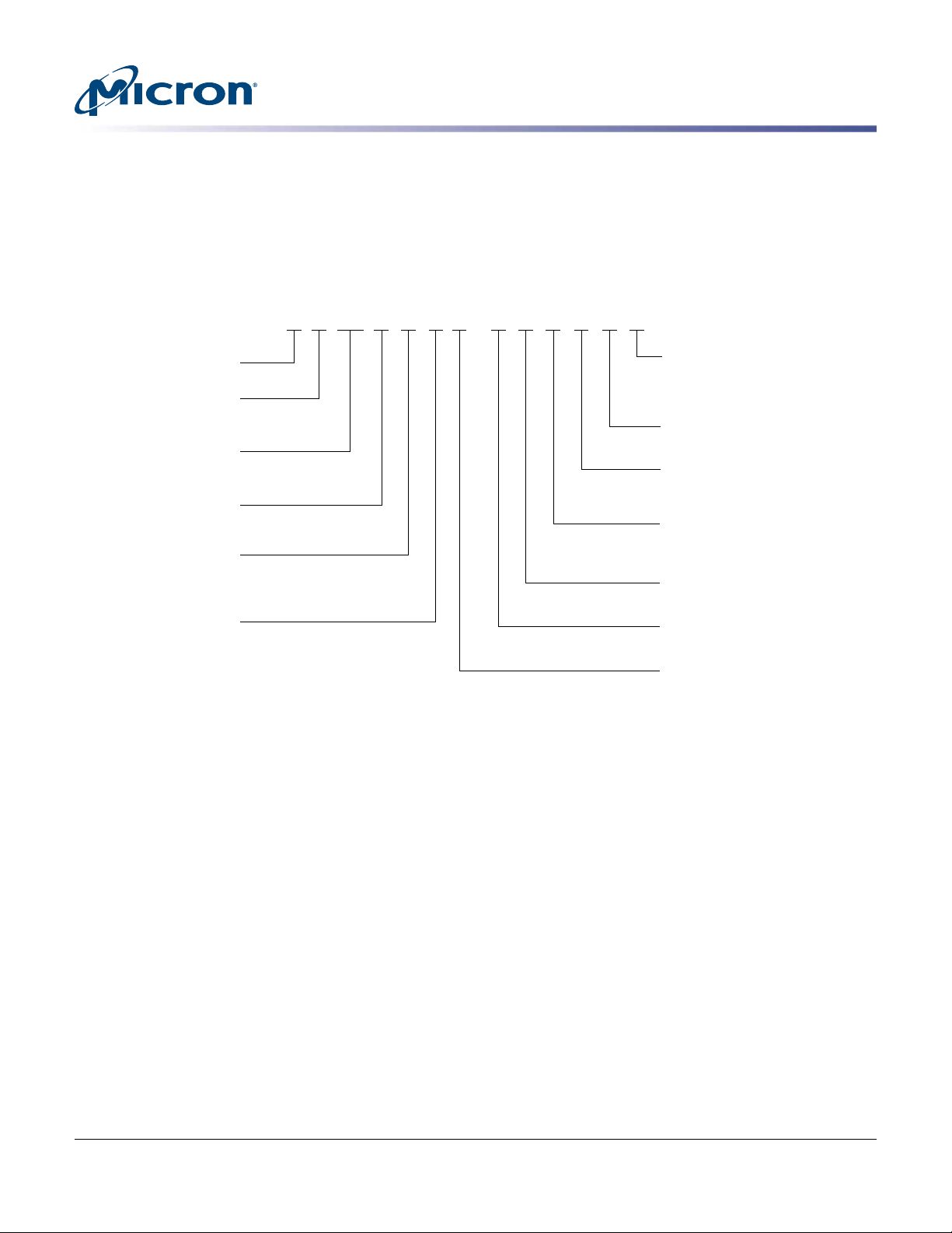
MT FD G
350
S
Micron Technology
Product Family
FD = Flash drive
Drive Interface
G = PCIe Gen2
Drive Form Factor
AR = Half height, half length, x8
Device Density
350 = 350GB
700 = 700GB
NAND Flash Type
S = SLC
Production Status
Blank = Production
ES = Engineering sample
MS = Mechanical sample
Hardware Feature Set
AB = Contact factory
BOM Revision
1 = First generation
A to Z = ES designation
NAND Component
N = 16Gb, SLC, x8, 3.3V (34nm)
Sector Size
1 = 512 byte
Flash Drive Product Family
AH = P320H
AR
AH – 1
A
AB ES
N
Security Feature Set
Blank = Default
4 = Bootable
4
P320h HHHL PCIe NAND SSD
Features
Part Numbering Information
The Micron® P320h SSD is available in different configurations and densities. Visit www.micron.com for a list of
valid part numbers.
Figure 1: Part Number Chart
Warranty: Contact your Micron sales representative for further information regarding the product,
including product warranties.
PDF: 09005aef848cbdf4
realssd_p320h_hhhl_distribution.pdf - Rev. V 8/2014 EN
2
Micron Technology, Inc. reserves the right to change products or specifications without notice.
© 2011 Micron Technology, Inc. All rights reserved.
Page 3
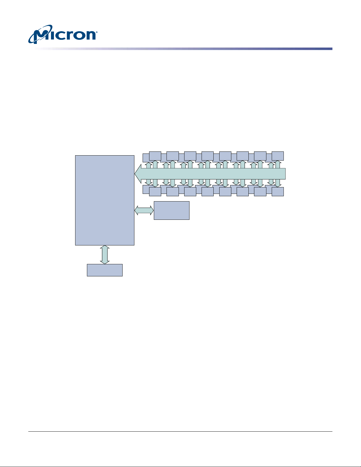
General Description
NAND
NAND
NAND
NAND
NAND
NAND
NAND
NAND
NAND
NAND
NAND
NAND
NAND
NAND
NAND
NAND
32 channels, 64 placements of NAND memory
DDR3
DRAM
PCIe x 8 edge
connector
NAND Storage
Controller
Micron's P320h solid state drive (SSD) is targeted at applications that require high performance and enterprise-class storage reliability. The P320h delivers extremely high
IOPS performance due to its ability to support up to 256 outstanding commands while
ensuring full end-to-end data protection.
The P320h comes in a half-height, half-length (HHHL) form factor and uses a secondgeneration (Gen2) PCIe x8 lane interface on the host side and 32 ONFI 2.1-compliant
channels on the Flash side.
Figure 2: Functional Block Diagram
P320h HHHL PCIe NAND SSD
General Description
PDF: 09005aef848cbdf4
realssd_p320h_hhhl_distribution.pdf - Rev. V 8/2014 EN
3
Micron Technology, Inc. reserves the right to change products or specifications without notice.
© 2011 Micron Technology, Inc. All rights reserved.
Page 4
P320h HHHL PCIe NAND SSD
Architecture
Architecture
The single-chip, Micron-developed ASIC controller, along with the host and Flash interfaces, provide an embedded ATA host bus adapter, a host/Flash translation layer, Flash
maintenance, channel control, and Flash RAID (RAIN) protection.
Flash endurance and reliability are optimized through the Flash maintenance features,
including static and dynamic wear leveling and RAIN protection. Most of these functions are implemented directly within the controller hardware to optimize performance. The device is shipped in the configurations shown below.
Table 1: P320h HHHL Configurations
User Capacity NAND Flash Process NAND Flash Density Package Count Die per BGA Package
350GB 34nm 16Gb 64 4
700GB 34nm 16Gb 64 8
Performance Specifications
Table 2: Performance Specifications
Specification 350GB 700GB
Sequential read (up to) 3.2 GB/s 3.2 GB/s
Sequential write (up to) 1.9 GB/s 1.9 GB/s
Random read (up to) 785,000 IOPS 785,000 IOPS
Random write (up to) 175,000 IOPS 205,000 IOPS
READ latency <47µs <47µs
WRITE latency <311µs (nonposted) <311µs (nonposted)
Notes:
1. Transient peaks above 25W are possible under heavy write workloads. 10ms RMS average measurements taken.
2. Drive is erased and filled with zeroes to achieve preconditioned state .
3. 128KB transfers are used for sequential read/write values; 4KB transfers are used for
random read/write values.
4. I/O performance numbers are measured in steady state using FIO with a preconditioned
drive under RHEL 6.3 with a queue depth of 256 and with raw device access on systems
with a single Intel Xeon E5-2667 2.90 GHz processor with 6 cores, 12 logical and hyperthreading enabled.
5. Steady state performance is defined as conforming to the SNIA V1.0 Performance Test
Specification.
6. Performance numbers derived from tests at room temperature.
7. Latency performance numbers are measured using FIO with queue depth 1, random
transfer, 512-byte transfer size for READ latency, 4KB transfer size for WRITE latency.
8. Performance numbers are notated in base 10.
PDF: 09005aef848cbdf4
realssd_p320h_hhhl_distribution.pdf - Rev. V 8/2014 EN
4
Micron Technology, Inc. reserves the right to change products or specifications without notice.
© 2011 Micron Technology, Inc. All rights reserved.
Page 5

Functional Description
Data Retention
Data retention refers to the SSD's media (NAND Flash) capability to retain programmed
data when the SSD is powered off. The two primary factors that influence data retention
are degree of use (the number of PROGRAM/ERASE cycles on the media) and temperature.
Degree of use: As NAND Flash is used (programmed and erased), its natural ability to
retain charge (programmed data) decreases. When the SSD ships from the factory, it is
typically able to retain user data for up to 10 years when powered off. As the SSD is used,
this typically decreases to one year.
Temperature: As the temperature increases, data retention decreases.
Note: All data retention related to values in the data sheet are with the SSD powered off.
When the SSD is powered on, data retention is expected to exceed these limits. Micron
SSD data retention with power removed is one year at 40°C (MAX).
Micron RAIN Technology
Redundant array of independent NAND (RAIN) is a technology developed by Micron
designed to extend the lifespan of the P320h.
P320h HHHL PCIe NAND SSD
Functional Description
Wear Leveling
Residing in the P320h ASIC controller, RAIN is similar to redundant array of independent disks (RAID) technology, but instead of grouping and striping disks, RAIN groups
and stripes storage elements on the SSD across multiple channels, generating and storing parity data along with user data (one page of parity for every seven pages of user
data). This data structure (user data plus parity) enables complete, transparent data recovery if a single storage element (NAND page, block, or die) fails. If a failure occurs, the
P320h automatically detects it and transparently rebuilds the data. During this RAIN rebuild process, the drive's performance is reduced temporarily but will recover after the
rebuild process completes.
Wear leveling is a technique that spreads Flash block use over the entire memory array
to equalize the PROGRAM/ERASE cycles on all blocks in the array. This helps to enhance the lifespan of the SSD. The P320h supports both static and dynamic wear leveling.
Static wear leveling considers all Flash blocks in the SSD regardless of data content or
access and maintains an even level of wear across the drive. Dynamic wear leveling
monitors available free space on the drive and dynamically moves data between Flash
blocks to equalize wear on each block. Both techniques are used together within the
controller to optimally balance the wear profile of the Flash array along with the drive's
lifespan.
PDF: 09005aef848cbdf4
realssd_p320h_hhhl_distribution.pdf - Rev. V 8/2014 EN
5
Micron Technology, Inc. reserves the right to change products or specifications without notice.
© 2011 Micron Technology, Inc. All rights reserved.
Page 6
SMART Attribute Summary
P320h HHHL PCIe NAND SSD
SMART Attribute Summary
Table 3: SMART Command Reference
1
Attribute ID Hex ID Name SMART Trip Description
9 0x09 Power-on hours count No Lifetime powered-on hours, from the time the
device leaves the factory
12 0x0C Power cycle count No Count of power cycles
170 0xAA New failing block
No Grown defects
count
171 0xAB Program fail count No Number of NAND program status failures
172 0xAC Erase fail count No Number of NAND erase status failures
174 0xAE Unexpected power loss
No Number of unexpected power-loss occurrences
count
187 0xBB Reported uncorrecta-
No Number of ECC correction failures
ble errors count
188 0xBC Command timeout
count
No Number of command timeouts, defined by an
active command being interrupted by a HRESET,
COMRESET, SRST, or other command
194 0xC2 Temperature No The on-die temperature sensor within the con-
troller ASIC in degrees C, capturing the lifetime
high and low temperatures measured
202 0xCA Percentage of the rat-
ed lifetime used
No Cumulative erase count / lifetime erase count as
expressed as a percent. Lifetime erase count is
the total number of available blocks * block endurance for the flash technology, read directly
from the NAND device.
232 0xE8 Available reserved
space
No Percentage of spare blocks remaining
Spare block count
241 0xF1 Power-on (minutes) No Lifetime power-on time in minutes
242 0xF2 Write protect progress No Progress toward WRITE PROTECT mode: reports
100% when the drive becomes read only
Note:
PDF: 09005aef848cbdf4
realssd_p320h_hhhl_distribution.pdf - Rev. V 8/2014 EN
1. Attribute/Hex IDs are noted for distribution product. Specific OEMs may have different
ID values, but the same list of SMART commands applies.
6
Micron Technology, Inc. reserves the right to change products or specifications without notice.
© 2011 Micron Technology, Inc. All rights reserved.
Page 7

P320h HHHL PCIe NAND SSD
Logical Block Address Configuration
Logical Block Address Configuration
The number of logical block addresses (LBAs) reported by the P320h ensures sufficient
storage space for the specified capacity. Standard LBA settings based on the IDEMA
standard (LBA1-02) are shown below.
Table 4: Standard LBA Settings
Total LBA Max LBA User Available
Bytes (Unformat-
Capacity
350GB 683,747,568 28C128F0 683,747,567 28C128EF 350,078,754,816
700GB 1,367,473,968 5181FF30 1,367,473,967 5181FF2F 700,146,671,616
ted)Decimal Hexadecimal Decimal Hexadecimal
Note:
1. Note: 1GB = 1 billion bytes; user capacity.
Physical Configuration
Table 5: Nominal Dimensions and Weight
Specification Value Unit
Height 68.90 mm
Width 18.71 mm
Length 167.65 mm
Unit weight (HH bracket) 350GB: 127.2
700GB: 135.3
Unit weight (FH bracket) 350GB: 132.3
700GB: 140.4
g
g
PDF: 09005aef848cbdf4
realssd_p320h_hhhl_distribution.pdf - Rev. V 8/2014 EN
7
Micron Technology, Inc. reserves the right to change products or specifications without notice.
© 2011 Micron Technology, Inc. All rights reserved.
Page 8

Interface Connectors
The host interface connector conforms to the PCIe Electromechanical Specification
V2.0, section 5, Table 5-1. It is an eight-lane, gold-finger connector with 1mm pitch
spacing.
A mechanical indent is used to separate the PCIe power pins from the differential signal
contacts. The pins are numbered below in ascending order from left to right. Side B refers to component side and Side A refers to the solder side.
Table 6: PCIe Interface Connector Pin Assignments
P320h HHHL PCIe NAND SSD
Interface Connectors
Pin
Number
1 +12V 12V power PRSNT1# Hot Plug Presence Detect
2 +12V 12V power +12V 12V power
3 +12V 12V power +12V 12V power
4 GND Ground GND Ground
5 SMCLK DNU JTAG2 DNU
6 SMDAT DNU JTAG3 DNU
7 GND Ground JTAG4 DNU
8 +3.3V DNU JTAG5 DNU
9 JTAG1 DNU +3.3V DNU
10 3.3Vaux DNU +3.3V DNU
11 WAKE# DNU PERST# PCIe Reset
Mechanical Key
12 RSVD Reserved GND Ground
13 GND Ground REFCLK+ PCIe REFCLK p
14 PETp0 PCIe TX Lane 0 p REFCLK- PCIe REFCLK n
15 PETn0 PCIe TX Lane 0 n GND Ground
16 GND Ground PERp0 PCIe RX Lane 0 p
17 PRSNT2# Hot Plug Presence Detect PERn0 PCIe RX Lane 0 n
18 GND Ground GND Ground
19 PETp1 PCIe TX Lane 1 p RSVD Reserved
20 PETn1 PCIe TX Lane 1 n GND Ground
21 GND Ground PERp1 PCIe RX Lane 1 p
22 GND Ground PERn1 PCIe RX Lane 1 n
23 PETp2 PCIe TX Lane 2 p GND Ground
24 PETn2 PCIe TX Lane 2 n GND Ground
25 GND Ground PERp2 PCIe RX Lane 2 p
26 GND Ground PERn2 PCIe RX Lane 2 n
27 PETp3 PCIe TX Lane 3 p GND Ground
28 PETn3 PCIe TX Lane 3 p GND Ground
29 GND Ground PERp3 PCIe RX Lane 3 p
Name Description Name Description
Side B Side A
PDF: 09005aef848cbdf4
realssd_p320h_hhhl_distribution.pdf - Rev. V 8/2014 EN
8
Micron Technology, Inc. reserves the right to change products or specifications without notice.
© 2011 Micron Technology, Inc. All rights reserved.
Page 9

Table 6: PCIe Interface Connector Pin Assignments (Continued)
P320h HHHL PCIe NAND SSD
Interface Connectors
Pin
Number
Name Description Name Description
Side B Side A
30 RSVD Reserved PERn3 PCIe RX Lane 3 n
31 PRSNT2# Hot Plug Presence Detect GND Ground
32 GND Ground RSVD Reserved
33 PETp4 PCIe TX Lane 4 p RSVD Reserved
34 PETn4 PCIe TX Lane 4 n GND Ground
35 GND Ground PERp4 PCIe RX Lane 4 p
36 GND Ground PERn4 PCIe RX Lane 4 n
37 PETp5 PCIe TX Lane 5 p GND Ground
38 PETn5 PCIe TX Lane 5 n GND Ground
39 GND Ground PERp5 PCIe RX Lane 5 p
40 GND Ground PERn5 PCIe RX Lane 5 n
41 PETp6 PCIe TX Lane 6 p GND Ground
42 PETn6 PCIe TX Lane 6 n GND Ground
43 GND Ground PERp6 PCIe RX Lane 6 p
44 GND Ground PERn6 PCIe RX Lane 6 n
45 PETp7 PCIe TX Lane 7 p GND Ground
46 PETn7 PCIe TX Lane 7 n GND Ground
47 GND Ground PERp7 PCIe RX Lane 7 p
48 PRSNT2# Hot Plug Presence Detect PERn7 PCIe RX Lane 7 n
49 GND Ground GND Ground
PDF: 09005aef848cbdf4
realssd_p320h_hhhl_distribution.pdf - Rev. V 8/2014 EN
9
Micron Technology, Inc. reserves the right to change products or specifications without notice.
© 2011 Micron Technology, Inc. All rights reserved.
Page 10

PCIe Header
Byte
offset
31 0
Device ID = 5150h Vendor ID = 1344h
00h
Status Command
04h
Class code = 018000h Revision ID = 03h
08h
BIST Header type = 00h Master latency timer Cache line size
0Ch
Subsystem vendor ID = 1344h 2Ch
~
~
Subsystem ID = 12xxh (350GB)
Subsystem ID = 22xxh (700GB)
~
~
Figure 3: HHHL PCIe Header
P320h HHHL PCIe NAND SSD
PCIe Header
Note:
1. Standard Distribution Subsystem ID is 1200h for 350GB and 2200h for 700GB. A nonzero value for xx indicates an OEM product.
PDF: 09005aef848cbdf4
realssd_p320h_hhhl_distribution.pdf - Rev. V 8/2014 EN
10
Micron Technology, Inc. reserves the right to change products or specifications without notice.
© 2011 Micron Technology, Inc. All rights reserved.
Page 11

P320h HHHL PCIe NAND SSD
Commands
Commands
Table 7: Supported ATA Command Set
See ATA–8 ACS–2 specification for command details
Commands ATA Protocol CMD Code Feature Codes
CHECK POWER MODE ND 0xE5 –
DEVICE CONFIGURATION FREEZE LOCK ND 0xB1 0xC1
DEVICE CONFIGURATION IDENTIFY PI 0xB1 0xC2
DEVICE CONFIGURATION RESTORE ND 0xB1 0xC0
DEVICE CONFIGURATION SET PO 0xB1 0xC3
DOWNLOAD MICROCODE PO 0x92 –
EXECUTE DEVICE DIAGNOSTIC DD 0x90 –
FLUSH CACHE ND 0xE7 –
FLUSH CACHE EXT ND 0xEA –
IDENTIFY DEVICE PI 0xEC –
IDLE ND 0xE3 –
IDLE IMMEDIATE ND 0xE1 –
INITIALIZE DEVICE PARAMETERS ND 0x91 –
READ BUFFER PI 0xE4 –
READ DMA DM 0xC8 –
READ DMA WO RETRIES DM 0xC9 –
READ DMA EXT PI 0x25 –
READ FPMDA QUEUED NCQ 0x60 –
READ LOG EXT PI 0x2F –
READ MULTIPLE PI 0xC4 –
READ MULTIPLE EXT PI 0x29 –
READ NATIVE MAX ADDRESS ND 0xF8 –
READ NATIVE MAX ADDRESS EXT ND 0x27 –
READ SECTORS PI 0x20 –
READ SECTORS WO RETRIES PI 0x21 –
READ SECTORS EXT PI 0x24 –
READ VERIFY SECTORS ND 0x40 –
READ VERIFY SECTORS WO RETRIES ND 0x41 –
READ VERIFY SECTOR EXT ND 0x42 –
RECALIBRATE ND 0x1x –
SECURITY DISABLE PASSWORD PO 0xF6 –
SECURITY ERASE PREPARE ND 0xF3 –
SECURITY ERASE UNIT PO 0xF4 –
SECURITY FREEZE LOCK ND 0xF5 –
SECURITY SET PASSWORD PO 0xF1 –
SECURITY UNLOCK PO 0xF2 –
PDF: 09005aef848cbdf4
realssd_p320h_hhhl_distribution.pdf - Rev. V 8/2014 EN
11
Micron Technology, Inc. reserves the right to change products or specifications without notice.
© 2011 Micron Technology, Inc. All rights reserved.
Page 12

P320h HHHL PCIe NAND SSD
Commands
Table 7: Supported ATA Command Set (Continued)
See ATA–8 ACS–2 specification for command details
Commands ATA Protocol CMD Code Feature Codes
SEEK ND 0x7x –
SET FEATURES ND 0xEF VARIOUS
SET MAX ADDRESS ND 0xF9 0x00
SET NATIVE MAX ADDRESS EXT ND 0x37 –
SET MAX SET PASSWORD ND 0xF9 0x01
SET MAX LOCK ND 0xF9 0x02
SET MAX FREEZE LOCK ND 0xF9 0x04
SET MAX UNLOCK ND 0xF9 0x03
SET MULTIPLE MODE ND 0xC6 –
SLEEP ND 0xE6 –
SMART DISABLE OPERATIONS ND 0xB0 0xD9
SMART ENABLE/DISABLE AUTOSAVE ND 0xB0 0xD2
SMART ENABLE OPERATIONS ND 0xB0 0xD8
SMART EXECUTE OFF–LINE IMMEDIATE ND 0xB0 0xD4
SMART READ DATA / READ ATTRIBUTE
VALUES
SMART READ LOG PI 0xB0 0xD5
SMART RETURN STATUS ND 0xB0 0xDA
SMART WRITE LOG PO 0xB0 0xD6
SMART READ ATTRIBUTE/WARRANTY
THRESHOLDS
STANDBY ND 0xE2 –
STANDBY IMMEDIATE ND 0xE0 –
WRITE BUFFER PO 0xE8 –
WRITE DMA DM 0xCA –
WRITE DMA WO RETRIES DM 0xCB –
WRITE DMA EXT DM 0x35 –
WRITE DMA FUA EXT DM 0x3D –
WRITE FPDMA QUEUED NCQ 0x61 –
WRITE LOG EXT PO 0x3F –
WRITE MULTIPLE PO 0xC5 –
WRITE MULTIPLE EXT PO 0x39 –
WRITE MULTIPLE FUA EXT PO 0xCE –
WRITE SECTORS PO 0x30 –
WRITE SECTORS WO RETRIES PO 0x31 –
WRITE SECTORS EXT PO 0x34 –
PI 0xB0 0xD0
PI 0xB0 0xD1
PDF: 09005aef848cbdf4
realssd_p320h_hhhl_distribution.pdf - Rev. V 8/2014 EN
12
Micron Technology, Inc. reserves the right to change products or specifications without notice.
© 2011 Micron Technology, Inc. All rights reserved.
Page 13

Reliability
Micron’s SSDs incorporate advanced technology for defect and error management.
They use various combinations of hardware-based error correction algorithms and
firmware-based static and dynamic wear-leveling algorithms.
Over the life of the SSD, uncorrectable errors may occur. An uncorrectable error is defined as data that is reported as successfully programmed to the SSD but when it is read
out of the SSD, the data differs from what was programmed.
Table 8: Uncorrectable Bit Error Rate
Uncorrectable Bit Error Rate Operation
1 sector per 1017 bits read READ
Mean Time to Failure
The mean time to failure (MTTF) for the device can be predicted based on the component reliability data using the methods referenced in the Telcordia SR-322 reliability
prediction procedures for electronic equipment.
Table 9: MTTF
P320h HHHL PCIe NAND SSD
Reliability
Capacity MTTF (Operating Hours)
350GB
700GB
2 million
Endurance
Endurance for the device can be predicted based on the usage conditions applied to the
device, the internal NAND component PROGRAM/ERASE cycles, the write amplification factor, and the wear-leveling efficiency of the drive. The table below shows the
drive lifetime for each SSD density based on predefined usage conditions. The SSD implements wear leveling in hardware to optimize performance and efficiency while
maintaining Flash endurance.
Table 10: Drive Lifetime
Capacity Workload Total Bytes Written Drive Fills Per Day Retention
350GB 4KB random writes 25PB 39 1 year
128KB sequential writes 50PB 78 1 year
700GB 4KB random writes 50PB 39 1 year
128KB sequential writes 100PB 78 1 year
PDF: 09005aef848cbdf4
realssd_p320h_hhhl_distribution.pdf - Rev. V 8/2014 EN
13
Micron Technology, Inc. reserves the right to change products or specifications without notice.
© 2011 Micron Technology, Inc. All rights reserved.
Page 14

P320h HHHL PCIe NAND SSD
Electrical and Environmental Characteristics
Electrical and Environmental Characteristics
Stresses greater than those listed may cause permanent damage to the device. This is a
stress rating only, and functional operation of the device at these or any other conditions above those indicated in the operational sections of this specification is not implied. Exposure to absolute maximum rating conditions for extended periods may affect
reliability.
Table 11: Operating Voltage and Power
Electrical Characteristic Value
Voltage requirement +12Vdc (±8%)
Active power 25W RMS
Standby power (idle) 10W
Table 12: Environmental Conditions
Temperature and Airflow Min Max Unit Notes
Operating temperature (as indicated by SMART temperature)
Operating ambient temperature 0 55 °C 2
Storage temperature (in system) 0 40 °C 3
Storage temperature (offline) –40 85 °C 4
Operating airflow 1.0 – m/s 5
0 85 °C 1
Notes:
1. If SMART temperature exceeds 85°C, write performance is throttled.
2. Temperature of air impinging on the drive.
3. Assumes system is powered off and ready to be powered on.
4. Contact Micron for additional information.
5. Airflow must flow along the length of the drive, parallel to and through any cooling
fins; 1.5m/s operating airflow is recommended.
Table 13: Shock and Vibration
Parameter/Condition Specification
Shock 400g at 2ms
Vibration 3.1 grms 5–800Hz at 30 min/axis
PDF: 09005aef848cbdf4
realssd_p320h_hhhl_distribution.pdf - Rev. V 8/2014 EN
14
Micron Technology, Inc. reserves the right to change products or specifications without notice.
© 2011 Micron Technology, Inc. All rights reserved.
Page 15

Compliance
FCC Rules
P320h HHHL PCIe NAND SSD
Compliance
The device complies with the following specifications:
• RoHS - Restriction of Hazardous Substances
• China RoHS
• WEEE Waste Electric and Electronic Equipment
• Halogen Free - meets IPC low-halogen requirements
• CE (Europe) EN55022/EN55024 (Class A)
• TUV (Germany) EN60950
• UL (US/Canada) EN60950
• FCC (US) 47CFR Part 15 Class A
• BSMI (Taiwan) CNS 13438 Class A
• VCCI (Japan) EN 55022/CISPR 22 Class A
• C-TICK (AUS/NZ) CISPR22
• ICES (Canada) CISPR22 Class A
• KC (Korea) - EN55022/EN55024 Class A, KCC-REM-MU2-P320hHHHL
References
This equipment has been tested and found to comply with the limits for a Class A digital
device, pursuant to part 15 of the FCC Rules. These limits are designed to provide reasonable protection against harmful interference when the equipment is operated in a
commercial environment. This equipment generates, uses, and can radiate radio frequency energy and, if not installed and used in accordance with the instruction manual,
may cause harmful interference to radio communications. Operation of this equipment
in a residential area is likely to cause harmful interference in which case the user will be
required to correct the interference at his own expense.
• PCI Express Base Specification V2.1
• PCI Express CEM Specification V2.0
• ATA8-ACS2 Specification
• IDEMA Specification
• Telcordia SR-322 Procedures
• SNIA Performance Test Specification V1.0
PDF: 09005aef848cbdf4
realssd_p320h_hhhl_distribution.pdf - Rev. V 8/2014 EN
15
Micron Technology, Inc. reserves the right to change products or specifications without notice.
© 2011 Micron Technology, Inc. All rights reserved.
Page 16

Drive Dimensions
3.00
[0.118]
(stack clearance)
3.42
[0.135]
(controller)
1.00
[0.039]
(DRAM)
1.20
[0.047]
(NAND)
1.20
[0.047]
(NAND)
1.57
[0.062]
(board)
1.57
[0.062]
(board)
1.80
[0.071]
59.05 ±0.25
[2.325 ±0.010]
4.85
[0.191]
53.90
[2.122]
64.40
[2.535]
(MAX)
68.90
[2.713]
(MAX)
167.65
[6.600]
(MAX)
DIA SLOT THRU
15.00
[0.591]
49.65
[1.955]
57.15
[2.250]
8.25
[0.325]
(3 PLCS)
14.47
[0.570]
(MAX)
2.67
[0.105]
(MAX)
12.15
[0.478]
39.15
[1.541]
11.65
[0.459]
3.65
[0.144]
1.90 ±0.06
[0.075 ±0.002]
DIA SLOT THRU
13.42
[0.528]
8.50
[0.335]
Figure 4: Half-Height, Half-Length Dimensions
P320h HHHL PCIe NAND SSD
Drive Dimensions
Notes:
1. All dimensions are in mm.
2. Board will have a x8 PCIe edge connector.
PDF: 09005aef848cbdf4
realssd_p320h_hhhl_distribution.pdf - Rev. V 8/2014 EN
16
Micron Technology, Inc. reserves the right to change products or specifications without notice.
© 2011 Micron Technology, Inc. All rights reserved.
Page 17

Revision History
Rev. V – 8/14
Rev. U – 7/14
Rev. T – 7/14
Rev. S – 3/14
Rev. R – 2/14
P320h HHHL PCIe NAND SSD
Revision History
• Updated custom drivers status.
• Changed documentation status.
• Updated custom drivers list.
• Updated Compliance section.
• Revised endurance, temperature, shock and vibration specifications.
• Updated list of custom drivers.
• Updated Compliance section.
Rev. Q – 10/13
Rev. P – 05/13
Rev. O – 04/13
Rev. N – 02/13
Rev. M – 01/13
Rev. L – 10/12
Rev. K – 8/12
• Updated temperature specification and note.
• Updated list of custom drivers.
• Added VMware ESX 5.0, 5.1 to custom drivers in Features section.
• Updated custom drivers in Features section.
• Updated Functional Description section.
• Added Bootable option to Features section.
• Added Windows Server 2012 Hyper-V (x64) to Features section.
• Added Performance Specifications section.
• Updated write latency value.
• Changed footnotes and footnote numbering in Features section.
PDF: 09005aef848cbdf4
realssd_p320h_hhhl_distribution.pdf - Rev. V 8/2014 EN
17
Micron Technology, Inc. reserves the right to change products or specifications without notice.
© 2011 Micron Technology, Inc. All rights reserved.
Page 18

Rev. J – 5/12
Rev. I – 4/12
Rev. H – 3/12
Rev. G – 1/12
Rev. E – 11/11
P320h HHHL PCIe NAND SSD
Revision History
• Added SNIA Performance Test Specification to References section.
• Updated Features section.
• Changed ...four-lane, gold-finger connector... to ...eight-lane, gold-finger connector...
in Interface Connectors section.
• Removed reference to support for Open source GPL (Kernel Rev. 2.6.25+) from Features section.
• Revised specifications.
• Revised specifications.
Rev. D – 11/11
Rev. C – 10/11
Rev. B – 08/11
Rev. A – 06/11
• Removed FHHL information.
• Revised operating temperature, maximum ratings, and performance data.
• Inserted SMART table and a note after references section.
• Added half-height, half-length information.
• Initial release; Preliminary status.
8000 S. Federal Way, P.O. Box 6, Boise, ID 83707-0006, Tel: 208-368-4000
www.micron.com/products/support Sales inquiries: 800-932-4992
Micron and the Micron logo are trademarks of Micron Technology, Inc.
All other trademarks are the property of their respective owners.
This data sheet contains minimum and maximum limits specified over the power supply and temperature range set forth herein.
Although considered final, these specifications are subject to change, as further product development and data characterization some-
times occur.
PDF: 09005aef848cbdf4
realssd_p320h_hhhl_distribution.pdf - Rev. V 8/2014 EN
18
Micron Technology, Inc. reserves the right to change products or specifications without notice.
© 2011 Micron Technology, Inc. All rights reserved.
 Loading...