

Micron MTFDDAK120MAV, MTFDDAK240MAV, MTFDDAK480MAV, MTFDDAK960MAV User Manual

M500 2.5-Inch NAND Flash SSD
M500 2.5-Inch SATA NAND Flash SSD
MTFDDAK120MAV, MTFDDAK240MAV,
MTFDDAK480MAV, MTFDDAK960MAV
Features
Features
• Micron® 20nm MLC NAND Flash
• RoHS-compliant package
• SATA 6 Gb/s interface
• TCG/Opal 2.0-compliant self-encrypting drive
(SED)
• Hardware-based AES-256 encryption engine
• ATA modes supported
– PIO mode 3, 4
– Multiword DMA mode 0, 1, 2
– Ultra DMA mode 0, 1, 2, 3, 4, 5
• Industry-standard, 512-byte sector size support
• Hot-plug/hot-remove capable
• Power loss protection for data-at-rest
• Device Sleep (DEVSLP), extreme low-power mode
• Native command queuing support with 32-command slot support
• ATA-8 ACS2 command set compliant
• ATA security feature command set and password
login support
• Secure erase (data page) command set: fast and secure erase
• Sanitize device feature set support
• Self-monitoring, analysis, and reporting technology
(SMART) command set
• Windows 8 drive telemetry
• Adaptive thermal monitoring
• Power loss protection for data-at-rest
• Performance
– PCMark® Vantage (HDD test suite score): Up to
80,000
– Sequential 128KB READ: Up to 500 MB/s
– Sequential 128KB WRITE: Up to 400 MB/s
– Random 4KB READ: Up to 80,000 IOPS
– Random 4KB WRITE: Up to 80,000 IOPS
– READ/WRITE latency: 5ms/25ms (MAX)
1, 2
• Reliability
– MTTF: 1.2 million device hours
3
– Static and dynamic wear leveling
– Uncorrectable bit error rate (UBER): <1 sector
per 1015 bits read
• Low power consumption
– 150mW TYP
4
• Endurance: Total bytes written (TBW) – Up to
5
500TB
• Capacity6 (unformatted): 120GB, 240GB, 480GB,
960GB
• Mechanical
– SATA connector: 5V ±10%
– 2.5-inch drive: 100.45mm x 69.85mm x 7.0mm
– Weight: 70g (MAX)
• Secure firmware update with digitally signed firmware image
• Operating temperature
– Commercial (0°C to +70°C)
Notes:
1. Typical I/O performance numbers as measured fresh-out-of-the-box (FOB) using Iometer with a queue depth of 32 and write
cache enabled.
2. 4KB transfers used for READ/WRITE latency
values.
3. The product achieves a mean time to failure
(MTTF) based on population statistics not
relevant to individual units.
4. Active average power measured during execution of MobileMark® with DIPM (deviceinitiated power management) enabled.
5. Endurance may depend highly on the nature of the data stream from the host computer. See Endurance section for more details.
6. 1GB = 1 billion bytes; formatted capacity is
less.
7. Drive onboard temperature sensor.
7
PDF: 09005aef84fed121
m500_2_5_ssd.pdf - Rev. G 8/14 EN
Products and specifications discussed herein are subject to change by Micron without notice.
Warranty: Contact your Micron sales representative
for further information regarding the product,
including product warranties.
1
Micron Technology, Inc. reserves the right to change products or specifications without notice.
© 2013 Micron Technology, Inc. All rights reserved.
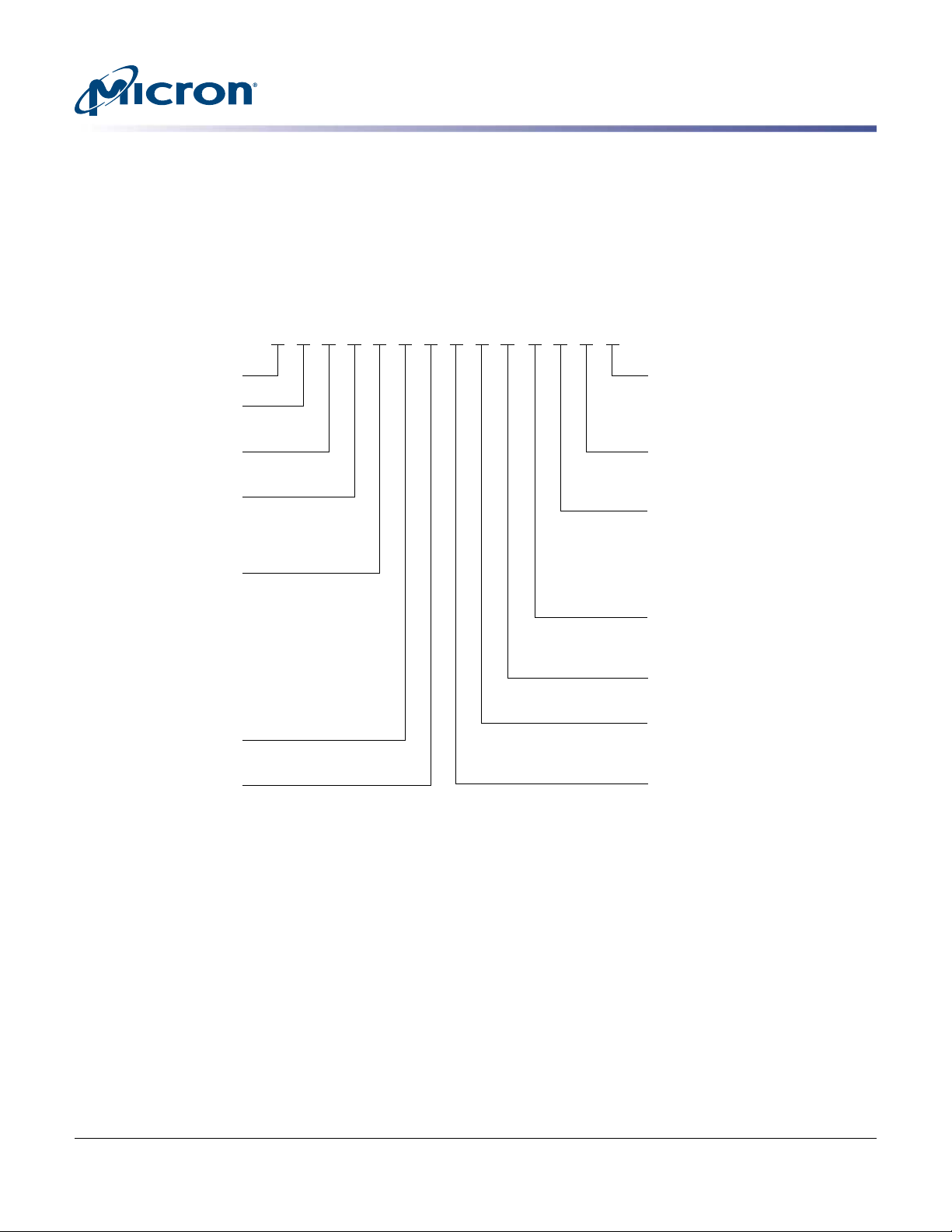
MT FD D AV 120 M AZ - 1 AE 1 ES
Micron Technology
Product Family
FD = Flash drive
Drive Interface
D = SATA 6.0 Gb/s
Drive Form Factor
AK = 2.5-inch (7mm)
AT = mSATA
AV = M.2 (80mm x 22mm 3.5mm)
Drive Density
064 = 64GB
120 = 120GB
128 = 128GB
240 = 240GB
256 = 256GB
480 = 480GB
512 = 512GB
960 = 960GB
1T0 = 1024GB
NAND Flash Type
M = MLC
Product Family
AV = M500
AY = M550
AZ = M510
Production Status
Blank = Production
ES = Engineering sample
MS = Mechanical sample
Customer Designator
YY = Standard
HA = HP (Client)
Feature Set
AA = Contact factory
AB = Standard
AC = Contact factory
ZZ = Blank
Z = Blank
Extended Feature Set
1 = Contact factory
2 = SED (self-encrypting drive)
Sector Size
1 = 512 byte
NAND Flash Component
AE = 128Gb, MLC, x8, 3.3V (20nm)
AH = 64Gb, MLC, x8, 3.3V (20nm)
BOM Revision
For example:
1 = 1st generation
2 = 2nd generation
2 AB HA
M500 2.5-Inch NAND Flash SSD
Features
Part Numbering Information
Micron’s M500 SSD is available in different configurations and densities. The chart below is a comprehensive list
of options for the M500 series devices; not all options listed can be combined to define an offered product. Visit
www.micron.com for a list of valid part numbers.
Figure 1: Part Number Chart
PDF: 09005aef84fed121
m500_2_5_ssd.pdf - Rev. G 8/14 EN
2
Micron Technology, Inc. reserves the right to change products or specifications without notice.
© 2013 Micron Technology, Inc. All rights reserved.
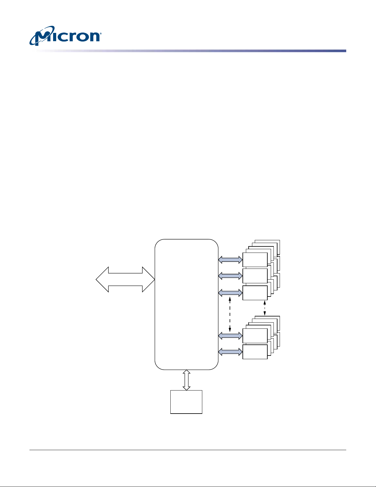
General Description
Micron’s solid state drive (SSD) uses a single-chip controller with a SATA interface on
the system side and 8-channels of Micron NAND Flash internally. Packaged in an HDD
replacement enclosure, the SSD integrates easily in existing storage infrastructures.
The SSD is designed to use the SATA interface efficiently during both READs and
WRITEs while delivering bandwidth-focused performance. SSD technology enables enhanced boot times, faster application load times, reduced power consumption, and extended reliability.
The self-encypting drive (SED) features a FIPS-compliant, AES-256 encryption engine,
providing hardware-based, secure data encryption, with no loss of SSD performance.
This SED follows the TCG/Opal specification for trusted peripherals.
When TCG/Opal features are not enabled, the device can perform alternate data encryption by invoking the ATA security command-set encryption features, to provide fulldisk encryption (FDE) managed in the host system BIOS. TCG/Opal and FDE feature
sets cannot be enabled simultaneously.
The data encryption is always running; however, encryption keys are not managed and
the data is not secure until either TCG/Opal or FDE feature sets are enabled.
M500 2.5-Inch NAND Flash SSD
General Description
Figure 2: Functional Block Diagram
SATA
SSD
controller
DRAM
buffer
NAND
NAND
NAND
NAND
NAND
PDF: 09005aef84fed121
m500_2_5_ssd.pdf - Rev. G 8/14 EN
3
Micron Technology, Inc. reserves the right to change products or specifications without notice.
© 2013 Micron Technology, Inc. All rights reserved.
M500 2.5-Inch NAND Flash SSD
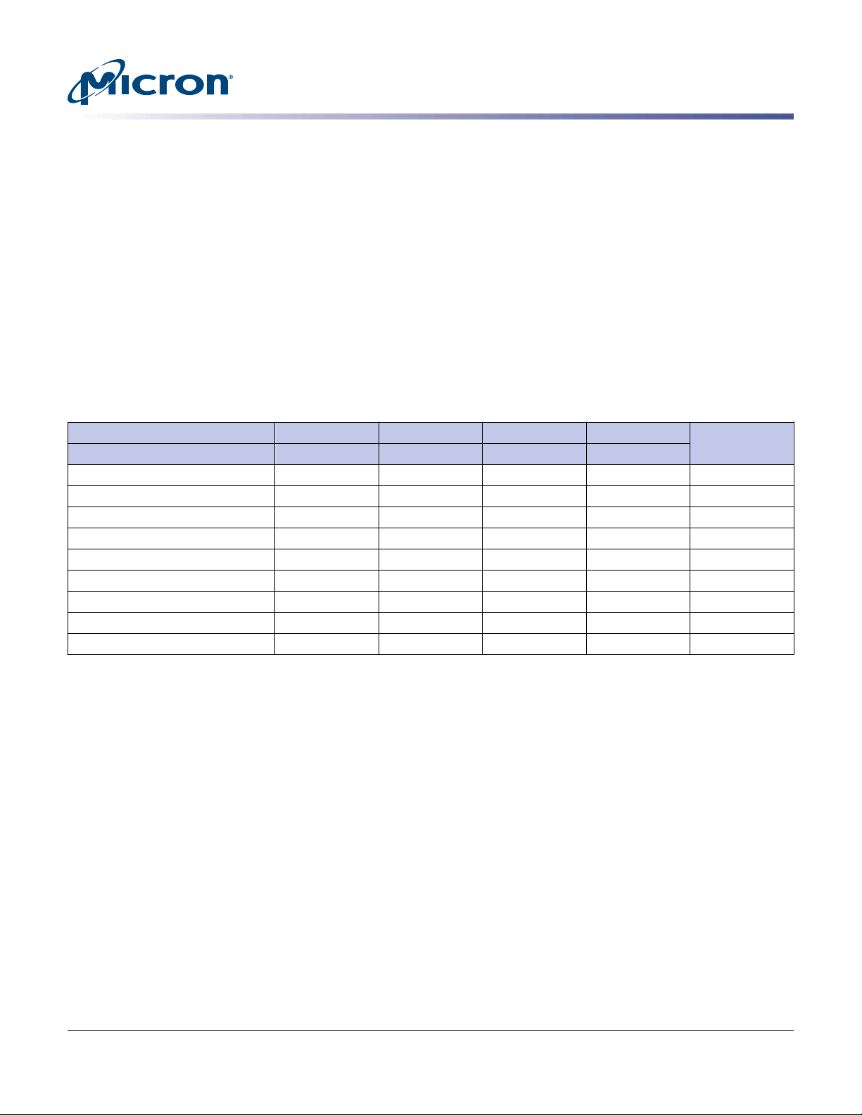
Logical Block Address Configuration
Logical Block Address Configuration
The drive is set to report the number of logical block addresses (LBA) that will ensure
sufficient storage space for the specified capacity. Standard LBA settings, based on the
IDEMA standard (LBA1-02), are shown below.
Table 1: Standard LBA Settings
User Available
Total LBA Max LBA
Capacity
120GB 234,441,648 DF94BB0 234,441,647 DF94BAF 120,034,123,776
240GB 468,862,128 1BF244B0 468,862,127 1BF244AF 240,057,409,536
480GB 937,703,088 37E436B0 937,703,087 37E436AF 480,103,981,056
960GB 1,875,385,008 6FC81AB0 1,875,385,007 6FC81AAF 960,197,124,096
Decimal Hexadecimal Decimal Hexadecimal (Unformatted)
Bytes
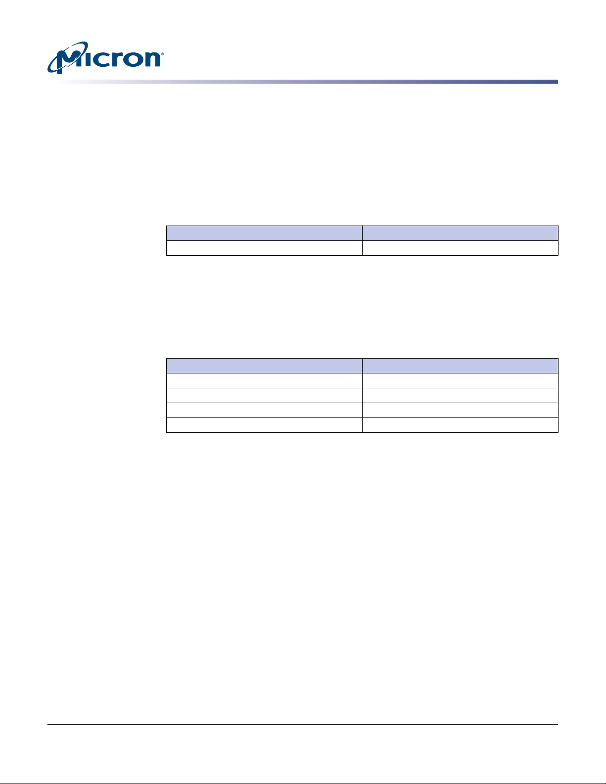
Physical Configuration
Table 2: 2.5-Inch Dimensions and Weight
Value
Specification
Height – 7.00 mm
Width 69.85 – mm
Length 100.45 – mm
Unit weight – 70 g
Insertion rating (cabled) 50 – insert/remove cycles
Insertion rating (backplane) 500 – insert/remove cycles
UnitNom Max
PDF: 09005aef84fed121
m500_2_5_ssd.pdf - Rev. G 8/14 EN
4
Micron Technology, Inc. reserves the right to change products or specifications without notice.
© 2013 Micron Technology, Inc. All rights reserved.
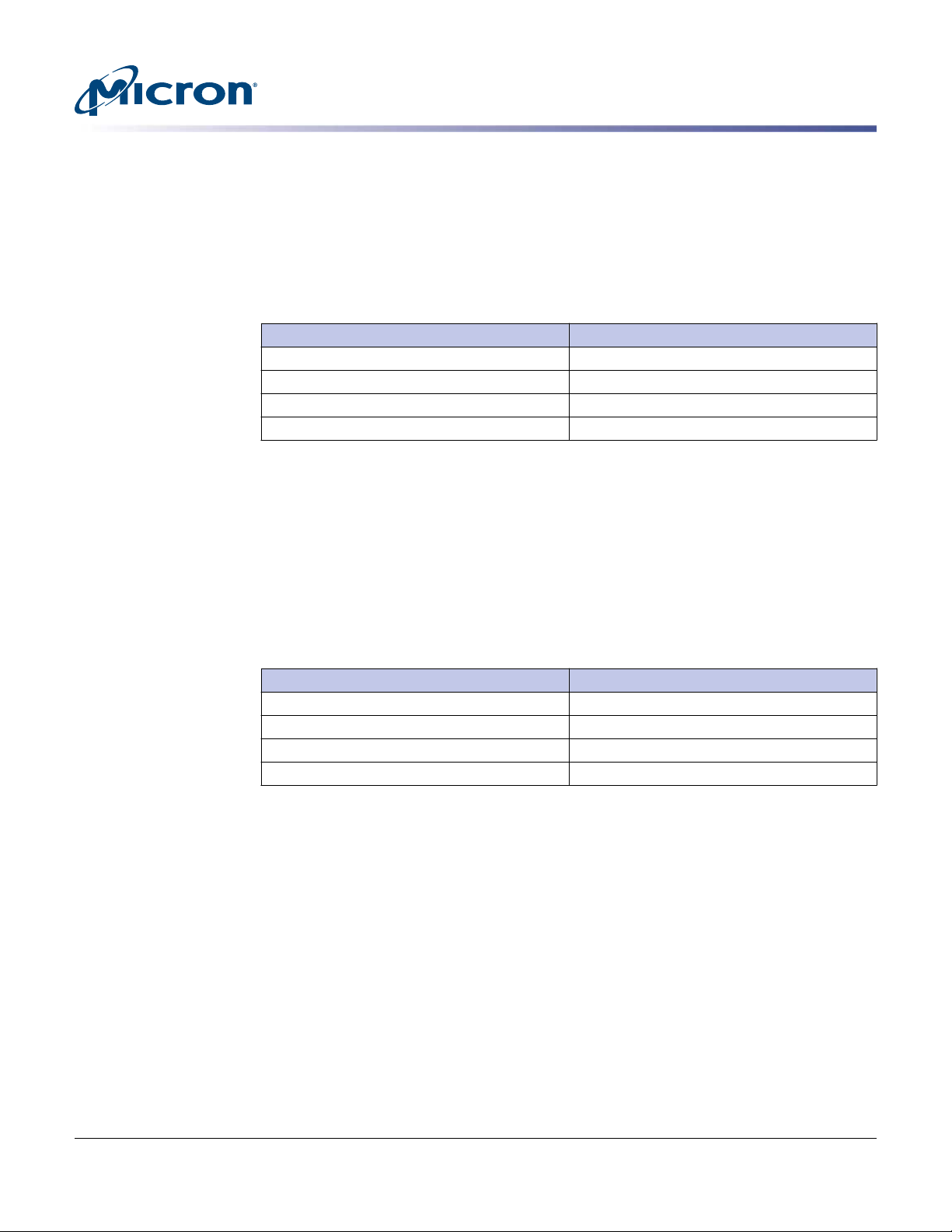
Interface Connectors
Power
segment
Signal
segment
P1
S1
The SATA signal segment interface cable has four conductors and three ground connections. As shown in Package Dimensions, the cable includes a 7-pin signal segment and a
15-pin power segment arranged in a single row with a 1.27mm (0.050in) pitch.
Figure 3: SSD Interface Connections
Table 3: SATA Signal Segment Pin Assignments
Signal Name Type Description
S1 GND Ground
S2 A
S3 A#
S4 GND Ground
S5 B#
S6 B
S7 GND Ground
M500 2.5-Inch NAND Flash SSD
Interface Connectors
Differential signal pair A and A#
Differential signal pair B and B#
Table 4: 2.5-Inch SATA Power Segment Pin Assignments
Pin# Signal Name Description
P1 RETIRED No connect
P2 RETIRED No connect
P3 DEVSLP Device sleep
P4 GND Ground
P5 GND Ground
P6 GND Ground
P7 V5 5V power, precharge
P8 V5 5V power
P9 V5 5V power
P10 GND Ground
P11 DAS Device activity signal
P12 GND Ground
P13 V12 No connect
P14 V12 No connect
P15 V12 No connect
PDF: 09005aef84fed121
m500_2_5_ssd.pdf - Rev. G 8/14 EN
5
Micron Technology, Inc. reserves the right to change products or specifications without notice.
© 2013 Micron Technology, Inc. All rights reserved.
M500 2.5-Inch NAND Flash SSD
Performance
Performance
Measured performance can vary for a number of reasons. The major factors affecting
drive performance are the capacity of the drive and the interface of the host. Additionally, overall system performance can affect the measured drive performance. When
comparing drives, it is recommended that all system variables are the same, and only
the drive being tested varies.
Performance numbers will vary depending on the host system configuration.
For SSDs designed for the client computing market, Micron specifies performance in
FOB ("fresh-out-of-box") state. Data throughput measured in "steady state" may be
lower than FOB state, depending on the nature of the data workload.
For a description of these performance states and of Micron's best practices for performance measurement, refer to micron.com/ssd.
Table 5: Drive Performance
Capacity 120GB 240GB 480GB 960GB
UnitInterface Speed 6 Gb/s 6 Gb/s 6 Gb/s 6 Gb/s
PCMark Vantage 70,000 80,000 80,000 80,000 HDD score
Sequential read (128KB transfer) 500 500 500 500 MB/s
Sequential write (128KB transfer) 130 250 400 400 MB/s
Random read (4KB transfer) 62,000 72,000 80,000 80,000 IOPS
Random write (4KB transfer) 35,000 60,000 80,000 80,000 IOPS
READ latency (MAX) 5 5 5 5 ms
WRITE latency (MAX) 25 25 25 25 ms
READ latency (TYP) 160 160 160 160 µs
WRITE latency (TYP) 40 40 40 40 µs
PDF: 09005aef84fed121
m500_2_5_ssd.pdf - Rev. G 8/14 EN
Notes:
1. Performance numbers are maximum values, except as noted.
2. Typical I/O performance numbers as measured using Iometer with a queue depth of 32
and write cache enabled. Fresh-out-of-box (FOB) state is assumed. For performance
measurement purposes, the SSD may be restored to FOB state using the secure erase
command.
3. Iometer measurements are performed on an 20GB span of logical block addresses
(LBAs).
4. 4KB transfers are used to measure READ/WRITE latency values with write cache enabled.
5. System variations will affect measured results. For comparison, PCMark scores are measured with the SSD as a secondary drive in a two-drive system. When measured as an OS
drive, system overhead can cause lower scores.
For a description of these performance states and of Micron's best practices for performance measurement, refer to Micron's technical marketing brief "Best Practices for
SSD Performance Measurement"
6
Micron Technology, Inc. reserves the right to change products or specifications without notice.
© 2013 Micron Technology, Inc. All rights reserved.
Reliability
Micron’s SSDs incorporate advanced technology for defect and error management.
They use various combinations of hardware-based error correction algorithms and
firmware-based static and dynamic wear-leveling algorithms.
Over the life of the SSD, uncorrectable errors may occur. An uncorrectable error is defined as data that is reported as successfully programmed to the SSD but when it is read
out of the SSD, the data differs from what was programmed.
Table 6: Uncorrectable Bit Error Rate
Uncorrectable Bit Error Rate Operation
<1 sector per 1015 bits read READ
Mean Time To Failure
Mean time to failure (MTTF) for the SSD can be predicted based on the component reliability data using the methods referenced in the Telcordia SR-332 reliability prediction
procedures for electronic equipment.
Table 7: MTTF
M500 2.5-Inch NAND Flash SSD
Reliability
Capacity MTTF (Operating Hours)
120GB 1.2 million
240GB 1.2 million
480GB 1.2 million
960GB 1.2 million
Note:
1. The product achieves a mean time to failure (MTTF) of 1.2 million hours, based on population statistics not relevant to individual units.
1
PDF: 09005aef84fed121
m500_2_5_ssd.pdf - Rev. G 8/14 EN
7
Micron Technology, Inc. reserves the right to change products or specifications without notice.
© 2013 Micron Technology, Inc. All rights reserved.
Endurance
M500 2.5-Inch NAND Flash SSD
Reliability
Endurance for the SSD can be predicted based on the usage conditions applied to the
device, the internal NAND component cycles, the write amplification factor, and the
wear-leveling efficiency of the drive. The tables below show the drive lifetime for each
SSD capacity by client computing and sequential input and based on predefined usage
conditions.
Table 8: Drive Lifetime – Client Computing
Capacity Drive Lifetime (Total Bytes Written)
120GB 72TB
240GB 72TB
480GB 72TB
960GB 72TB
Notes:
1. Total bytes written calculated with the drive 90% full.
2. SSD volatile write cache is enabled.
3. Access patterns used during reliability testing are 25% sequential and 75% random and
consist of the following: 50% are 4KiB; 40% are 64KiB; and 10% are 128KiB.
4. Host workload parameters, including write cache settings, IO alignment, transfer sizes,
randomness, and percent full, that are substantially different than the described notes,
may result in varied endurance results.
5. GB/day can be calculated by dividing the total bytes written value by (365 × number of
years). For example: 72TB/5 years/365 days = 40 GB/day for 5 years.
Table 9: Drive Lifetime – Sequential Input
Capacity Drive Lifetime (Total Bytes Written)
120GB 125TB
240GB 250TB
480GB 500TB
960GB 500TB
Notes:
1. Endurance of Client SSDs in some data center applications can be maximized by implementing workloads which are sequential when writing, with read-intensive access. Micron recommends no higher than 20% of input/output operations be writes.
2. SSD volatile write cache is enabled.
3. Micron recommends sequential writes in transfer sizes of 128KiB or integer multiples of
128KiB which are 4KiB-aligned. Contact Micron for details.
4. Host workload parameters, including write cache settings, IO alignment, transfer sizes,
randomness, and percent full, that are substantially different than the described notes,
may result in varied endurance results.
PDF: 09005aef84fed121
m500_2_5_ssd.pdf - Rev. G 8/14 EN
8
Micron Technology, Inc. reserves the right to change products or specifications without notice.
© 2013 Micron Technology, Inc. All rights reserved.
Electrical Characteristics
Environmental conditions beyond those listed may cause permanent damage to the device. This is a stress rating only, and functional operation of the device at these or any
other conditions above those indicated in the operational sections of this specification
is not implied. Exposure to absolute maximum rating conditions for extended periods
may affect reliability.
Table 10: SATA Power Consumption
M500 2.5-Inch NAND Flash SSD
Electrical Characteristics
Device Sleep
Capacity
120GB <5 80 150 2100 mW
240GB <5 95 150 3200 mW
480GB <10 100 150 3600 mW
960GB <20 100 150 3800 mW
Average Idle Average Active Average
Notes:
1. Data taken at 25°C using a 6 Gb/s SATA interface.
2. Active average power measured while running MobileMark Productivity Suite.
3. DIPM (device-initiated power management) enabled. DIPM Slumber supported.
4. Active maximum power is measured using Iometer with 128KB sequential write transfers.
Active Maximum
(128KB transfer) Unit
Table 11: Maximum Ratings
Parameter/Condition Symbol Min Max Unit
Voltage input V5 4.5 5.5 V
Operating temperature T
Non-operating temperature –40 85 °C
Rate of temperature change – 20 °C/hour
Relative humidity (non-condensing) 5 95 %
Notes:
1. Temperature is best measured by reading the SSD's on-board temperature sensor, which
is recorded in SMART attribute 194 (or 0xC2).
2. Power-off sequence: When the SSD is shut down, the ATA STANDBY IMMEDIATE (STBI)
command should be the last command sent by the host and acknowledged by the SSD.
Failure to follow this process might result in a longer than normal time-to-ready (TTR)
during the subsequent power-on sequence. TTR is the time from power-on to drive
ready to accept SATA commands.
S
0 70 °C
Table 12: Shock and Vibration
Parameter/Condition Specification
Non-operating shock 1500G/0.5ms
Non-operating vibration 5–800Hz @ 3.13G
PDF: 09005aef84fed121
m500_2_5_ssd.pdf - Rev. G 8/14 EN
9
Micron Technology, Inc. reserves the right to change products or specifications without notice.
© 2013 Micron Technology, Inc. All rights reserved.
Adaptive Thermal Monitoring
The device features adaptive thermal monitoring. While most host computers exhibit
operating environments that keep an SSD running in the range of 40°C to 45°C, adaptive thermal monitoring enables the SSD device to operate in a wide variety of environments by helping to prevent the host computer from running at excessive temperatures.
Adaptive thermal monitoring reduces NAND operations by approximately 40% when
the SSD's internal measured temperature reaches 75°C. The SSD remains in this lowered performance state until the temperature returns to 65°C; the SSD then returns to
normal operating mode. These transition points might occur at points somewhat different from case or ambient temperature because of thermal effects that cause a difference
between temperature sensed at the PCB level and temperature at the specified operating environment.
Adaptive thermal monitoring does not change the current negotiated speed of the SATA
bus, nor require or cause any new commands to be issued on the SATA bus. Ratedthroughput performance is not guaranteed at any point above the maximum specified
operating temperature.
The thermal monitoring feature can be disabled using ATA SET FEATURE commands as
described below. The default setting is ENABLED.
Note: The SSD will return to the default setting after each power cycle or COMRESET
command. Arrangements should be made to re-issue the DISABLE command after each
power cycle or COMRESET.
M500 2.5-Inch NAND Flash SSD
Adaptive Thermal Monitoring
DISABLE THERMAL MONITORING Command
• Command set feature
• Sub-command enable SATA feature
• Specific feature hardware feature control
• LBA FFFFh
• IDFY word 78, bit 5 will be set to indicate SATA hardware feature control is active
Table 13: Disable Thermal Monitoring Command Set Register
Register
Feature Set
Feature 10h
Sector count 08h
Sector number FFh
Cylinder low FFh
Cylinder high xx
Drive head xx
Command EFh
7 6 5 4 3 2 1 0
ENABLE THERMAL MONITORING Command
• Command set feature
• Sub-command disable SATA feature
PDF: 09005aef84fed121
m500_2_5_ssd.pdf - Rev. G 8/14 EN
10
Micron Technology, Inc. reserves the right to change products or specifications without notice.
© 2013 Micron Technology, Inc. All rights reserved.
• Specific feature hardware feature Control
• LBA FFFFh
• IDFY word 78, bit 5 will be set to indicate SATA hardware feature control is inactive
Table 14: Enable Thermal Monitoring Command Set Register
Register
Feature Set
Feature 0x90h
Sector count 0x8h
Sector number 0xFFh
Cylinder low 0xFFh
Cylinder high xx
Drive head xx
Command 0xEFh
7 6 5 4 3 2 1 0
M500 2.5-Inch NAND Flash SSD
Adaptive Thermal Monitoring
PDF: 09005aef84fed121
m500_2_5_ssd.pdf - Rev. G 8/14 EN
11
Micron Technology, Inc. reserves the right to change products or specifications without notice.
© 2013 Micron Technology, Inc. All rights reserved.
M500 2.5-Inch NAND Flash SSD
TCG/Opal Support
TCG/Opal Support
Table 15: TCG/Opal Support Parameters
Property Supported? Comments
TCG Storage Specifications
OPAL: TCG Storage Security SubSystem
Class
TCG Core Specification Specification 2.00 Revision 2.00, Nov 4, 2011
TCG Storage Interface Interactions Specification
OPAL SSC 1.00 (backward compatibility) Not supported –
OPAL SSC Additional Feature Set Specification
Additional DataStore Table Supported Specification 1.00 Revision 1.00, Feb 24, 2012
Single User Mode Supported Specification 1.00 Revision 1.00, Feb 24, 2012
TCG Storage Protection Mechanisms for
Secrets
PSID – Physical Presence SID Supported Specification Version 1.00 Committee Draft Revi-
GUDID (Globally Unique Serial Number) Supported Mandatory GUDID Proposal 11/03/2011 (Microsoft)
SID Authority Disable Supported SID Authority Disable Proposal 9/26/2011 (Micro-
Modifiable CommonName Columns Supported Modifiable CommonName Columns Proposal
OPAL SSC Feature Set – Specific List
ALL OPAL Mandatory Features Supported –
Close Session (optional) Supported Allows Tper to notify the host it has aborted a ses-
Restricted Command & Table (optional) Not Supported The interface control template enables TPer control
Type Table (not required) Not Supported –
Activate Method Supported –
Revert Method Supported –
Revert SP Method Supported –
Activate Method Within Transactions Not Supported As per OPAL, this behavior is out of the scope
Revert Method within Transactions Not Supported As per OPAL, this behavior is out of the scope
Revert SP Method within Transactions Not Supported As per OPAL, this behavior is out of the scope
Creation/Deletion of Tables/Rows after
Manufacturing
Tper Feature
COM ID Management Support Not Supported Dynamic COM ID allocation & management not
Buffer Management Support Not Supported Flow control
Specification 2.00 Revision 1.00, Feb 24, 2012
TCG Reference
Specification
Specification Version 1.02 Revision 1.00 30 December, 2011
Supported Specification Version 1.00 Revision 1.07 17 August,
2011
sion 1.05 February 9, 2011
soft)
7/22/2010 (Microsoft)
sion
over selected interface commands; the benefit is
the reduction of undesired side effects
Not Supported As per OPAL, this behavior is out of the scope
supported
PDF: 09005aef84fed121
m500_2_5_ssd.pdf - Rev. G 8/14 EN
12
Micron Technology, Inc. reserves the right to change products or specifications without notice.
© 2013 Micron Technology, Inc. All rights reserved.
 Loading...