

Micron MTFDDAK100MAN-1S1AA, MTFDDAK200MAN-1S1AA, MTFDDAK400MAN-1S1AA User Manual

P400m 2.5-Inch NAND Flash SSD
P400m 2.5-Inch SATA NAND Flash SSD
MTFDDAK100MAN-1S1AA, MTFDDAK200MAN-1S1AA,
MTFDDAK400MAN-1S1AA
Features
Features
• Micron® 25nm MLC NAND Flash
• RoHS-compliant package
• SATA 6 Gb/s interface
• ATA modes supported
– PIO mode 3, 4
– Multiword DMA mode 0, 1, 2
– Ultra DMA mode 0, 1, 2, 3, 4, 5
• Enterprise sector size support
– 512-byte
• Hot-plug capable
• Native command queuing support with 32-command slot support
• ATA-8 ACS2 command set compliant
• ATA security feature command set and password
login support
• Security erase command set: fast and secure erase
• Self-monitoring, analysis, and reporting technology
(SMART) command set
• 100GB performance (steady state)
– Sequential 64KB read: 380 MB/s
– Sequential 64KB write: 200 MB/s
– Random 4KB read: 52,000 IOPS
– Random 4KB write: 21,000 IOPS
– READ latency: 0.57ms
– WRITE latency: 2ms
• 200GB performance (steady state)
– Sequential 64KB read: 380 MB/s
– Sequential 64KB write: 310 MB/s
– Random 4KB read: 54,000 IOPS
– Random 4KB write: 26,000 IOPS
– READ latency: 0.51ms
– WRITE latency: 2ms
• 400GB performance (steady state)
– Sequential 64KB read: 380 MB/s
– Sequential 64KB write: 310 MB/s
– Random 4KB read: 60,000 IOPS
– Random 4KB write: 26,000 IOPS
– READ latency: 0.51ms
– WRITE latency: 2ms
1, 2
1, 2
1, 2
• Reliability
– Mean time to failure (MTTF): 2 million device
3
hours
– Static and dynamic wear leveling
– Uncorrectable bit error rate (UBER): <1 sector
per 1016 bits read
• Endurance: Total bytes written (TBW)
– 100GB: 1.75PB; 200GB: 3.50PB; 400GB: 7.00PB
• Capacity4 (unformatted): 100GB, 200GB, 400GB
• Mechanical: 7.0mm height
– SATA connector: 5V ±10%
– 2.5-inch drive: 100.5mm x 69.85mm x 7.0mm
• Field-upgradeable firmware
• Power consumption: <7.5W (TYP)
• Operating temperature
– Commercial (0°C to 70°C)
Notes:
1. Typical I/O performance numbers as measured using Iometer with a queue depth of
32 and write cache disabled.
2. 4KB transfers used for READ/WRITE latency
values.
3. The product achieves a MTTF based on population statistics not relevant to individual
units.
4. 1GB = 1 billion bytes; formatted capacity is
less.
5. Drive case temperature.
5
Warranty: Contact your Micron sales representative
for further information regarding the product,
including product warranties.
PDF: 09005aef84952553
p400m_2_5.pdf - Rev. H 11/13 EN
Products and specifications discussed herein are subject to change by Micron without notice.
1
Micron Technology, Inc. reserves the right to change products or specifications without notice.
© 2011 Micron Technology, Inc. All rights reserved.
MT FD D AK 100 M AN - 1 S 1
Micron Technology
Product Family
FD = Flash drive
Drive Interface
D = SATA 6.0 Gb/s
Drive Form Factor
AK = 2.5-inch (7.0mm)
Drive Density
100 = 100GB
200 = 200GB
400 = 400GB
NAND Flash Type
M = MLC
Product Family
AN = P400m
Production Status
Blank = Production
ES = Engineering sample
Operating Temperature Range
Blank = Commercial (0°C to 70°C)
Hardware Feature Set
Blank = Null
AA = Contact factory
AB = Contact factory
AC = Contact factory
BOM Revision
1 = 1st generation
NAND Flash Component
S = 42Gb, MLC, x8 3.3V (25nm)
Sector Size
1 = 512-byte
ESAA
P400m 2.5-Inch NAND Flash SSD
Features
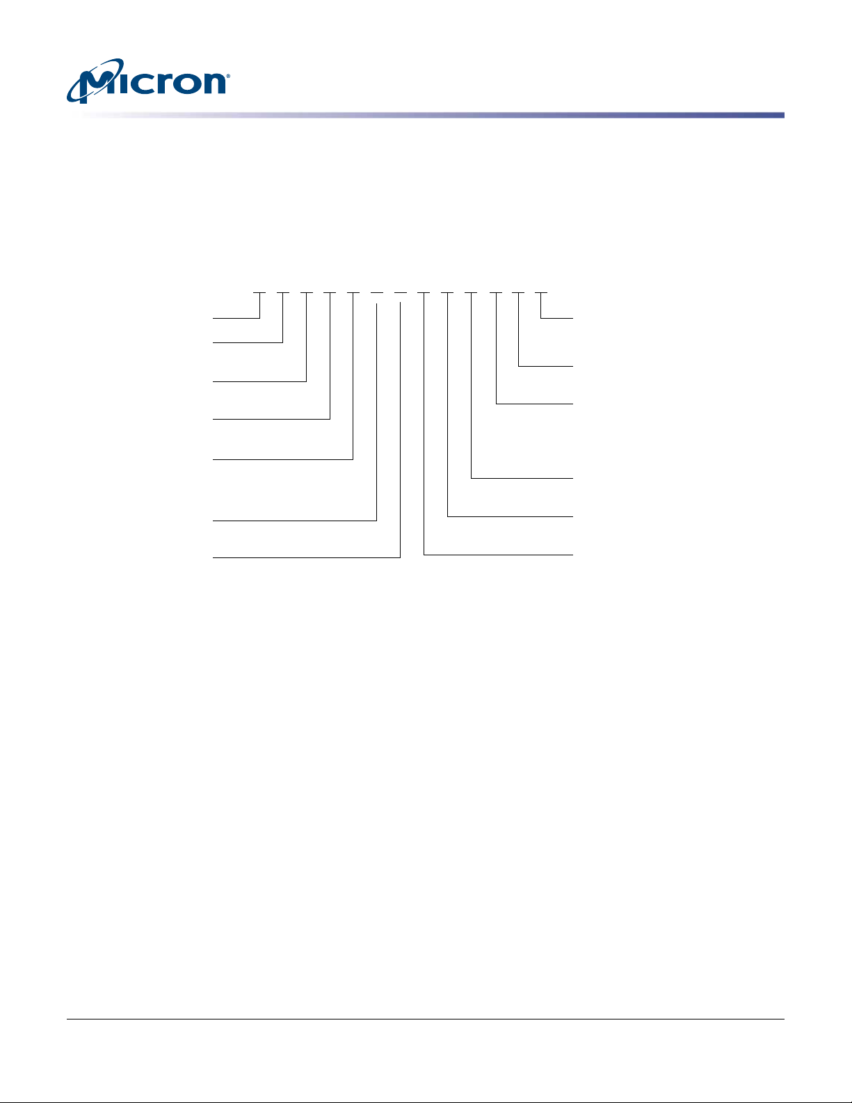
Part Numbering Information
Micron’s P400m SSD is available in different configurations and densities. Visit micron.com for a list of valid part
numbers.
Figure 1: Part Number Chart
PDF: 09005aef84952553
p400m_2_5.pdf - Rev. H 11/13 EN
2
Micron Technology, Inc. reserves the right to change products or specifications without notice.
© 2011 Micron Technology, Inc. All rights reserved.
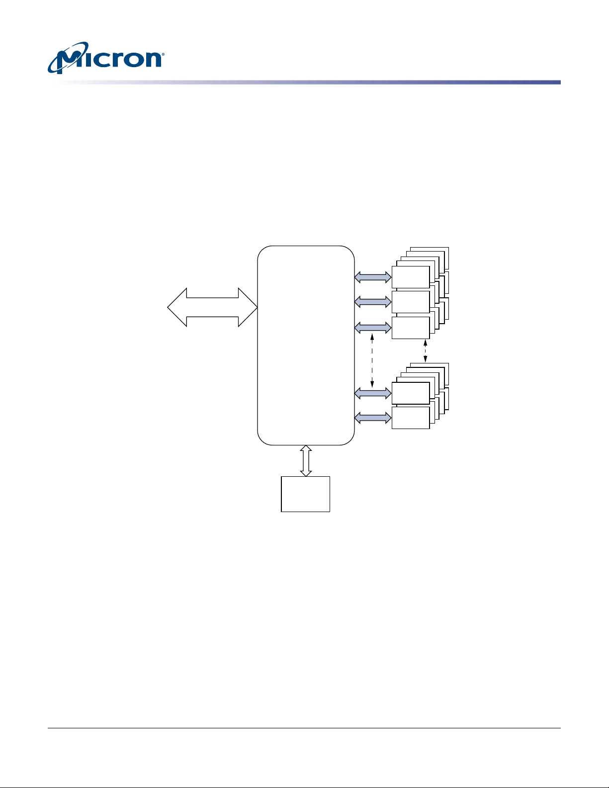
General Description
Micron’s P400m solid state drive (SSD) uses a single-chip controller with a SATA interface on the system side and n-channels of Micron NAND Flash internally. Packaged in
an HDD replacement enclosure, the SSD integrates easily in existing storage infrastructures.
The P400m SSD is designed to support and manage the needs of enterprise platforms
that utilize significant read/write mixed workloads. Optimized to support enterprise
needs previously supported solely by SLC solutions, the P400m will provide the endurance and data integrity required by these growing environments.
Figure 2: Functional Block Diagram
P400m 2.5-Inch NAND Flash SSD
General Description
NAND
SATA
SSD
controller
DRAM
buffer
NAND
NAND
NAND
NAND
PDF: 09005aef84952553
p400m_2_5.pdf - Rev. H 11/13 EN
3
Micron Technology, Inc. reserves the right to change products or specifications without notice.
© 2011 Micron Technology, Inc. All rights reserved.
P400m 2.5-Inch NAND Flash SSD
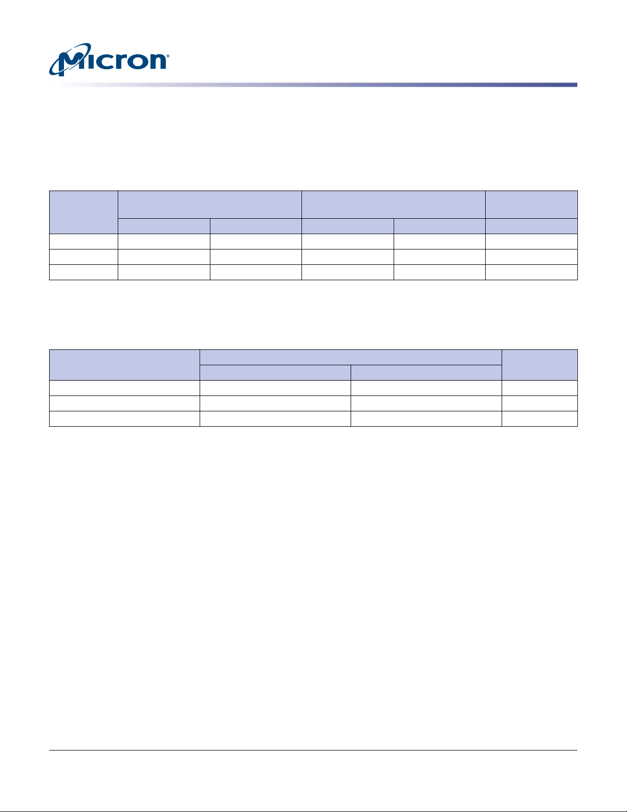
Logical Block Address Configuration
Logical Block Address Configuration
The drive is set to report the number of logical block addresses (LBA) that will ensure
sufficient storage space for the specified density. Standard LBA settings, based on the
IDEMA standard (LBA1-02), are shown below.
Table 1: Standard LBA Settings – 512-Byte Sector Size
User Available
Total LBA Max LBA
Drive Size
100GB 195,371,568 BA52230 195,371,567 BA5222F 100,030,242,816
200GB 390,721,968 1749F1B0 390,721,967 1749F1AF 200,049,647,616
400GB 781,422,768 2E9390B0 781,422,767 2E9390AF 400,088,457,216
Decimal Hexadecimal Decimal Hexadecimal (Unformatted)
Bytes
Physical Configuration
Table 2: 2.5-Inch Dimensions
Value
Specification
Height – 7.0 mm
Width 69.85 – mm
Length 100.50 – mm
UnitNom Max
PDF: 09005aef84952553
p400m_2_5.pdf - Rev. H 11/13 EN
4
Micron Technology, Inc. reserves the right to change products or specifications without notice.
© 2011 Micron Technology, Inc. All rights reserved.
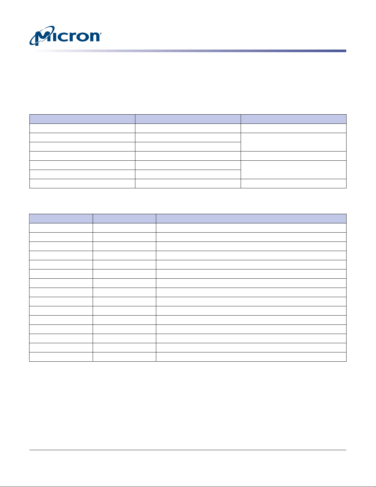
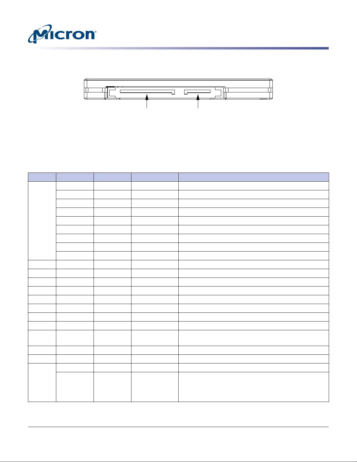
Interface Connectors
The SATA signal segment interface cable has four conductors and three ground connections. As shown in Package Dimensions, the cable includes a 7-pin signal segment and a
15-pin power segment arranged in a single row with a 1.27mm (0.050in) pitch.
Table 3: SATA Signal Segment Pin Assignments
Signal Name Type Description
S1 GND Ground
S2 A
S3 A#
S4 GND Ground
S5 B#
S6 B
S7 GND Ground
Table 4: 2.5-Inch SATA Power Segment Pin Assignments
P400m 2.5-Inch NAND Flash SSD
Interface Connectors
Differential signal pair A and A#
Differential signal pair B and B#
Pin# Signal Name Description
P1 V33 No connect
P2 V33 No connect
P3 V33 No connect
P4 GND Ground
P5 GND Ground
P6 GND Ground
P7 V5 5V power, precharge
P8 V5 5V power
P9 V5 5V power
P10 GND Ground
P11 DAS Device activity signal
P12 GND Ground
P13 V12 No connect
P14 V12 No connect
P15 V12 No connect
PDF: 09005aef84952553
p400m_2_5.pdf - Rev. H 11/13 EN
5
Micron Technology, Inc. reserves the right to change products or specifications without notice.
© 2011 Micron Technology, Inc. All rights reserved.
Power
segment
P1 S1
Signal
segment
P400m 2.5-Inch NAND Flash SSD
Figure 3: SSD Interface Connections
Device ID
Table 5: Identify Device
See Note 1 for setting definitions
Word Bit(s) Setting Default Value Description
0 – – – General configuration bit-significant information
15 F 0b 0 = ATA device
14–8 X 00000000 Retired
7 F 0b 1 = Removable media device
6 F 1b Obsolete
5–3 X 000b Retired
2 V 0b Response incomplete
1 X 0b Retired
0 F 0b Reserved
1 – – 3FFFh Obsolete
2 – F C837h Specific configuration
3 – F 0010h Obsolete
4 – F 0000h 0000h Retired
6 – F 003Fh Obsolete
7 – (O)V 0000h 0000h
9 – ( )X 0000h Retired
10 – (M)F Varies Serial number (20 ASCII characters)
20 – ( )X 0000h 0000h
0000h
23 – (M)F Varies Firmware revision (8 ASCII characters)
27 – (M)F Varies Model number (40 ASCII characters)
47 15–8 F 80h 80h
7–0 F 10h 00h = Reserved
Reserved for assignment by the CompactFlash™ Association
Retired/obsolete
01h-FFh = Maximum number of logical sectors that shall be
transferred per DRQ data block on READ/WRITE MULTIPLE
commands
Device ID
PDF: 09005aef84952553
p400m_2_5.pdf - Rev. H 11/13 EN
6
Micron Technology, Inc. reserves the right to change products or specifications without notice.
© 2011 Micron Technology, Inc. All rights reserved.
P400m 2.5-Inch NAND Flash SSD
Table 5: Identify Device (Continued)
See Note 1 for setting definitions
Word Bit(s) Setting Default Value Description
48 – – – Trusted Computing feature set options
15 F 0b Shall be cleared to zero
14 F 1b Shall be set to one
13–1 F 0000000000000b Reserved for the Trusted Computing Group
0 F 0b 1 = Trusted Computing feature set is supported
49 – – – Capabilities
15–14 F 00b Reserved for the IDENTIFY PACKET DEVICE command
13 F 1b 1 = Standby timer values as specified in this standard are
supported
– – – 0 = Standby timer values shall be managed by the device
12 F 0b Reserved for the IDENTIFY PACKET DEVICE command
11 F 1b 1 = IORDY is supported
– – – 0 = IORDY may be supported
10 F 1b 1 = IORDY may be disabled
9 – 1b 1 = LBA is supported
8 F 1b 1 = DMA is supported
7–0 F 00000000b Retired
50 – – – Capabilities
15 F 0b Shall be cleared to zero
14 F 1b Shall be set to one
13–2 F 000000000000b Reserved
1 X 0b Obsolete
0 F 1b Shall be set to one to indicate a vendor-specific standby tim-
er value minimum
51 – ( )X 0000h 0000h Obsolete
53 15–3 F 0000000000000b Reserved
2 F 1b 1 = The fields reported in word 88 are valid
0 = The fields reported in word 88 are not valid
1 F 1b 1 = The fields reported in words (70:64) are valid
0 = the fields reported in words (70:64) are not valid
0 X 1b Obsolete
54 – ( )X 3FFFh 0010h
003Fh FC10h
00FBh
Obsolete
Device ID
PDF: 09005aef84952553
p400m_2_5.pdf - Rev. H 11/13 EN
7
Micron Technology, Inc. reserves the right to change products or specifications without notice.
© 2011 Micron Technology, Inc. All rights reserved.
P400m 2.5-Inch NAND Flash SSD
Device ID
Table 5: Identify Device (Continued)
See Note 1 for setting definitions
Word Bit(s) Setting Default Value Description
59 15 F 1b 1 = The BLOCK ERASE EXT command is supported
14 F 1b 1 = The OVERWRITE EXT command is supported
13 F 0b 1 = The CRYPTO SCRAMBLE EXT command is supported
12 F 1b 1 = The sanitize feature set is supported
11–9 F 000b Reserved
8 V 1b 1 = Multiple sector settings are valid
7–0 V 00010000b xxh = Current setting for number of logical sectors that shall
be transferred per DRQ data block on READ/WRITE MULTIPLE commands
60 – M(F) Varies by capacity Total number of user addressable logical sectors
62 – ( )X 0000h Obsolete
63 15–11 F 00000b Reserved
10 V 0b 1 = Multiword DMA mode 2 is selected
0 = Multiword DMA mode 2 is not selected
9 V 0b 1 = Multiword DMA mode 1 is selected
0 = Multiword DMA mode 1 is not selected
8 V 0b 1 = Multiword DMA mode 0 is selected
0 = Multiword DMA mode 0 is not selected
7–3 F 0000b Reserved
2 F 1b 1 = Multiword DMA mode 2 and below are supported
1 F 1b 1 = Multiword DMA mode 1 and below are supported
0 F 1b 1 = Multiword DMA mode 0 is supported
64 15–8 F 00h Reserved
7–0 F 03h PIO modes is supported
65 – F 0078h Minimum Multiword DMA transfer cycle time per word
Cycle time in nanoseconds
66 – F 0078h Manufacturer's recommended Multiword DMA transfer cy-
cle time
Cycle time in nanoseconds
67 – F 0078h Minimum PIO transfer cycle time without flow control
Cycle time in nanoseconds
68 – F 0078h Minimum PIO transfer cycle time with IORDY flow control
Cycle time in nanoseconds
PDF: 09005aef84952553
p400m_2_5.pdf - Rev. H 11/13 EN
8
Micron Technology, Inc. reserves the right to change products or specifications without notice.
© 2011 Micron Technology, Inc. All rights reserved.
Table 5: Identify Device (Continued)
See Note 1 for setting definitions
Word Bit(s) Setting Default Value Description
69 – F – Additional supported
15 F 0b 1 = CFast specification is supported
14 F 1b 1 = Deterministic read after trim is supported
13 F 0b 1 = Long physical sector alignment error reporting control is
supported
12 F 0b 1 = DEVICE CONFIGURATION IDENTIFY DMA and DEVICE
CONFIGURATION SET DMA are supported
11 F 0b 1 = READ BUFFER DMA is supported
10 F 0b 1 = WRITE BUFFER DMA is supported
9 F 0b 1 = SET MAX PASSWORD DMA and SET MAX UNLOCK DMA
are supported
8 F 0b 1 = DOWNLOAD MICROCODE DMA is supported
7 F 0b Reserved for IEEE-1667
6 F 0b 1 = Optional ATA device 28-bit commands are supported
5 F 0b 1 = Read zero after trim is supported
4–0 F 00000b Reserved
70 – F 0000h Reserved
71 – F 0000h 0000h
0000h 0000h
75 – – – Queue depth
15–5 F 00000000000b Reserved
4–0 F 11111b Maximum queue depth - 1
76 – – – Serial ATA capabilities
15–13 F 000b Reserved
12 F 1b Native command queuing priority information is supported
11 F 0b Unload while NCQ commands are outstanding is supported
10 F 1b Physical event counters are supported
9 F 1b Receipt of host-initiated interface power management re-
8 F 1b Native command queuing is supported
7–4 F 0000b Reserved for future Serial ATA signaling speed grades
3 F 1b 1 = Serial ATA Gen-3 speed (6.0 Gb/s) is supported
2 F 1b 1 = Serial ATA Gen-2 speed (3.0 Gb/s) is supported
1 F 1b 1 = Serial ATA Gen-1 speed (1.5 Gb/s) is supported
0 F 0b Reserved (set to 0)
Reserved for the IDENTIFY PACKET DEVICE command
quests is supported
P400m 2.5-Inch NAND Flash SSD
Device ID
PDF: 09005aef84952553
p400m_2_5.pdf - Rev. H 11/13 EN
9
Micron Technology, Inc. reserves the right to change products or specifications without notice.
© 2011 Micron Technology, Inc. All rights reserved.
 Loading...