

Page 1

5100 Series NAND Flash SSD
5100 Series SATA NAND Flash SSD
MTFDDAK240T, MTFDDAK480T, MTFDDAK960T,
MTFDDAK1T9T, MTFDDAK3T8T, MTFDDAK7T6T
MTFDDAV240T, MTFDDAV480T, MTFDDAV960T,
MTFDDAV1T9T
Features
Features
• Micron® 3D TLC NAND Flash
• Three performance/endurance levels
– ECO
– PRO
– MAX
• TCG Enterprise compliant self-encrypting drive
(SED)
• FIPS 140-2 level 2 validation option available on
specific configurations
• SATA 6 Gb/s interface
• ATA modes supported
– PIO mode 3, 4
– Multiword DMA mode 0, 1, 2
– Ultra DMA mode 0, 1, 2, 3, 4, 5, 6
• 512-byte sector size support
• Hot-plug capable (2.5-inch only)
• Native command queuing support with 32-command slot support
• ATA-8 ACS-3 revision 5 command set compliant
• ATA security feature command set and password
login support
• Security erase command set: fast and secure erase
• Performance (steady state)
– Sequential 128KB read: Up to 540 MB/s
– Sequential 128KB write: Up to 520 MB/s
– Random 4KB read: Up to 93,000 IOPS
– Random 4KB write: Up to 74,000 IOPS
• Quality of Service
2
– Read/Write (99.9%): 500µs/500µs
– Read/Write (99.999%): 9ms/5ms
• Endurance4: Total bytes written (TBW)
– ECO: Up to 8,400TB
– PRO: Up to 17,600TB
– MAX: Up to 17,600TB
1
• Reliability
– MTTF: 2.0 million device hours
3
– Static and dynamic wear leveling
– Uncorrectable bit error rate (UBER): <1 sector
per 1017 bits read
– End-to-end data protection
– Enhanced power-loss data protection with data
protection capacitor monitoring
• Self-monitoring, analysis, and reporting technology
(SMART) command set
• Capacity4 (unformatted): 240GB, 480GB, 960GB,
1920GB, 3840GB, 7680GB
• Mechanical:
– 2.5-inch x 7.0mm form factor
– M.2 Type 2280 form factor
• RoHS-compliant package
• Secure field-upgradeable firmware with digitally
signed firmware image
• Power consumption: 240GB/480GB: <4.5W(TYP);
960GB: <5.0W(TYP); 1920GB: <5.5W(TYP); 3840GB/
7680GB: <6.0W(TYP)
• Operating temperature
– Commercial (0°C to 70°C)
Notes:
1. Performance varies by capacity and endurance.
2. 4KB transfers QD = 1 used for READ/WRITE
latency values.
3. The product achieves a MTTF based on population statistics not relevant to individual
units.
4. 1GB = 1 billion bytes; formatted capacity is
less.
5. As reported by SMART.
5
Warranty: Contact your Micron sales representative
for further information regarding the product,
including product warranties.
CCMTD-1725822587-10309
5100_series_SSD_disti.pdf - Rev. A 12/16 EN
Products and specifications discussed herein are subject to change by Micron without notice.
1
Micron Technology, Inc. reserves the right to change products or specifications without notice.
© 2016 Micron Technology, Inc. All rights reserved.
Page 2
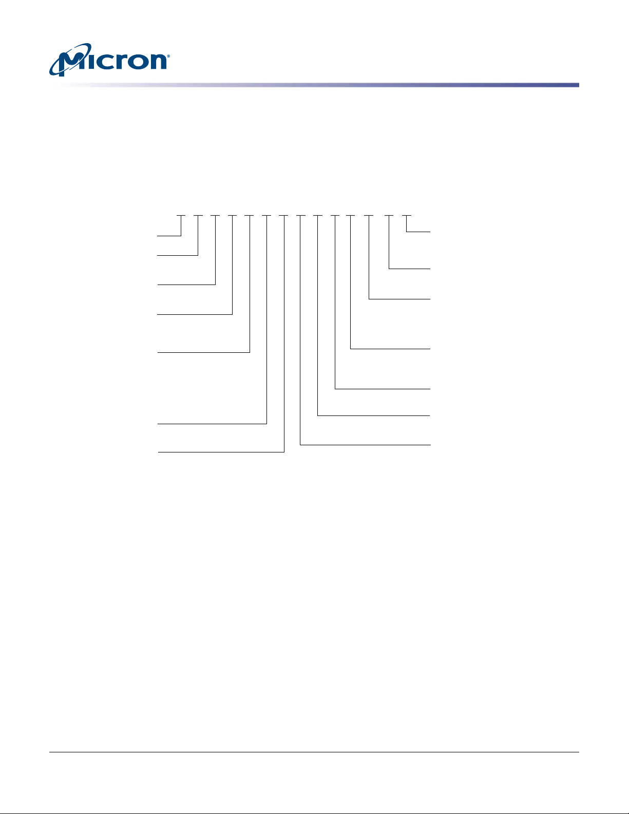
MT FD D AK 480 T BY - 1 AR 1 ES
Micron Technology
Product Family
FD = Flash drive
Drive Interface
D = SATA 6.0 Gb/s
Drive Form Factor
AK = 2.5-inch (7mm)
AV = M.2 (80mm x 22mm)
Drive Capacity
240 = 240GB
480 = 480GB
960 = 960GB
NAND Flash Type
T = TLC
Product Family
BY = 5100 ECO
CB = 5100 PRO
CC = 5100 MAX
Production Status
Blank = Production
ES = Engineering sample
Customer Designator
YY = Standard
Hardware Features
AB = Standard
FC = FIPS140-2 validated
TA = TAA Compliant
Extended Firmware Features
Z = None
6 = SED TCG eSSC
Sector Size
1 = 512 byte
NAND Flash Component
AR = 384Gb, TLC, x16, 1.8V (3D)
BOM Revision
For example:
1 = 1st generation
2 = 2nd generation
AB6 YY
7T6 = 7680GB
3T8 = 3840GB
1T9 = 1920GB
5100 Series NAND Flash SSD
Features
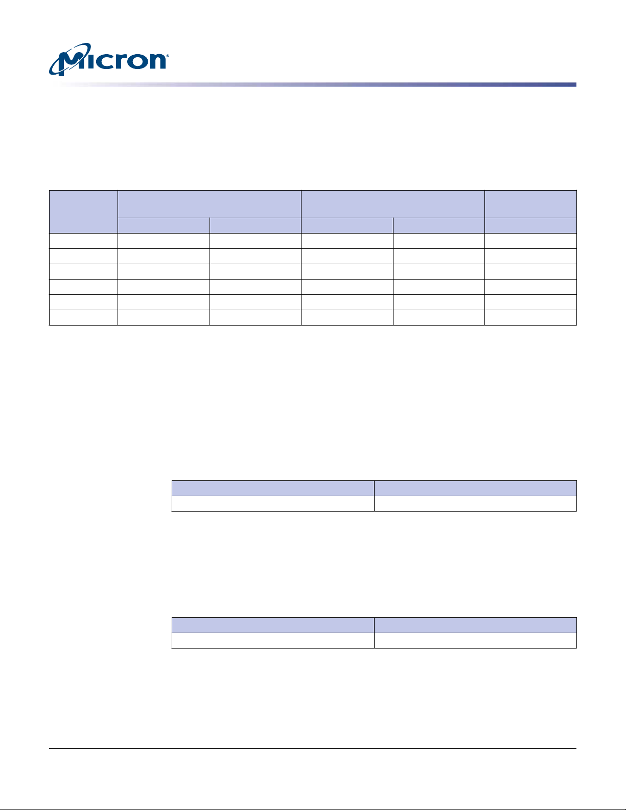
Part Numbering Information
Micron’s 5100 SSD is available in different configurations and densities. The chart below is a comprehensive list of
options for the 5100 series devices; not all options listed can be combined to define an offered product. Visit micron.com for a list of valid part numbers.
Figure 1: Part Number Chart
CCMTD-1725822587-10309
5100_series_SSD_disti.pdf - Rev. A 12/16 EN
2
Micron Technology, Inc. reserves the right to change products or specifications without notice.
© 2016 Micron Technology, Inc. All rights reserved.
Page 3
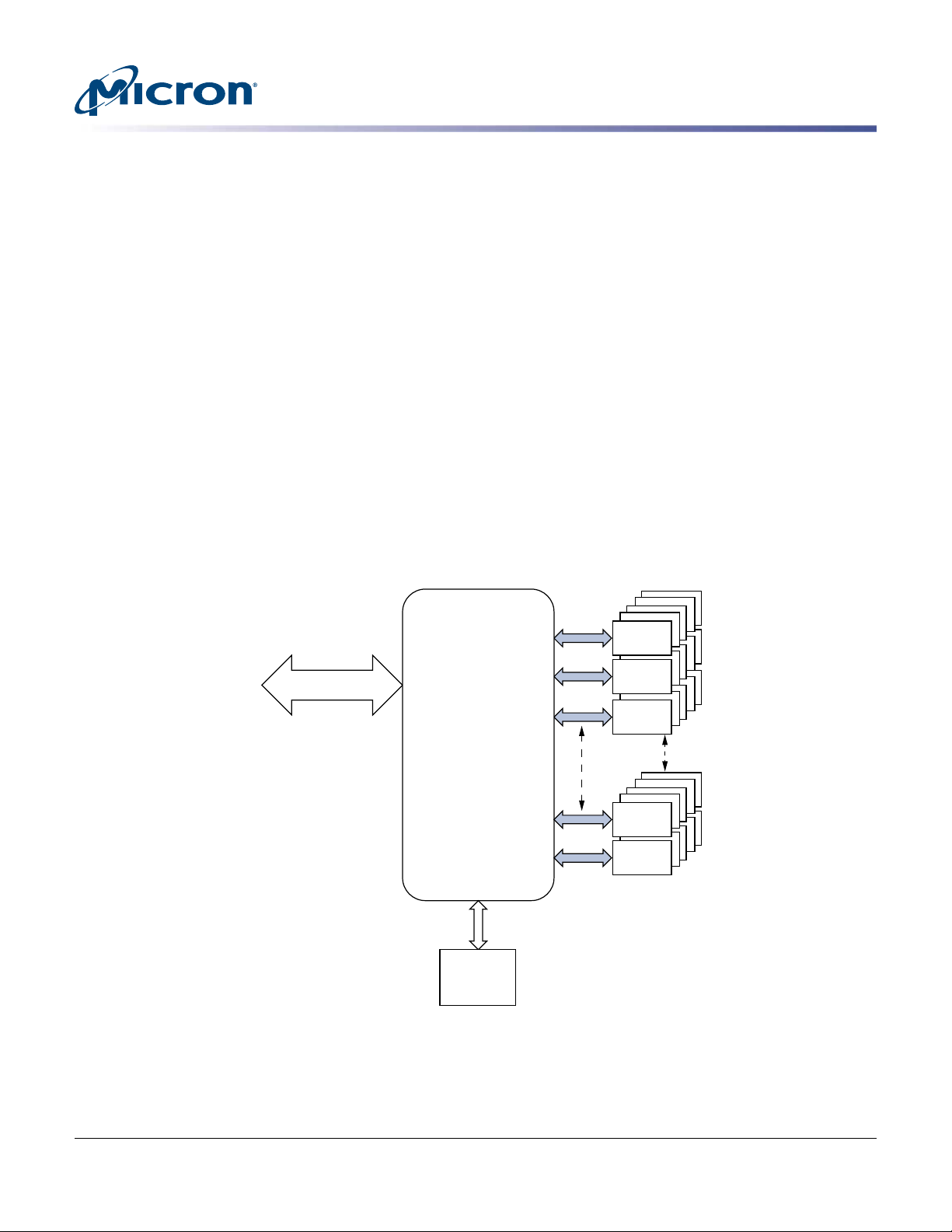
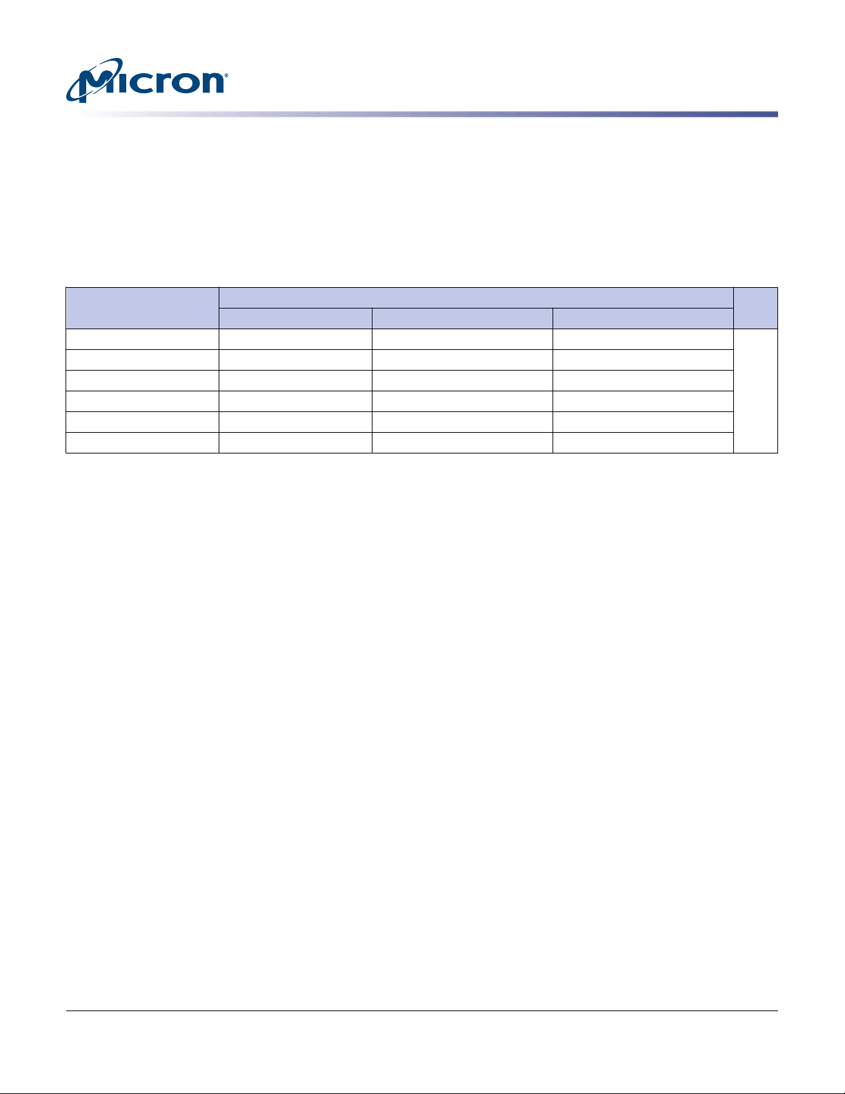
General Description
Micron’s 5100 solid state drive (SSD) uses a single-chip controller with a SATA interface
on the system side and four channels of Micron NAND Flash internally. Available in
both M.2 and 2.5-inch form factors, the SSD integrates easily in existing storage infrastructures.
The SSD is designed to use the SATA interface efficiently during both READs and
WRITEs while delivering bandwidth-focused performance. SSD technology enables enhanced boot times, faster application load times, reduced power consumption and extended reliability.
The self-encrypting drive (SED) features a FIPS validated, AES-256 encryption engine,
providing hardware-based, secure data encryption, with no loss of SSD performance.
This SED follows the TCG Enterprise specification for trusted peripherals. When TCG
Enterprise features are not enabled, the device can perform alternate data encryption
by invoking the ATA security command set encryption features, to provide full disk encryption (FDE) managed in the host system BIOS. TCG Enterprise and ATA security feature sets cannot be enabled simultaneously.
The data encryption is always running; however, encryption keys are not managed and
the data is not secure until either TCG Enterprise or ATA security feature sets are enabled.
5100 Series NAND Flash SSD
General Description
Figure 2: Functional Block Diagram
SATA
SSD
controller
DRAM
buffer
NAND
NAND
NAND
NAND
NAND
CCMTD-1725822587-10309
5100_series_SSD_disti.pdf - Rev. A 12/16 EN
3
Micron Technology, Inc. reserves the right to change products or specifications without notice.
© 2016 Micron Technology, Inc. All rights reserved.
Page 4
5100 Series NAND Flash SSD
Performance
Performance
Measured performance can vary for a number of reasons. The major factors affecting
drive performance are the capacity of the drive and the interface of the host. Additionally, overall system performance can affect the measured drive performance. When
comparing drives, it is recommended that all system variables are the same, and only
the drive being tested varies.
Performance numbers will vary depending on the host system configuration.
Table 1: Drive Performance – ECO
Capacity
Parameter
Sequential read (128KB transfer) 540 540 540 540 540 MB/s
Sequential write (128KB transfer) 380 520 520 520 520 MB/s
Random read (4KB transfer) 93,000 93,000 93,000 93,000 93,000 IOPS
Random write (4KB transfer) 31,000 28,000 24,000 18,000 9000 IOPS
Random 70/30 R/W (4KB transfer) 49,000 47,000 43,000 36,000 21,000 IOPS
READ latency (99.9%) 500 500 500 500 500 µs
WRITE latency (99.9%) 500 500 500 500 500 µs
READ latency (99.999%) 9.0 9.0 9.0 9.0 9.0 ms
WRITE latency (99.999%) 5.0 5.0 5.0 5.0 5.0 ms
Unit480GB 960GB 1920GB 3840GB 7680GB
Notes:
1. Typical I/O performance numbers as measured using fio with a queue depth of 32.
2. Fio measurements are performed in the steady state region.
3. 4KB transfers with a queue depth of 1 are used to measure READ/WRITE latency values.
4. System variations may affect measured results.
Table 2: Drive Performance – PRO
Capacity
Parameter
Sequential read (128KB transfer) 540 540 540 540 540 MB/s
Sequential write (128KB transfer) 250 410 520 520 520 MB/s
Random read (4KB transfer) 78,000 93,000 93,000 93,000 93,000 IOPS
Random write (4KB transfer) 26,000 43,000 37,000 38,000 36,000 IOPS
Random 70/30 R/W (4KB transfer) 43,000 55,000 54,000 57,000 54,000 IOPS
READ latency (99.9%) 500 500 500 500 500 µs
WRITE latency (99.9%) 500 500 500 500 500 µs
READ latency (99.999%) 9.0 9.0 9.0 9.0 9.0 ms
WRITE latency (99.999%) 5.0 5.0 5.0 5.0 5.0 ms
Notes:
1. Typical I/O performance numbers as measured using fio with a queue depth of 32.
2. Fio measurements are performed in the steady state region.
3. 4KB transfers with a queue depth of 1 are used to measure READ/WRITE latency values.
4. System variations may affect measured results.
Unit240GB 480GB 960GB 1920GB 3840GB
CCMTD-1725822587-10309
5100_series_SSD_disti.pdf - Rev. A 12/16 EN
4
Micron Technology, Inc. reserves the right to change products or specifications without notice.
© 2016 Micron Technology, Inc. All rights reserved.
Page 5
5100 Series NAND Flash SSD
Performance
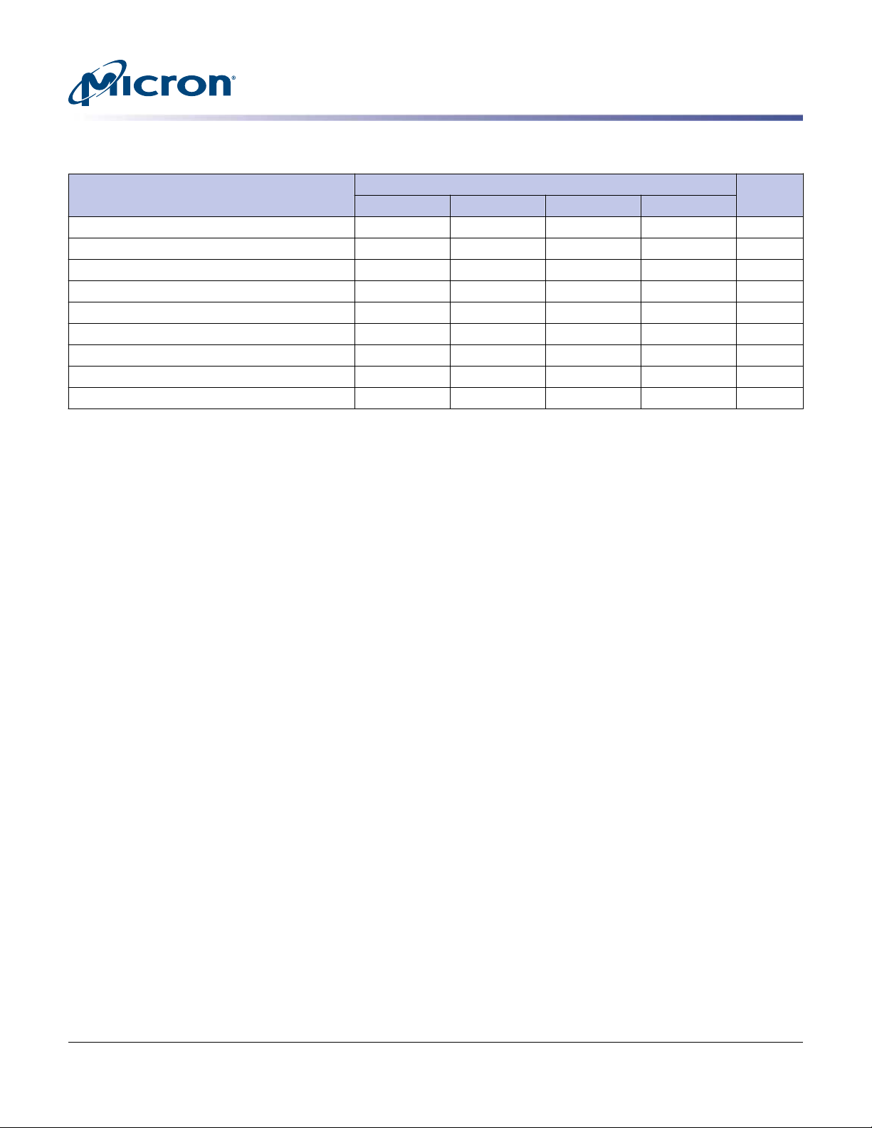
Table 3: Drive Performance – MAX
Capacity
Parameter
Sequential read (128KB transfer) 540 540 540 540 MB/s
Sequential write (128KB transfer) 310 460 520 520 MB/s
Random read (4KB transfer) 93,000 93,000 93,000 93,000 IOPS
Random write (4KB transfer) 48,000 74,000 74,000 66,000 IOPS
Random 70/30 R/W (4KB transfer) 57,000 70,000 72,000 70,000 IOPS
READ latency (99.9%) 500 500 500 500 µs
WRITE latency (99.9%) 500 500 500 500 µs
READ latency (99.999%) 9.0 9.0 9.0 9.0 ms
WRITE latency (99.999%) 5.0 5.0 5.0 5.0 ms
Unit240GB 480GB 960GB 1920GB
Notes:
1. Typical I/O performance numbers as measured using fio with a queue depth of 32.
2. Fio measurements are performed in the steady state region.
3. 4KB transfers with a queue depth of 1 are used to measure READ/WRITE latency values.
4. System variations may affect measured results.
CCMTD-1725822587-10309
5100_series_SSD_disti.pdf - Rev. A 12/16 EN
5
Micron Technology, Inc. reserves the right to change products or specifications without notice.
© 2016 Micron Technology, Inc. All rights reserved.
Page 6
5100 Series NAND Flash SSD
Logical Block Address Configuration
Logical Block Address Configuration
The drive is set to report the number of logical block addresses (LBAs) that will ensure
sufficient storage space for the specified capacity. Standard LBA settings, based on the
IDEMA standard (LBA1-03), are shown below.
Table 4: Standard LBA Settings – 512-Byte Sector Size
User Available
Total LBA Max LBA
Capacity
240GB 468,862,128 1BF244B0 468,862,127 1BF244AF 240,057,409,536
480GB 937,703,088 37E436B0 937,703,087 37E436AF 480,103,981,056
960GB 1,875,385,008 6FC81AB0 1,875,385,007 6FC81AAF 960,197,124,096
1920GB 3,750,748,848 DF8FE2B0 3,750,748,847 DF8FE2AF 1,920,383,410,176
3840GB 7,501,476,528 1BF1F72B0 7,501,476,527 1BF1F72AF 3,840,755,982,336
7680GB 15,002,931,888 37E3E92B0 15,002,931,887 37E3E92AF 7,681,501,126,656
Decimal Hexadecimal Decimal Hexadecimal (Unformatted)
Bytes
Reliability
Micron’s SSDs incorporate advanced technology for defect and error management.
They use various combinations of hardware-based error correction algorithms and
firmware-based static and dynamic wear-leveling algorithms.
Over the life of the SSD, uncorrectable errors may occur. An uncorrectable error is defined as data that is reported as successfully programmed to the SSD but when it is read
out of the SSD, the data differs from what was programmed.
Table 5: Uncorrectable Bit Error Rate
Uncorrectable Bit Error Rate Operation
<1 sector per 1017 bits READ
Mean Time to Failure
Mean time to failure (MTTF) for the SSD can be predicted based on the component reliability data using the methods referenced in the Telcordia SR-332 reliability prediction
procedures for electronic equipment.
Table 6: MTTF
Capacity MTTF (Operating Hours)
All capacities 2.0 million
Note:
1. The product achieves a MTTF of 2.0 million hours based on population statistics not relevant to individual units.
CCMTD-1725822587-10309
5100_series_SSD_disti.pdf - Rev. A 12/16 EN
6
Micron Technology, Inc. reserves the right to change products or specifications without notice.
© 2016 Micron Technology, Inc. All rights reserved.
Page 7
5100 Series NAND Flash SSD
Reliability
Endurance
Endurance for the SSD can be predicted based on the usage conditions applied to the
device, the internal NAND component cycles, the write amplification factor, and the
wear-leveling efficiency of the drive. Total bytes written measured with 55°C case temperature within the total bytes written values listed in this document. The table below
shows the drive lifetime for each SSD capacity based on predefined usage conditions.
Table 7: Drive Lifetime
Drive Lifetime (Total Bytes Written)
Capacity
240GB – 650 2,200 TB
480GB 450 1,300 4,400
960GB 900 4,400 8,800
1920GB 3,200 8,800 17,600
3840GB 6,400 17,600 –
7680GB 8,400 – –
UnitECO PRO MAX
Note:
1. Total bytes written were calculated assuming drive is 100% full (user capacity) and a
workload of 100% random, aligned 4KB writes.
CCMTD-1725822587-10309
5100_series_SSD_disti.pdf - Rev. A 12/16 EN
7
Micron Technology, Inc. reserves the right to change products or specifications without notice.
© 2016 Micron Technology, Inc. All rights reserved.
Page 8
Electrical Characteristics
Stresses greater than those listed may cause permanent damage to the device. This is a
stress rating only, and functional operation of the device at these or any other conditions above those indicated in the operational sections of this specification is not implied. Exposure to absolute maximum rating conditions for extended periods may affect
reliability.
Table 8: SATA Power Consumption – 2.5-inch
5100 Series NAND Flash SSD
Electrical Characteristics
Sequential Write
Capacity Idle Average
240GB 2.5W <4.5W <4.5W
480GB 2.5W <4.5W <4.5W
960GB 2.5W 5W 5W
1920GB 2.5W <5.5W <5.5W
3840GB 2.5W <6W <6W
7680GB 2.5W 6W 6W
Notes:
1. Data taken at 25°C using a 6 Gb/s SATA interface.
2. Sequential power measured during Iometer with 128KB transfer, RMS average over a
500ms window.
(128KB transfer)
Sequential Read
(128KB transfer)
Table 9: SATA Power Consumption – M.2 Type 2280
Sequential Write
Capacity Idle Average
240GB 2.5W <4.5W <4.5W
480GB 2.5W <4.5W <4.5W
960GB 2.5W <5W <5W
1920GB 2.5W 5W 5W
(128KB transfer)
Sequential Read
(128KB transfer)
CCMTD-1725822587-10309
5100_series_SSD_disti.pdf - Rev. A 12/16 EN
Notes:
1. Data taken at 25°C using a 6 Gb/s SATA interface.
2. Sequential power measured during Iometer with 128KB transfer, RMS average over a
500ms window.
8
Micron Technology, Inc. reserves the right to change products or specifications without notice.
© 2016 Micron Technology, Inc. All rights reserved.
Page 9
5100 Series NAND Flash SSD
Electrical Characteristics
Table 10: Maximum Ratings
Parameter/Condition Symbol Min Max Unit
Voltage input (2.5-inch)
Voltage input (M.2) 3V3 3.14 3.46 V
Operating temperature
Non-operating temperature – –40 85 °C
Rate of temperature change – – 20 °C/hour
Relative humidity (non-condensing) – 5 95 %
1
V12 11.8 13.2 V
V5 4.5 5.5 V
2
T
C
0 70 °C
Notes:
1. 5V supply required; 12V supply optional
2. Based upon drive temperature reported by SMART
Table 11: Shock and Vibration
Parameter/Condition Specification
Non-operating shock 1500G/0.5ms
Non-operating vibration 5–800Hz at 3.13 Grms
CCMTD-1725822587-10309
5100_series_SSD_disti.pdf - Rev. A 12/16 EN
9
Micron Technology, Inc. reserves the right to change products or specifications without notice.
© 2016 Micron Technology, Inc. All rights reserved.
Page 10
5100 Series NAND Flash SSD
Device ID
Device ID
Table 12: Identify Device
See Note 1 for setting definitions
Word Bit(s) Setting Default Value Description
0 – – – General configuration bit-significant information
15 F 0b 0 = ATA device
14–8 X 0000100b Retired
7–6 X 01b Obsolete
5–3 X 000b Retired
2 V 0b Response incomplete
1 X 0b Retired
0 F 0b Reserved
1 – X 3FFFh Obsolete
2 – F C837h Specific configuration
3 – X 0010h Obsolete
4–5 – X 0000h 0000h Retired
6 – X 003Fh Obsolete
7–8 – V 0000h 0000h Reserved for assignment by the CompactFlash™ Association
9 – X 0000h Retired
10–19 – F Varies Serial number (20 ASCII characters)
20–22 – X 0000h 0000h 0000h Retired/obsolete
23–26 – F Varies Firmware revision (8 ASCII characters)
27–46 – F Varies Model number (40 ASCII characters)
47 15–8 F 80h 80h
7–0 F 10h 00h = Reserved
01h-FFh = Maximum number of logical sectors that shall be
transferred per DRQ data block on READ/WRITE MULTIPLE commands
48 – – – Trusted Computing feature set options
15 F 0b Shall be cleared to zero
14 F 1b Shall be set to one
13–1 F 0000000000000b Reserved for the Trusted Computing Group
0 F 0b/1b 1 = Trusted Computing feature set is supported
This bit will be 1 for TCG drives, otherwise 0
CCMTD-1725822587-10309
5100_series_SSD_disti.pdf - Rev. A 12/16 EN
10
Micron Technology, Inc. reserves the right to change products or specifications without notice.
© 2016 Micron Technology, Inc. All rights reserved.
Page 11
5100 Series NAND Flash SSD
Device ID
Table 12: Identify Device (Continued)
See Note 1 for setting definitions
Word Bit(s) Setting Default Value Description
49 – – – Capabilities
15–14 F 00b Reserved for the IDENTIFY PACKET DEVICE command
13 F 1b 1 = Standby timer values as specified in this standard are sup-
ported
0 = Standby timer values shall be managed by the device
12 F 0b Reserved for the IDENTIFY PACKET DEVICE command
11 F 1b 1 = IORDY is supported
0 = IORDY may be supported
10 F 1b 1 = IORDY may be disabled
9 F 1b 1 = LBA is supported
8 F 1b 1 = DMA is supported
7–2 F 000000b Reserved
1–0 V 00b Long physical sector alignment error reporting
50 – – – Capabilities
15 F 0b Shall be cleared to zero
14 F 1b Shall be set to one
13–2 F 000000000000b Reserved
1 X 0b Obsolete
0 F 1b Shall be set to one to indicate a vendor-specific standby timer
value minimum
51–52 – X 0000h 0000h Obsolete
53 15–8 V 00h Free-fall control sensitivity: 00h = Vendor's recommended set-
ting
01h–FFh = Sensitivity level
7–3 F 00000b Reserved
2 F 1b 1 = The fields reported in word 88 are valid
0 = The fields reported in word 88 are not valid
1 F 1b 1 = The fields reported in words (70:64) are valid
0 = the fields reported in words (70:64) are not valid
0 X 0b Obsolete
54–58 – X 3FFFh 0010h
003Fh FC10h
00FBh
Obsolete
CCMTD-1725822587-10309
5100_series_SSD_disti.pdf - Rev. A 12/16 EN
11
Micron Technology, Inc. reserves the right to change products or specifications without notice.
© 2016 Micron Technology, Inc. All rights reserved.
Page 12

5100 Series NAND Flash SSD
Device ID
Table 12: Identify Device (Continued)
See Note 1 for setting definitions
Word Bit(s) Setting Default Value Description
59 15 F 1b 1 = The BLOCK ERASE EXT command is supported
14 F 1b 1 = The OVERWRITE EXT command is supported
13 F 1b 1 = The CRYPTO SCRAMBLE EXT command is supported
12 F 1b 1 = The sanitize feature set is supported
11 F 1b 1 = The commands allowed during a sanitize operation are
specified by ACS-3
10 F 1b The SANITIZE ANTIFREEZE LOCK EXT command is supported
9 F 0b Reserved
8 V 1b 1 = Multiple sector settings are valid
7–0 V 00010000b xxh = Current setting for number of logical sectors that shall be
transferred per DRQ data block on READ/WRITE MULTIPLE commands
60–61 – F 0FFFh FFFFh Total number of user addressable logical sectors for 28-bit com-
mands
62 – X 0000h Obsolete
63 15–11 F 00000b Reserved
10 V 0b 1 = Multiword DMA mode 2 is selected
0 = Multiword DMA mode 2 is not selected
9 V 0b 1 = Multiword DMA mode 1 is selected
0 = Multiword DMA mode 1 is not selected
8 V 0b 1 = Multiword DMA mode 0 is selected
0 = Multiword DMA mode 0 is not selected
7–3 F 00000b Reserved
2 F 1b 1 = Multiword DMA mode 2 and below are supported
1 F 1b 1 = Multiword DMA mode 1 and below are supported
0 F 1b 1 = Multiword DMA mode 0 is supported
64 15–2 F 00000000000000b Reserved
1 F 1b PIO mode 4 supported
0 F 1b PIO mode 3 supported
65 – F 0078h Minimum Multiword DMA transfer cycle time per word
Cycle time in nanoseconds
66 – F 0078h Manufacturer's recommended Multiword DMA transfer cycle
time
Cycle time in nanoseconds
67 – F 0078h Minimum PIO transfer cycle time without flow control
Cycle time in nanoseconds
68 – F 0078h Minimum PIO transfer cycle time with IORDY flow control
Cycle time in nanoseconds
CCMTD-1725822587-10309
5100_series_SSD_disti.pdf - Rev. A 12/16 EN
12
Micron Technology, Inc. reserves the right to change products or specifications without notice.
© 2016 Micron Technology, Inc. All rights reserved.
Page 13
Table 12: Identify Device (Continued)
See Note 1 for setting definitions
Word Bit(s) Setting Default Value Description
69 – F – Additional supported
15 F 0b Reserved for CFA
14 F 1b 1 = Deterministic read after trim is supported
13 F 0b 1 = Long physical sector alignment error reporting control is
supported
12 X 0b Obsolete
11 F 1b 1 = READ BUFFER DMA is supported
10 F 1b 1 = WRITE BUFFER DMA is supported
9 X 0b Obsolete
8 F 1b 1 = DOWNLOAD MICROCODE DMA is supported
7 F 0b/1b Reserved for IEEE-1667
This bit will be 1 for TCG drives, otherwise 0.
6 F 0b 0 = Optional ATA device 28-bit commands are supported
5 F 1b 1 = Read zero after trim is supported
4 F 0b/1b 1 = Device encrypts all user data
This bit will be 1 for TCG drives, otherwise 0
3 F 0b 1 = Extended number of user addressable sectors is supported
(words 230 – 233)
2 F 0b All write cache is nonvolatile
1–0 – 00b Reserved
70 – F 0000h Reserved
71–74 – F 0000h 0000h 0000h
0000h
75 – – – Queue depth
15–5 F 00000000000b Reserved
4–0 F 11111b Maximum queue depth - 1
Reserved for the IDENTIFY PACKET DEVICE command
5100 Series NAND Flash SSD
Device ID
CCMTD-1725822587-10309
5100_series_SSD_disti.pdf - Rev. A 12/16 EN
13
Micron Technology, Inc. reserves the right to change products or specifications without notice.
© 2016 Micron Technology, Inc. All rights reserved.
Page 14

5100 Series NAND Flash SSD
Table 12: Identify Device (Continued)
See Note 1 for setting definitions
Word Bit(s) Setting Default Value Description
76 – – – Serial ATA capabilities
15 F 1b 1 = Supports READ LOG DMA EXT as equivalent to READ LOG
EXT
14 F 0b 1 = Supports Device automatic partial to slumber transitions
13 F 0b 1 = Supports host automatic partial to slumber transitions
12 F 1b Native command queuing priority information is supported
11 F 0b Unload while NCQ commands are outstanding is supported
10 F 1b SATA physical event counter log is supported
9 F 0b 1 = Receipt of host-initiated interface power management re-
quests is supported
8 F 1b Native command queuing is supported
7–4 F 0000b Reserved for future Serial ATA signaling speed grades
3 F 1b 1 = Serial ATA Gen-3 speed (6.0 Gb/s) is supported
2 F 1b 1 = Serial ATA Gen-2 speed (3.0 Gb/s) is supported
1 F 1b 1 = Serial ATA Gen-1 speed (1.5 Gb/s) is supported
0 F 0b Reserved (set to 0)
77 – – – Serial ATA additional capabilities
15–7 – 000000000b Reserved for Serial ATA
6 F 0b 1 = Supports RECEIVE FPDMA QUEUED and SEND FPDMA
QUEUED commands
5 F 0b NCQ QUEUE MANAGEMENT command is supported
4 F 0b NCQ streaming is supported
3–1 V Varies Coded value indicating current negotiated Serial ATA signal
speed
0 F 0b Shall be cleared to zero
78 – – – Serial ATA features are supported
15–8 – 00000000b Reserved for Serial ATA
7 F 0b 1 = Device supports NCQ autosense
6 F 1b 1 = Supports software settings preservation
5 F 0b 1 = Device supports hardware feature control
4 F 0b 1 = In-order data delivery is supported
3 F 0b 1 = Device-initiated interface power management is supported
2 F 1b 1 = DMA setup auto-activate optimization is supported
1 F 0b 1 = Non-zero buffer offsets in DMA setup FIS are supported
0 F 0b Reserved (set to 0)
Device ID
CCMTD-1725822587-10309
5100_series_SSD_disti.pdf - Rev. A 12/16 EN
14
Micron Technology, Inc. reserves the right to change products or specifications without notice.
© 2016 Micron Technology, Inc. All rights reserved.
Page 15
5100 Series NAND Flash SSD
Table 12: Identify Device (Continued)
See Note 1 for setting definitions
Word Bit(s) Setting Default Value Description
79 – – – Serial ATA features are enabled
15–8 – 00000000b Reserved for Serial ATA
7 V 0b 1 = Automatic partial to slumber transitions are enabled
6 V 1b 1 = Software settings preservation is enabled
5 V 0b 1 = Hardware feature control is enabled
4 V 0b 1 = In-order data delivery is enabled
3 V 0b 1 = Device-initiated interface power management is enabled
2 V 0b 1 = DMA setup auto-activate optimization is enabled
1 V 0b 1 = Non-zero buffer offsets in DMA setup FIS is enabled
0 V 0b Reserved (set to 0)
80 – – – Major revision number
15–12 F 0000b Reserved
11 F 0b 1 = ATA8-ACS4 is supported
10 F 1b 1 = ATA8-ACS3 is supported
9 F 1b 1 = ATA8-ACS2 is supported
8 F 1b 1 = ATA8-ACS is supported
7 F 1b 1 = ATA/ATAPI-7 is supported
6 F 1b 1 = ATA/ATAPI-6 is supported
5 F 1b 1 = ATA/ATAPI-5 is supported
4–1 X 1100b Obsolete
0 – 0b Reserved
81 – F 006Dh Minor revision number
82 – – – Command and feature sets are supported
15 X 0b Obsolete
14 F 1b 1 = NOP command is supported
13 F 1b 1 = READ BUFFER command is supported
12 F 1b 1 = WRITE BUFFER command is supported
11–10 X 00b Obsolete
9 F 0b 1 = DEVICE RESET command is supported
8–7 X 00b Obsolete
6 F 1b 1 = Read look-ahead is supported
5 F 1b 1 = Write cache is supported
4 F 0b Shall be cleared to zero to indicate that the packet feature set
is not supported
3 F 1b 1 = Mandatory power management feature set is supported
2 X 0b Obsolete
1 F 1b 1 = Security feature set is supported
0 F 1b 1 = SMART feature set is supported
Device ID
CCMTD-1725822587-10309
5100_series_SSD_disti.pdf - Rev. A 12/16 EN
15
Micron Technology, Inc. reserves the right to change products or specifications without notice.
© 2016 Micron Technology, Inc. All rights reserved.
Page 16

5100 Series NAND Flash SSD
Table 12: Identify Device (Continued)
See Note 1 for setting definitions
Word Bit(s) Setting Default Value Description
83 – – – Command and feature sets are supported
15 F 0b Shall be cleared to zero
14 F 1b Shall be set to one
13 F 1b 1 = FLUSH CACHE EXT command is supported
12 F 1b 1 = Mandatory FLUSH CACHE command is supported
11 X 0b Obsolete
10 F 1b 1 = 48-bit address feature set is supported
9–7 X 000b Obsolete
6 F 0b 1 = SET FEATURES subcommand required to spin-up after pow-
er-up
5 F 0b 1 = Power-up in standby feature set is supported
4 X 0b Obsolete
3 F 1b 1 = Advanced power management feature set is supported
2 F 0b Reserved for CFA
1 X 0b Obsolete
0 F 1b 1 = DOWNLOAD MICROCODE command is supported
84 – – – Command and feature sets are supported
15 F 0b Shall be cleared to zero
14 F 1b Shall be set to one
13 F 1b 1 = Idle immediate with unload feature is supported
12 F 0b Reserved for technical report INCITS TR-37-2004 (TLC)
11 F 0b Reserved for technical report INCITS TR-37-2004 (TLC)
10–9 X 00b Obsolete
8 F 1b 1 = 64-bit word wide name is supported
7 X 0b Obsolete
6 F 1b 1 = WRITE DMA FUA EXT and WRITE MULTIPLE FUA EXT com-
mands are supported
5 F 1b 1 = General purpose logging feature set is supported
4 F 0b 1 = Streaming feature set is supported
3 X 0b Obsolete
2 – 0b Reserved
1 F 1b 1 = SMART self-test is supported
0 F 1b 1 = SMART error logging is supported
Device ID
CCMTD-1725822587-10309
5100_series_SSD_disti.pdf - Rev. A 12/16 EN
16
Micron Technology, Inc. reserves the right to change products or specifications without notice.
© 2016 Micron Technology, Inc. All rights reserved.
Page 17

5100 Series NAND Flash SSD
Table 12: Identify Device (Continued)
See Note 1 for setting definitions
Word Bit(s) Setting Default Value Description
85 – – – Command and feature sets are supported or enabled
15 X 0b Obsolete
14 F 1b 1 = NOP command is supported
13 F 1b 1 = READ BUFFER command is supported
12 F 1b 1 = WRITE BUFFER command is supported
11–10 X 00b Obsolete
9 F 0b 1 = DEVICE RESET command is supported
8–7 X 00b Obsolete
6 V 1b 1 = Read look-ahead is enabled
5 V 1b 1 = Write cache is enabled
4 F 0b Shall be cleared to zero to indicate that the packet feature set
is not supported
3 F 1b Mandatory power management feature set is supported
2 X 0b Obsolete
1 V 0b 1 = Security feature set is enabled
0 V 1b 1 = SMART feature set is enabled
86 – – – Command and feature sets are supported or enabled
15 – 1b 1 = Words 120-119 are valid
14 X 0b Reserved
13 F 1b 1 = FLUSH CACHE EXT command is supported
12 F 1b 1 = FLUSH CACHE command is supported
11 X 0b Obsolete
10 F 1b 1 = 48-bit address feature set is supported
9–7 X 000b Obsolete
6 F 0b 1 = SET FEATURES subcommand required to spin-up after pow-
er-up
5 V 0b 1 = Power-up in standby feature set is enabled
4 X 0b Obsolete
3 V 1b 1 = Advanced power management feature set is enabled
2 X 0b Reserved for CFA
1 X 0b Obsolete
0 F 1b 1 = DOWNLOAD MICROCODE command is supported
Device ID
CCMTD-1725822587-10309
5100_series_SSD_disti.pdf - Rev. A 12/16 EN
17
Micron Technology, Inc. reserves the right to change products or specifications without notice.
© 2016 Micron Technology, Inc. All rights reserved.
Page 18

5100 Series NAND Flash SSD
Table 12: Identify Device (Continued)
See Note 1 for setting definitions
Word Bit(s) Setting Default Value Description
87 – – – Command and feature sets are supported or enabled
15 F 0b Shall be cleared to zero
14 F 1b Shall be set to one
13 F 1b 1 = IDLE IMMEDIATE with UNLOAD FEATURE is supported
12–9 X 0000b Obsolete
8 F 1b 1 = 64-bit word wide name is supported
7 X 0b Obsolete
6 F 1b 1 = WRITE DMA FUA EXT and WRITE MULTIPLE FUA EXT com-
mands are supported
5 F 1b 1 = General purpose logging feature set is supported
4–3 X 00b Obsolete
2 V 0b 1 = Media serial number is valid
1 F 1b 1 = SMART self-test is supported
0 F 1b 1 = SMART error logging is supported
88 – – 0b Ultra DMA modes
15 – 0b Reserved
14 V 0b 1 = Ultra DMA mode 6 is selected
0 = Ultra DMA mode 6 is not selected
13 V 0b 1 = Ultra DMA mode 5 is selected
0 = Ultra DMA mode 5 is not selected
12 V 0b 1 = Ultra DMA mode 4 is selected
0 = Ultra DMA mode 4 is not selected
11 V 0b 1 = Ultra DMA mode 3 is selected
0 = Ultra DMA mode 3 is not selected
10 V 0b 1 = Ultra DMA mode 2 is selected
0 = Ultra DMA mode 2 is not selected
9 V 0b 1 = Ultra DMA mode 1 is selected
0 = Ultra DMA mode 1 is not selected
8 V 0b 1 = Ultra DMA mode 0 is selected
0 = Ultra DMA mode 0 is not selected
7 – 0b Reserved
6 V 1b 1 = Ultra DMA mode 6 and below are supported
5 V 1b 1 = Ultra DMA mode 5 and below are supported
4 V 1b 1 = Ultra DMA mode 4 and below are supported
3 V 1b 1 = Ultra DMA mode 3 and below are supported
2 V 1b 1 = Ultra DMA mode 2 and below are supported
1 V 1b 1 = Ultra DMA mode 1 and below are supported
0 V 1b 1 = Ultra DMA mode 0 is supported
89 – F 0002h Time required for security erase unit completion
Device ID
CCMTD-1725822587-10309
5100_series_SSD_disti.pdf - Rev. A 12/16 EN
18
Micron Technology, Inc. reserves the right to change products or specifications without notice.
© 2016 Micron Technology, Inc. All rights reserved.
Page 19

5100 Series NAND Flash SSD
Device ID
Table 12: Identify Device (Continued)
See Note 1 for setting definitions
Word Bit(s) Setting Default Value Description
90 – F 0002h Time required for enhanced security erase completion
91 – V 00FEh Current advanced power management value
92 – V FFFEh Master password revision code
93 – – 0000h Hardware reset results; set to 0000h for SATA devices
94 – X 0000h Obsolete
95 – F 0000h Stream minimum request size
96 – V 0000h Streaming transfer time - DMA
97 – V 0000h Streaming access latency - DMA and PIO
98–99 – F 0000h 0000h Streaming performance granularity (98-99)
100–103 – V Varies by capacity Maximum user LBA for 48-bit address feature set
104 – V 0000h Streaming transfer time - PIO
105 – F 0008h Maximum number of 512-byte blocks of LBA range entries per
DATA SET MANAGEMENT command
106 – – – Physical sector size/logical sector size
15 F 0b Shall be cleared to zero
14 F 1b Shall be set to one
13 F 1b 1 = Device has multiple logical sectors per physical sector
12 F 0b 1 = Device logical sector longer than 256 Words
11–4 F 00000000b Reserved
3–0 F 0011b 8 logical sectors per physical sector
107 – F 0000h Inter-seek delay for ISO-7779 acoustic testing in microseconds
108 15–12 F 0101b NAA (3-0)
11–0 – 000000001010b IEEE OUI (23-12)
109 15–4 F 000001110101b IEEE OUI (11-0)
3–0 – Varies Unique ID (35-32)
110 – F Varies 5-0 unique ID (31-16)
111 – F Varies Unique ID (15-0)
112–115 – F 0000h 0000h 0000h
0000h
116 – X 0000h Obsolete
117–118 – F 0000h 0000h Words per logical sector
Reserved for 128-bit world wide name extension to 128 bits
CCMTD-1725822587-10309
5100_series_SSD_disti.pdf - Rev. A 12/16 EN
19
Micron Technology, Inc. reserves the right to change products or specifications without notice.
© 2016 Micron Technology, Inc. All rights reserved.
Page 20

5100 Series NAND Flash SSD
Device ID
Table 12: Identify Device (Continued)
See Note 1 for setting definitions
Word Bit(s) Setting Default Value Description
119 – – – Command and feature sets are supported (continued from
words 84-82)
15 F 0b Shall be cleared to zero
14 F 1b Shall be set to one
13–10 F 0000b Reserved
9 F 0b 1 = DSN feature set is supported
8 F 1b 1 = Accessible maximum address configuration feature set is
supported
7 F 0b 1 = Extended power conditions feature set is supported
6 F 0b 1 = Sense data reporting feature set is supported
5 F 0b 1 = Free-fall control feature set is supported
4 F 1b 1 = DOWNLOAD MICROCODE command with mode 3 suppor-
ted
3 F 1b 1 = READ LOG DMA EXT and WRITE LOG DMA EXT commands
supported
2 F 1b 1 = Write uncorrectable EXT command is supported
1 F 1b 1 = Write-read-verify feature set is supported
0 X 0b Obsolete
120 – – – Commands and feature sets are supported or enabled (contin-
ued from words 87-85)
15 – 0b Shall be cleared to zero
14 – 1b Shall be set to one
13–10 – 0000b Reserved
9 – 0b DSN feature set is enabled
8 – 0b Reserved
7 – 0b 1 = Extended power conditions feature set is enabled
6 – 0b 1 = Sense data reporting feature set is enabled
5 – 0b 1 = Free-fall control feature set is enabled
4 F 1b 1 = The DOWNLOAD MICROCODE command with mode 3 is
supported
3 F 1b 1 = The READ LOG DMA EXT and WRITE LOG DMA EXT com-
mands are supported
2 F 1b 1 = The WRITE UNCORRECTABLE EXT command is supported
1 V 0b 1 = The write-read-verify feature set is enabled
0 X 0b Obsolete
121–126 – F 0000h 0000h 0000h
0000h 0000h 0000h
127 – X 0000h Obsolete
Reserved for expanded supported and enabled settings
CCMTD-1725822587-10309
5100_series_SSD_disti.pdf - Rev. A 12/16 EN
20
Micron Technology, Inc. reserves the right to change products or specifications without notice.
© 2016 Micron Technology, Inc. All rights reserved.
Page 21

5100 Series NAND Flash SSD
Table 12: Identify Device (Continued)
See Note 1 for setting definitions
Word Bit(s) Setting Default Value Description
128 – – – Security status
15–9 F 0000000b Reserved
8 V 0b Master password capability: 0 = High, 1 = Maximum
7–6 F 00b Reserved
5 F 1b 1 = Enhanced security erase is supported
4 V 0b 1 = Security count is expired
3 V 0b 1 = Security is frozen
2 V 0b 1 = Security is locked
1 V 0b 1 = Security is enabled
0 F 1b 1 = Security is supported
129–159 – X Vendor-specific data Vendor specific
160–167 – – 0000h 0000h 0000h
0000h 0000h 0000h
0000h 0000h
168 15–4 F 000h Reserved
3-0 F Varies Device nominal form factor; 3h = 2.5", 7h = M.2
169 – – – DATA SET MANAGEMENT command support
15–1 F 000000000000000b Reserved
0 F 1b 1 = The trim bit in the DATA SET MANAGEMENT command is
170–173 – F 0000h 0000h 0000h
0000h
174–175 – F 0000h 0000h Reserved
176–205 – V Varies Current media serial number (60 ASCII characters)
206 – – – SCT command transport
15–12 X 0000b Vendor-specific
11–6 F 000000b Reserved
5 F 1b 1 = The SCT Data Tables command is supported
4 F 1b 1 = The SCT Feature Control command is supported
3 F 0b 1 = The SCT Error Recovery Control command is supported
2 F 1b 1 = The SCT Write Same command is supported
1 X 0b Obsolete
0 F 1b 1 = The SCT Command Transport is supported
207–208 – – 0000h 0000h Reserved
Reserved for the CompactFlash Association
supported
Additional product identifier
Device ID
CCMTD-1725822587-10309
5100_series_SSD_disti.pdf - Rev. A 12/16 EN
21
Micron Technology, Inc. reserves the right to change products or specifications without notice.
© 2016 Micron Technology, Inc. All rights reserved.
Page 22

5100 Series NAND Flash SSD
Device ID
Table 12: Identify Device (Continued)
See Note 1 for setting definitions
Word Bit(s) Setting Default Value Description
209 – – – Alignment of logical blocks within a larger physical block
15 F 0b Shall be cleared to zero
14 F 1b Shall be set to one
13–0 F 00000000000000b Logical sector offset within the first physical sector where the
first logical sector is placed
210–211 – V 0000h 0000h Write-read-verify sector count mode 3
212–213 – F 0000h 0001h Write-read-verify sector count mode 2
214–216 – X 0000h 0000h 0000h Obsolete
217 – F 0001h Nominal media rotation rate (non-rotating media)
218 – – 0000h Reserved
219 – X 0000h Obsolete
220 15–8 F 00h Reserved
7–0 V 00h Write-read-verify feature set current mode
221 – – 0000h Reserved
222 – – – Transport major revision number. 0000h or FFFFh = Device does
not report version
15–12 F 0001b Transport type: 0h = Parallel, 1h = Serial, Eh = PCIe, All others =
Reserved
11–8 – 0000b Reserved
7 F 1b 1 = SATA rev 3.2 is supported
6 F 1b 1 = SATA rev 3.1 is supported
5 F 1b 1 = SATA rev 3.0 is supported
4 F 1b 1 = SATA rev 2.6 is supported
3 F 1b 1 = SATA rev 2.5 is supported
2 F 1b 1 = SATA II: Extensions are supported
1 F 1b 1 = SATA rev 1.0a is supported
0 F 1b 1 = ATA8-AST is supported
223 – F 0000h Transport minor revision number
224–229 – F 0000h 0000h 0000h
0000h 0000h 0000h
230–233 – – 0000h 0000h 0000h
0000h
234 – F 0001h Minimum number of 512-byte units per DOWNLOAD MICRO-
235 – F 00FFh Maximum number of 512-byte units per DOWNLOAD MICRO-
236–242 – – 0000h 0000h 0000h
0000h 0000h 0000h
0000h
Reserved
Extended number of user-addressable sectors
CODE command for mode 3
CODE command for mode 3
Reserved
CCMTD-1725822587-10309
5100_series_SSD_disti.pdf - Rev. A 12/16 EN
22
Micron Technology, Inc. reserves the right to change products or specifications without notice.
© 2016 Micron Technology, Inc. All rights reserved.
Page 23

Table 12: Identify Device (Continued)
See Note 1 for setting definitions
Word Bit(s) Setting Default Value Description
243 15 – 0b Reserved
14 F 0b/1b 1 = FDE security features supported
This bit will be 1 for TCG drives, otherwise 0.
13–0 – 00000000000000b Reserved
244–254 – – 0000h 0000h 0000h
0000h 0000h 0000h
0000h 0000h 0000h
0000h 0000h
255 – F – Integrity word
15–8 – Varies Checksum
7–0 – A5h Checksum validity indicator
5100 Series NAND Flash SSD
Device ID
Note:
1. F = The content of the word is fixed and does not change.
V = The content of the word is variable and may change depending on the state of the
device or the commands executed by the device.
X = The content of the word may be fixed or variable.
CCMTD-1725822587-10309
5100_series_SSD_disti.pdf - Rev. A 12/16 EN
23
Micron Technology, Inc. reserves the right to change products or specifications without notice.
© 2016 Micron Technology, Inc. All rights reserved.
Page 24

5100 Series NAND Flash SSD
Commands
Table 13: Supported ATA Command Set
See ATA-8 standard for command details
Command Name Command Code (hex)
AMAC-GET NATIVE MAX ADDRESS EXT 78h/0000h
AMAC-SET ACCESSIBLE MAX ADDRESS EXT 78h/0001h
AMAC-FREEZE ACCESSIBLE MAX ADDRESS EXT 78h/0002h
CHECK POWER MODE E5h
DATA SET MANAGEMENT – TRIM 06h/0001h
DOWNLOAD MICROCODE 92h
DOWNLOAD MICROCODE DMA 93h
EXECUTE DEVICE DIAGNOSTIC 90h
FLUSH CACHE E7h
FLUSH CACHE EXT EAh
IDENTIFY DEVICE ECh
IDLE E3h
IDLE IMMEDIATE E1h
NOP 00h
READ BUFFER E4h
READ BUFFER DMA E9h
READ DMA (with retry) C8h
READ DMA EXT 25h
READ FPDMA QUEUED 60h
READ LOG EXT 2Fh
READ MULTIPLE C4h
READ MULTIPLE EXT 29h
READ SECTOR(S) EXT 24h
READ SECTOR(S) (with retry) 20h
READ VERIFY SECTOR EXT 42h
READ VERIFY SECTOR(S) (with retry) 40h
SANITIZE DEVICE B4h
SECURITY DISABLE PASSWORD F6h
SECURITY ERASE PREPARE F3h
SECURITY ERASE UNIT F4h
SECURITY FREEZE LOCK F5h
SECURITY SET PASSWORD F1h
SECURITY UNLOCK F2h
SET FEATURES EFh
SET MULTIPLE MODE C6h
SLEEP E6h
Commands
CCMTD-1725822587-10309
5100_series_SSD_disti.pdf - Rev. A 12/16 EN
24
Micron Technology, Inc. reserves the right to change products or specifications without notice.
© 2016 Micron Technology, Inc. All rights reserved.
Page 25

5100 Series NAND Flash SSD
Table 13: Supported ATA Command Set (Continued)
See ATA-8 standard for command details
Command Name Command Code (hex)
SMART DISABLE OPERATIONS B0h/D9h
SMART ENABLE OPERATIONS B0h/D8h
SMART ENABLE/DISABLE AUTOMATIC OFF-LINE B0h/DBh
SMART ENABLE/DISABLE AUTOSAVE B0h/D2h
SMART EXECUTE OFF-LINE IMMEDIATE B0h/D4h
SMART READ DATA B0h/D0h
SMART READ DATA ATTRIBUTE THRESHOLDS B0h/D1h
SMART READ LOG B0h/D5h
SMART RETURN STATUS B0h/DAh
SMART SAVE ATTRIBUTE VALUES B0h/D3h
SMART WRITE LOG B0h/D6h
STANDBY E2h
STANDBY IMMEDIATE E0h
WRITE BUFFER E8h
WRITE BUFFER DMA EBh
WRITE DMA (with retry) CAh
WRITE DMA EXT 35h
WRITE DMA FUA EXT 3Dh
WRITE FPDMA QUEUED 61h
WRITE LOG EXT 3Fh
WRITE LOG DMA EXT 57h
WRITE MULTIPLE C5h
WRITE MULTIPLE EXT 39h
WRITE MULTIPLE FUA EXT CEh
WRITE SECTOR(S) (with retry) 30h
WRITE SECTOR(S) EXT 34h
WRITE UNCORRECTABLE EXT 45h
Commands
Table 14: Additional Command Set for TCG Drives
Command Name Command Code (hex)
TRUSTED NON-DATA 5Bh
TRUSTED RECEIVE 5Ch
TRUSTED RECEIVE DMA 5Dh
TRUSTED SEND 5Eh
TRUSTED SEND DMA 5Fh
CCMTD-1725822587-10309
5100_series_SSD_disti.pdf - Rev. A 12/16 EN
25
Micron Technology, Inc. reserves the right to change products or specifications without notice.
© 2016 Micron Technology, Inc. All rights reserved.
Page 26

Interface Connectors
Power
segment
Signal
segment
P1
S1
2.5-Inch 7mm
Figure 3: 2.5-Inch 7mm SATA Interface Connections
Table 15: Signal Segment Pin Assignments – 2.5-Inch SATA
Signal Name Type Description
S1 GND Ground
S2 A+
S3 A–
S4 GND Ground
S5 B–
S6 B+
S7 GND Ground
5100 Series NAND Flash SSD
Interface Connectors
Differential signal pair A
Differential signal pair B
Table 16: Power Segment Pin Assignments – 2.5-Inch SATA
Power Name Type Description
P1 Retired No connect
P2 Retired No connect
P3 Reserved No connect
P4 GND Ground
P5 GND Ground
P6 GND Ground
P7 V5 5V power, precharge
P8 V5 5V power
P9 V5 5V power
P10 GND Ground
P11 DAS Device activity signal
P12 GND Ground
P13 V12 12V power
P14 V12 12V power
P15 V12 12V power
CCMTD-1725822587-10309
5100_series_SSD_disti.pdf - Rev. A 12/16 EN
26
Micron Technology, Inc. reserves the right to change products or specifications without notice.
© 2016 Micron Technology, Inc. All rights reserved.
Page 27

Primary side
Secondary side
P1
P75
P67
P57
P21
P11
P74
P2
P10
P20
P58
P68
5100 Series NAND Flash SSD
Interface Connectors
M.2 2280
Figure 4: Interface Connections – M.2 Type 2280
Table 17: Signal Assignments – M.2 Type 2280
Primary Side Secondary Side
Pin # Signal Name Description Pin # Signal Name Description
1 CONFIG_3 Ground 2 3V3 3.3V
3 GND Ground 4 3V3 3.3V
5 N/C No connect 6 N/C No connect
7 N/C No connect 8 N/C No connect
9 N/C No connect 10 DAS/DSS Drive activity (host LED)
11 N/C No connect Key
Key 20 N/C No connect
21 CONFIG_0 Ground 22 N/C No connect
23 N/C No connect 24 N/C No connect
25 N/C No connect 26 N/C No connect
27 GND Ground 28 N/C No connect
29 N/C No connect 30 N/C No connect
31 N/C No connect 32 N/C No connect
33 GND Ground 34 N/C No connect
35 N/C No connect 36 N/C No connect
37 N/C No connect 38 Reserved No connect
39 GND Ground 40 N/C No connect
41 SATA B+ SATA B differential pair 42 N/C No connect
43 SATA B– 44 N/C No connect
45 GND Ground 46 N/C No connect
47 SATA A– SATA A differential pair 48 N/C No connect
49 SATA A+ 50 N/C No connect
51 GND Ground 52 N/C No connect
53 N/C No connect 54 N/C No connect
55 N/C No connect 56 Reserved Vendor use
57 GND Ground 58 Reserved Vendor use
CCMTD-1725822587-10309
5100_series_SSD_disti.pdf - Rev. A 12/16 EN
27
Micron Technology, Inc. reserves the right to change products or specifications without notice.
© 2016 Micron Technology, Inc. All rights reserved.
Page 28
5100 Series NAND Flash SSD
Interface Connectors
Table 17: Signal Assignments – M.2 Type 2280 (Continued)
Primary Side Secondary Side
Pin # Signal Name Description Pin # Signal Name Description
Key Key
67 N/C No connect 68 Reserved No connect
69 CONFIG_1 Ground 70 3V3 3.3V
71 GND Ground 72 3V3 3.3V
73 GND Ground 74 3V3 3.3V
75 CONFIG_2 Ground
CCMTD-1725822587-10309
5100_series_SSD_disti.pdf - Rev. A 12/16 EN
28
Micron Technology, Inc. reserves the right to change products or specifications without notice.
© 2016 Micron Technology, Inc. All rights reserved.
Page 29
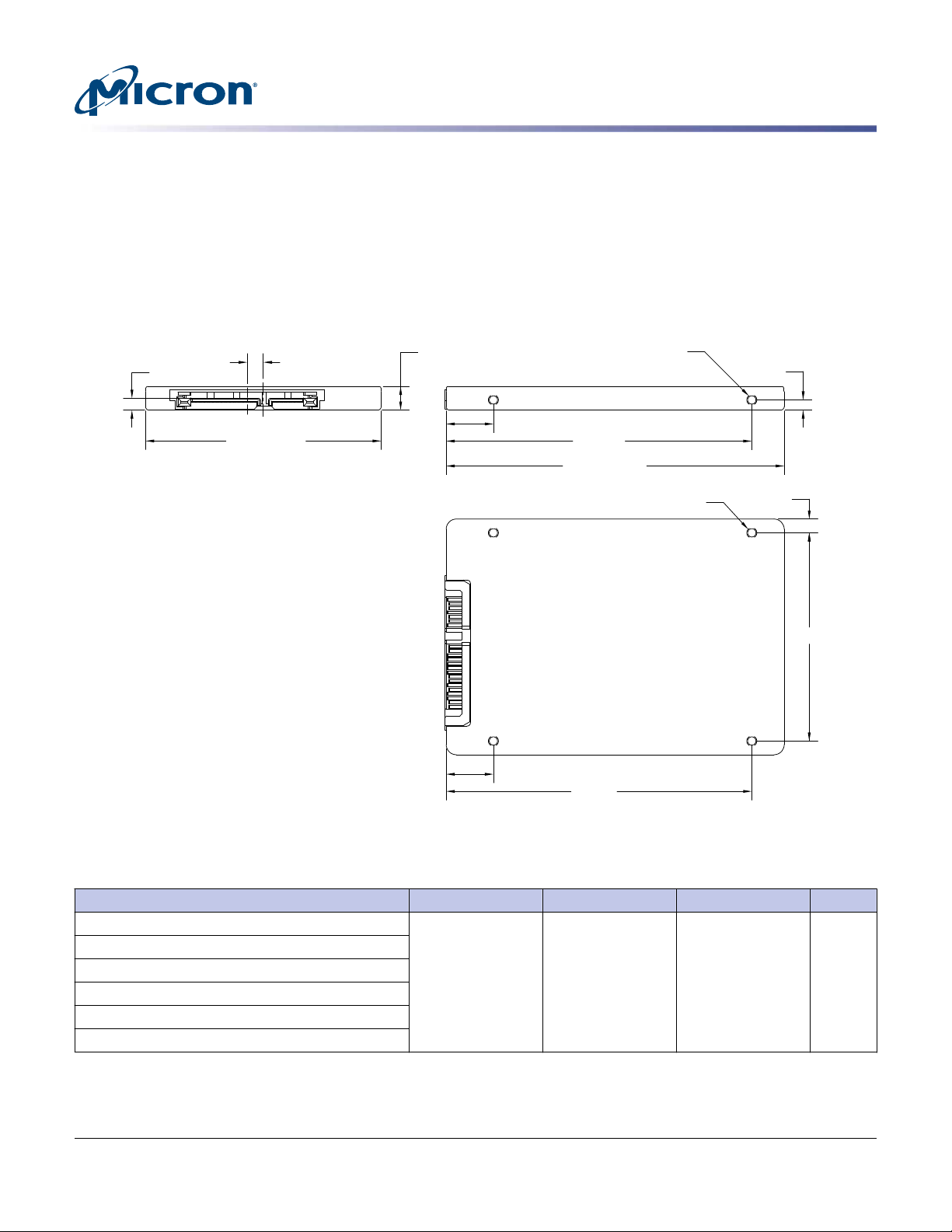
Physical Configuration
H +0.20/-0.50
L MAX
W ±0.25
(3.50)
(4.80)
(14.00)
(90.60)
(2X M3)
(Both sides)
(3.00)
(14.00)
(90.60)
(61.71)
(4.07)
(4X M3)
2.5-Inch 7mm
Product mass: less than 70 grams
Physical dimensions conform to the applicable form factor specifications as listed in
the figure below.
Figure 5: 2.5-Inch Package – 7mm
5100 Series NAND Flash SSD
Physical Configuration
Note:
Table 18: 2.5-Inch Package Dimensions
Capacity (GB) W L H Unit
240 69.85 100.45 7.00 mm
480
960
1920
3840
7680
Note:
CCMTD-1725822587-10309
5100_series_SSD_disti.pdf - Rev. A 12/16 EN
1. All dimensions are in millimeters.
1. Dimension values in millimeter per SFF 8201 Rev. 3.3.
29
Micron Technology, Inc. reserves the right to change products or specifications without notice.
© 2016 Micron Technology, Inc. All rights reserved.
Page 30

M.2 2280
Pin 1
Pin 75
L ±0.15
W ±0.15
B ±0.08
A MAX
C MAX
(3.50 DIA)
(5.50 DIA)
Product mass: less than 10 grams
Physical dimensions conform to the applicable form factor specifications as listed in
the figure below.
Figure 6: M.2 Type 2280 Package
5100 Series NAND Flash SSD
Physical Configuration
Note:
1. All dimensions are in millimeters.
Table 19: M.2 Type 2280 Package Dimensions
Capacity (GB) Specification W L A B C Unit
1920
CCMTD-1725822587-10309
5100_series_SSD_disti.pdf - Rev. A 12/16 EN
240 D5 22.00 80.00 1.50 0.80 1.50 mm
480
960
Note:
1. Dimension values in millimeter per PCI Express M.2 Specification Rev. 1.0.
30
Micron Technology, Inc. reserves the right to change products or specifications without notice.
© 2016 Micron Technology, Inc. All rights reserved.
Page 31

Compliance
5100 Series NAND Flash SSD
Compliance
Micron SSDs comply with the following:
• Micron Green Standard
• Built with sulfur resistant resistors
• CE (Europe): EN 55032 Class B, RoHS
• FCC: CFR Title 47, Part 15 Class B
• UL: UL-60950-1, 2nd Edition
• BSMI (Taiwan): approval to CNS 13438
• RCM (Australia, New Zealand): AS/NZS CISPR32 Class B
• KCC RRL (Korea): approval to KN 32 Class B, KN 35 Class B
• W.E.E.E.: Compliance with EU WEEE directive 2002/96/EC. Additional obligations
may apply to customers who place these products in the markets where WEEE is enforced
• TUV (Germany): approval to IEC60950/EN60950
• V
(Japan): 2015-04 Class B
CCI
• IC (Canada): CISPR32 Class B:
- This Class B digital apparatus complies with Canadian ICES-003:2016.
- Cet appareil numérique de la classe B est conforme à la norme NMB-003 du Canada.
FCC Rules
This equipment has been tested and found to comply with the limits for a Class B digital
device, pursuant to part 15 of the FCC Rules. These limits are designed to provide reasonable protection against harmful interference in a residential installation. This equipment generates, uses, and can radiate radio frequency energy and, if not installed and
used in accordance with the instructions, may cause harmful interference to radio communications. However, there is no guarantee that interference will not occur in a particular installation. If this equipment does cause harmful interference to radio or television reception, which can be determined by turning the equipment off and on, the user
is encouraged to try to correct the interference by one or more of the following measures:
• Reorient or relocate the receiving antenna.
• Increase the separation between the equipment and the receiver.
• Connect the equipment into an outlet on a circuit different from that to which the receiver is connected.
• Consult the dealer or an experienced radio/TV technician for help.
CCMTD-1725822587-10309
5100_series_SSD_disti.pdf - Rev. A 12/16 EN
31
Micron Technology, Inc. reserves the right to change products or specifications without notice.
© 2016 Micron Technology, Inc. All rights reserved.
Page 32

References
5100 Series NAND Flash SSD
References
• Serial ATA: High-speed serialized AT attachment, Serial ATA working group, available
at www.sata-io.org
• SATA 3.2 GOLD
• ATA-8 ACS-3 Revision 5
• SFF-8201 Rev. 3.3: For 2.5-Inch mechanical
• Trusted Computing Group (TCG) Enterprise Specification Version 1.00 Revision Final,
Revision 3.00 January 10, 2011. Available at www.trustedcomputinggroup.org
• PCI Express M.2 Specification rev 1.0: For M.2 mechanical.
CCMTD-1725822587-10309
5100_series_SSD_disti.pdf - Rev. A 12/16 EN
32
Micron Technology, Inc. reserves the right to change products or specifications without notice.
© 2016 Micron Technology, Inc. All rights reserved.
Page 33

Revision History
Rev. A – 12/16
5100 Series NAND Flash SSD
Revision History
• Initial release
8000 S. Federal Way, P.O. Box 6, Boise, ID 83707-0006, Tel: 208-368-4000
www.micron.com/products/support Sales inquiries: 800-932-4992
Micron and the Micron logo are trademarks of Micron Technology, Inc.
All other trademarks are the property of their respective owners.
This data sheet contains minimum and maximum limits specified over the power supply and temperature range set forth herein.
Although considered final, these specifications are subject to change, as further product development and data characterization some-
times occur.
CCMTD-1725822587-10309
5100_series_SSD_disti.pdf - Rev. A 12/16 EN
33
Micron Technology, Inc. reserves the right to change products or specifications without notice.
© 2016 Micron Technology, Inc. All rights reserved.
 Loading...