

Page 1

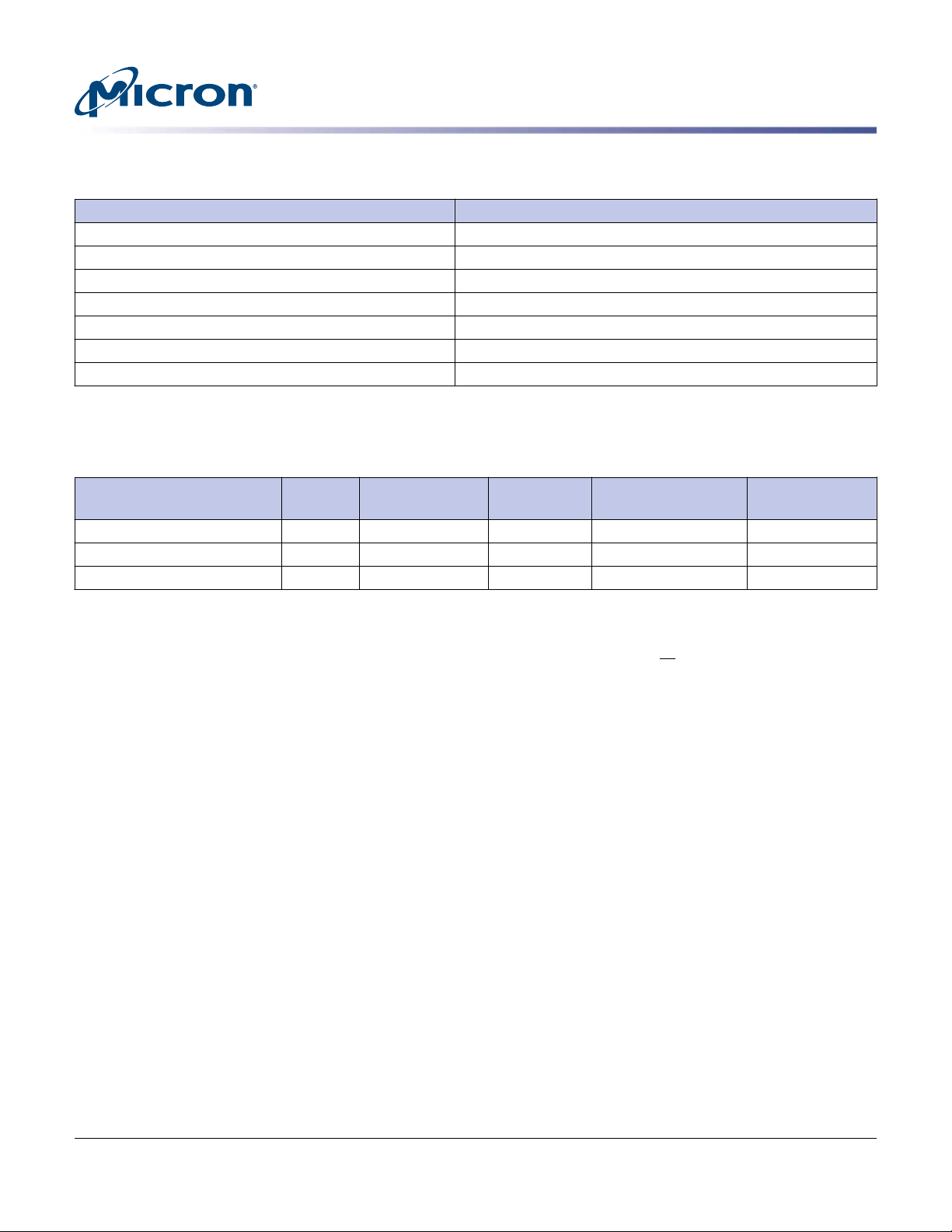
Module height: 31.25mm (1.23in)
64GB (x72, ECC, 3DS 2H Stack, 2 Package Ranks x 2 Logic
DDR4 3DS SDRAM RDIMM
MTA72ASS8G72PSZ – 64GB
Ranks) 288-Pin DDR4 RDIMM
Features
Features
• DDR4 functionality and operations supported as
defined in the component data sheet
• 288-pin, registered dual in-line memory module
(RDIMM)
• Fast data transfer rates: PC4-3200, PC4-2933, or
PC4-2666
• 64GB (8 Gig x 72)
• VDD = 1.20V (NOM)
• VPP = 2.5V (NOM)
• V
• Supports ECC error detection and correction
• Nominal and dynamic on-die termination (ODT) for
data, strobe, and mask signals
• Low-power auto self refresh (LPASR)
• On-die V
• Two package ranks x two logic ranks
• On-board I2C temperature sensor with integrated
serial presence-detect (SPD) EEPROM
• 16Gb, 3DS 2-high die stack x4 package, Master/Slave
control logic. Each die with16 internal banks; 4
groups of 4 banks each
• Fixed burst chop (BC) of 4 and burst length (BL) of 8
via the mode register set (MRS)
• Selectable BC4 or BL8 on-the-fly (OTF)
• Gold edge contacts
• Halogen-free
• Fly-by topology
• Terminated control, command, and address bus
= 2.5V (NOM)
DDSPD
generation and calibration
REFDQ
Figure 1: 288-Pin RDIMM (MO-309, R/C-B2)
Options Marking
• Operating temperature
– Commercial (0°C ≤ T
• Package
– 288-pin DIMM (halogen-free) Z
• Frequency/CAS latency
– 0.62ns @ CL = 26 (DDR4-3200) -3S2
– 0.682ns @ CL = 24 (DDR4-2933) -2S9
– 0.75ns @ CL = 22 (DDR4-2666) -2S6
≤ 95°C) None
OPER
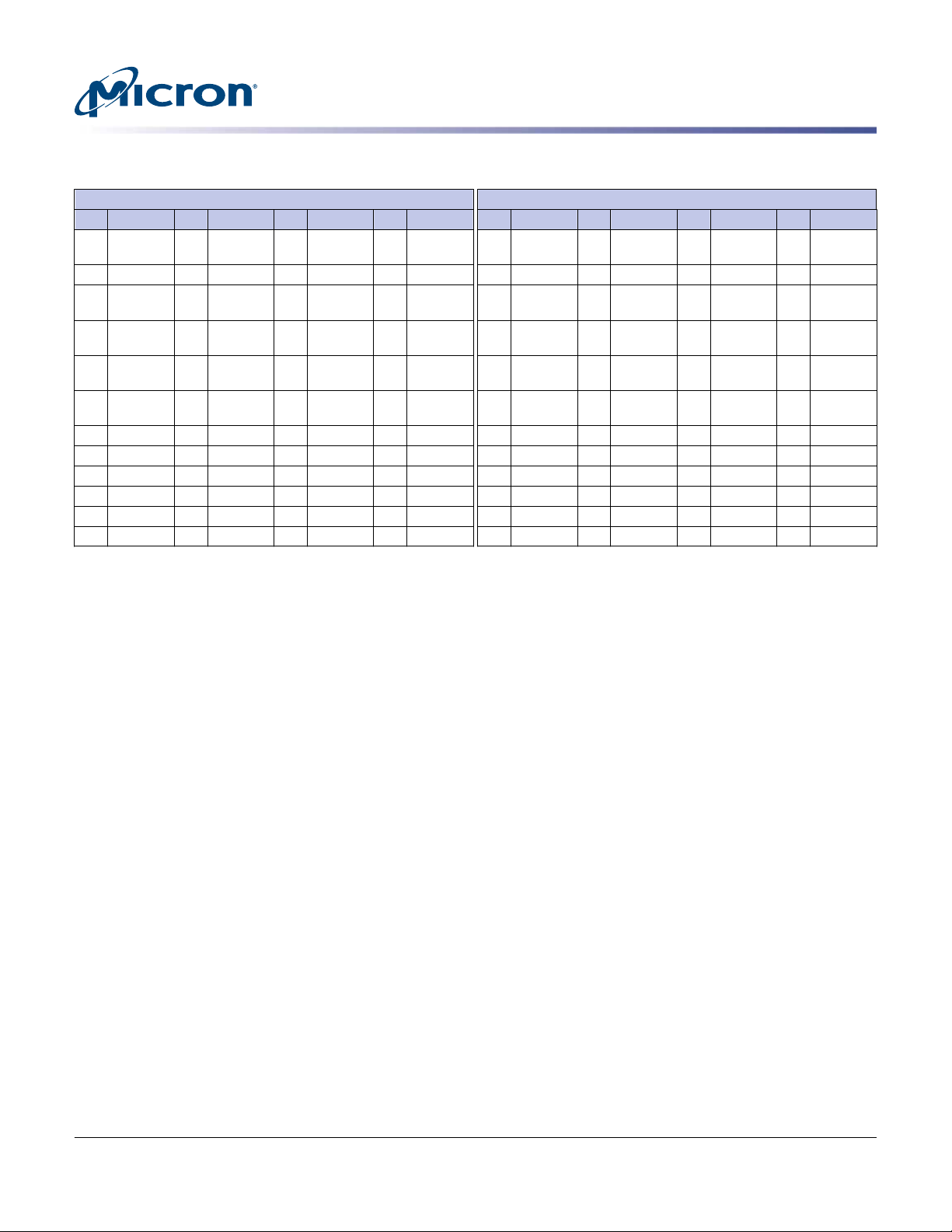
Table 1: Key Timing Parameters
Speed
Grade PC4-
-3S2 3200 3200 – – 2666 2666 2400 2400 2133 2133 1866 1600 13.75 13.75 45.75
-2S9 2933 – 2933 2933 2666 2666 2400 2400 2133 2133 1866 1600 14.32 14.32 46.32
-2S6 2666 – – – 2666 2666 2400 2400 2133 2133 1866 1600 14.25 14.25 46.25
-2S3 2400 – – – – – – 2400 – 2133 1866 1600 15 15 47
CCMTD-341111752-10423
ass72c8gx72psz.pdf - Rev. E 2/18 EN
Data Rate (MT/s)
CL =
t
28 –
26 25 24 24 22 22 20 20 18 16 14
1
Products and specifications discussed herein are subject to change by Micron without notice.
Micron Technology, Inc. reserves the right to change products or specifications without notice.
RCD
(ns)
© 2017 Micron Technology, Inc. All rights reserved.
t
RP
(ns)
t
RC
(ns)
Page 2
64GB (x72, ECC, 3DS 2H Stack, 2 Package Ranks x 2 Logic
Ranks) 288-Pin DDR4 RDIMM
Table 2: Addressing
Parameter 64GB
Row address 128K A[16:0]
Column address 1K A[9:0]
Device bank group address 4 BG[1:0]
Device bank address per group 4 BA[1:0]
Device configuration 16Gb (128 Meg x 4 x 16 banks x2 ranks)
Logic rank address 1 C0
Package rank address 2 CS_n[1:0]
Table 3: Part Numbers and Timing Parameters – 64GB Modules
Base device: MT40A4G4,1 16Gb DDR4 2H 3DS M/S DRAM DDR4 SDRAM
Part Number
2
Density Configuration
MTA72ASS8G72PSZ-3S2__ 64GB 8 Gig x 72 25.6 GB/s 0.62ns/3200 MT/s 26-22-22
MTA72ASS8G72PSZ-2S9__ 64GB 8 Gig x 72 23.47 GB/s 0.682ns/2933 MT/s 24-21-21
MTA72ASS8G72PSZ-2S6__ 64GB 8 Gig x 72 21.3 GB/s 0.75ns/2666 MT/s 22-19-19
Module
Module
Bandwidth
Memory Clock/
Data Rate
Clock Cycles
(CL-tRCD-tRP)
Features
Notes:
1. The data sheet for the base device can be found at micron.com.
2. All part numbers end with a two-place code (not shown) that designates component and PCB revisions.
Consult factory for current revision codes. Example: MTA72ASS8G72PSZ-3S2E1.
CCMTD-341111752-10423
ass72c8gx72psz.pdf - Rev. E 2/18 EN
2
Micron Technology, Inc. reserves the right to change products or specifications without notice.
© 2017 Micron Technology, Inc. All rights reserved.
Page 3

64GB (x72, ECC, 3DS 2H Stack, 2 Package Ranks x 2 Logic
Ranks) 288-Pin DDR4 RDIMM
Important Notes and Warnings
Important Notes and Warnings
Micron Technology, Inc. ("Micron") reserves the right to make changes to information published in this document,
including without limitation specifications and product descriptions. This document supersedes and replaces all
information supplied prior to the publication hereof. You may not rely on any information set forth in this document if you obtain the product described herein from any unauthorized distributor or other source not authorized
by Micron.
Automotive Applications. Products are not designed or intended for use in automotive applications unless specifically designated by Micron as automotive-grade by their respective data sheets. Distributor and customer/distributor shall assume the sole risk and liability for and shall indemnify and hold Micron harmless against all claims,
costs, damages, and expenses and reasonable attorneys' fees arising out of, directly or indirectly, any claim of
product liability, personal injury, death, or property damage resulting directly or indirectly from any use of nonautomotive-grade products in automotive applications. Customer/distributor shall ensure that the terms and conditions of sale between customer/distributor and any customer of distributor/customer (1) state that Micron
products are not designed or intended for use in automotive applications unless specifically designated by Micron
as automotive-grade by their respective data sheets and (2) require such customer of distributor/customer to indemnify and hold Micron harmless against all claims, costs, damages, and expenses and reasonable attorneys'
fees arising out of, directly or indirectly, any claim of product liability, personal injury, death, or property damage
resulting from any use of non-automotive-grade products in automotive applications.
Critical Applications. Products are not authorized for use in applications in which failure of the Micron component could result, directly or indirectly in death, personal injury, or severe property or environmental damage
("Critical Applications"). Customer must protect against death, personal injury, and severe property and environmental damage by incorporating safety design measures into customer's applications to ensure that failure of the
Micron component will not result in such harms. Should customer or distributor purchase, use, or sell any Micron
component for any critical application, customer and distributor shall indemnify and hold harmless Micron and
its subsidiaries, subcontractors, and affiliates and the directors, officers, and employees of each against all claims,
costs, damages, and expenses and reasonable attorneys' fees arising out of, directly or indirectly, any claim of
product liability, personal injury, or death arising in any way out of such critical application, whether or not Micron or its subsidiaries, subcontractors, or affiliates were negligent in the design, manufacture, or warning of the
Micron product.
Customer Responsibility. Customers are responsible for the design, manufacture, and operation of their systems,
applications, and products using Micron products. ALL SEMICONDUCTOR PRODUCTS HAVE INHERENT FAILURE RATES AND LIMITED USEFUL LIVES. IT IS THE CUSTOMER'S SOLE RESPONSIBILITY TO DETERMINE
WHETHER THE MICRON PRODUCT IS SUITABLE AND FIT FOR THE CUSTOMER'S SYSTEM, APPLICATION, OR
PRODUCT. Customers must ensure that adequate design, manufacturing, and operating safeguards are included
in customer's applications and products to eliminate the risk that personal injury, death, or severe property or environmental damages will result from failure of any semiconductor component.
Limited Warranty. In no event shall Micron be liable for any indirect, incidental, punitive, special or consequential
damages (including without limitation lost profits, lost savings, business interruption, costs related to the removal
or replacement of any products or rework charges) whether or not such damages are based on tort, warranty,
breach of contract or other legal theory, unless explicitly stated in a written agreement executed by Micron's duly
authorized representative.
CCMTD-341111752-10423
ass72c8gx72psz.pdf - Rev. E 2/18 EN
3
Micron Technology, Inc. reserves the right to change products or specifications without notice.
© 2017 Micron Technology, Inc. All rights reserved.
Page 4

64GB (x72, ECC, 3DS 2H Stack, 2 Package Ranks x 2 Logic
Ranks) 288-Pin DDR4 RDIMM
Pin Assignments
Pin Assignments
The pin assignment table below is a comprehensive list of all possible pin assignments
for DDR4 RDIMM modules. See the Functional Block Diagram for pins specific to this
module.
Table 4: Pin Assignments
288-Pin DDR4 RDIMM Front 288-Pin DDR4 RDIMM Back
Pin Symbol Pin Symbol Pin Symbol Pin Symbol Pin Symbol Pin Symbol Pin Symbol Pin Symbol
1 NC 37 V
2 V
38 DQ24 74 CK0_t 110 DQS14_t/
SS
3 DQ4 39 V
4 V
SS
40 DQS12_t/
TDQS12_t
5 DQ0 41 DQS12_c/
TDQS12_c
6 V
7 DQS9_t/
42 V
SS
43 DQ30 79 A0 115 DQ42 151 V
TDQS9_t
8 DQS09_c/
44 V
TDQS9_c
9 V
45 DQ26 81 BA0 117 DQ52 153 DQS0_t 189 V
SS
73 V
SS
75 CK0_c 111 DQS14_c/
SS
76 V
77 V
78 EVENT_n 114 V
SS
80 V
SS
DD
DD
TT
DD
109 V
145 NC 181 DQ29 217 V
SS
146 V
TDQS14_t
147 V
TDQS14_c
112 V
148 DQ5 184 V
SS
113 DQ46 149 V
150 DQ1 186 DQS3_t 222 PARITY 258 DQ47
SS
116 V
152 DQS0_c 188 DQ31 224 BA1 260 DQ43
SS
REFCA
SS
SS
SS
253 DQ41
DD
182 V
218 CK1_t 254 V
SS
183 DQ25 219 CK1_c 255 DQS5_c
220 V
SS
185 DQS3_c 221 V
187 V
223 V
SS
225 A10/AP261 V
SS
DD
TT
DD
256 DQS5_t
257 V
259 V
SS
SS
SS
SS
10 DQ6 46 V
11 V
47 CB4 83 V
SS
12 DQ2 48 V
13 V
49 CB0 85 V
SS
14 DQ12 50 V
15 V
SS
51 DQS17_t/
SS
SS
SS
TDQS17_t
16 DQ8 52 DQS17_c/
TDQS17_c
17 V
18 DQS10_t/
53 V
SS
54 CB6 90 V
SS
TDQS10_t
19 DQS10_c/
55 V
SS
TDQS10_c
20 V
21 DQ14 57 V
22 V
23 DQ10 59 V
24 V
56 CB2 92 V
SS
SS
58 RESET_n 94 V
SS
DD
60 CKE0 96 V
SS
82 RAS_n/
118 V
A16
119 DQ48 155 DQ7 191 V
DD
84 CS0_n 120 V
121 DQS15_t/
DD
TDQS15_t
86 CAS_n/
A15
122 DQS15_c/
TDQS15_c
87 ODT0 123 V
88 V
124 DQ54 160 V
DD
89 CS1_n/NC125 V
126 DQ50 162 V
DD
91 ODT1/NC127 V
128 DQ60 164 DQS1_t 200 V
DD
93 CS2_n/C0129 V
130 DQ56 166 DQ15 202 V
SS
95 DQ36 131 V
132 DQS16_t/
SS
TDQS16_t
SS
SS
154 V
156 V
190 DQ27 226 V
SS
SS
192 CB5 228 WE_n/
SS
DD
227 NC 263 V
A14
157 DQ3 193 V
158 V
159 DQ13 195 V
SS
161 DQ9 197 DQS8_t 233 V
SS
163 DQS1_c 199 CB7 235 NC/C2271 DQ51
SS
165 V
SS
194 CB1 230 NC 266 DQS6_c
SS
196 DQS8_c 232 A13 268 V
SS
198 V
SS
201 CB3 237 CS3_n/
SS
229 V
SS
231 V
SS
234 A17 270 V
SS
236 V
SS
DD
DD
DD
DD
C1, NC
238 SA2 274 V
SS
167 V
SS
168 DQ11 204 V
203 CKE1/NC239 V
SS
DD
SS
240 DQ37 276 V
262 DQ53
SS
264 DQ49
265 V
SS
267 DQS6_t
SS
269 DQ55
SS
272 V
SS
273 DQ61
SS
275 DQ57
SS
CCMTD-341111752-10423
ass72c8gx72psz.pdf - Rev. E 2/18 EN
4
Micron Technology, Inc. reserves the right to change products or specifications without notice.
© 2017 Micron Technology, Inc. All rights reserved.
Page 5
64GB (x72, ECC, 3DS 2H Stack, 2 Package Ranks x 2 Logic
Ranks) 288-Pin DDR4 RDIMM
Pin Assignments
Table 4: Pin Assignments (Continued)
288-Pin DDR4 RDIMM Front 288-Pin DDR4 RDIMM Back
Pin Symbol Pin Symbol Pin Symbol Pin Symbol Pin Symbol Pin Symbol Pin Symbol Pin Symbol
25 DQ20 61 V
26 V
62 ACT_n 98 V
SS
27 DQ16 63 BG0 99 DQS13_t/
28 V
29 DQS11_t/
64 V
SS
65 A12/BC_n 101 V
TDQS11_t
30 DQS11_c/
66 A9 102 DQ38 138 V
TDQS11_c
31 V
67 V
SS
32 DQ22 68 A8 104 DQ34 140 SA1 176 V
33 V
69 A6 105 V
SS
34 DQ18 70 V
35 V
71 A3 107 V
SS
36 DQ28 72 A1 108 DQ40 144 NC 180 V
97 DQ32 133 DQS16_c/
DD
SS
TDQ13_t
100 DQS13_c/
DD
TDQS13_c
SS
103 V
DD
106 DQ44 142 V
DD
SS
SS
SS
169 V
205 NC 241 V
SS
SS
277 DQS7_c
TDQS16_c
134 V
135 DQ62 171 V
136 V
137 DQ58 173 V
170 DQ21 206 V
SS
207 BG1 243 V
SS
172 DQ17 208 ALERT_n 244 DQS4_c 280 DQ63
SS
209 V
SS
174 DQS2_c 210 A11 246 V
SS
242 DQ33 278 DQS7_t
DD
SS
245 DQS4_t 281 V
DD
SS
279 V
282 DQ59
139 SA0 175 DQS2_t 211 A7 247 DQ39 283 V
SS
212 V
DD
248 V
284 V
SS
DDSPD
141 SCL 177 DQ23 213 A5 249 DQ35 285 SDA
143 V
178 V
PP
179 DQ19 215 V
PP
214 A4 250 V
SS
DD
216 A2 252 V
SS
286 V
SS
251 DQ45 287 V
288 V
SS
PP
PP
PP
SS
SS
SS
CCMTD-341111752-10423
ass72c8gx72psz.pdf - Rev. E 2/18 EN
5
Micron Technology, Inc. reserves the right to change products or specifications without notice.
© 2017 Micron Technology, Inc. All rights reserved.
Page 6
64GB (x72, ECC, 3DS 2H Stack, 2 Package Ranks x 2 Logic
Ranks) 288-Pin DDR4 RDIMM
Pin Descriptions
Pin Descriptions
The pin description table below is a comprehensive list of all possible pins for DDR4
modules. All pins listed may not be supported on this module. See Functional Block Diagram for pins specific to this module.
Table 5: Pin Descriptions
Symbol Type Description
Ax Input Address inputs: Provide the row address for ACTIVATE commands and the column address for
A10/AP Input Auto precharge: A10 is sampled during READ and WRITE commands to determine whether an
A12/BC_n Input Burst chop: A12/BC_n is sampled during READ and WRITE commands to determine if burst
ACT_n Input Command input: ACT_n defines the ACTIVATE command being entered along with CS_n. The
BAx Input Bank address inputs: Define the bank (with a bank group) to which an ACTIVATE, READ,
BGx Input Bank group address inputs: Define the bank group to which a REFRESH, ACTIVATE, READ,
C0, C1, C2
(RDIMM/LRDIMM on-
ly)
CKx_t
CKx_c
CKEx Input Clock enable: CKE HIGH activates and CKE LOW deactivates the internal clock signals, device
CSx_n Input Chip select: All commands are masked when CS_n is registered HIGH. CS_n provides external
Input Chip ID: These inputs are used only when devices are stacked; that is, 2H, 4H, and 8H stacks for
Input Clock: Differential clock inputs. All address, command, and control input signals are sampled
READ/WRITE commands in order to select one location out of the memory array in the respective bank (A10/AP, A12/BC_n, WE_n/A14, CAS_n/A15, and RAS_n/A16 have additional functions;
see individual entries in this table). The address inputs also provide the op-code during the
MODE REGISTER SET command. A17 is only defined for x4 SDRAM.
auto precharge should be performed on the accessed bank after a READ or WRITE operation
(HIGH = auto precharge; LOW = no auto precharge). A10 is sampled during a PRECHARGE command to determine whether the precharge applies to one bank (A10 LOW) or all banks (A10
HIGH). If only one bank is to be precharged, the bank is selected by the bank group and bank
addresses.
chop (on-the-fly) will be performed (HIGH = no burst chop; LOW = burst chopped). See Command Truth Table in the DDR4 component data sheet.
input into RAS_n/A16, CAS_n/A15, and WE_n/A14 are considered as row address A16, A15, and
A14. See Command Truth Table.
WRITE, or PRECHARGE command is being applied. Also determine which mode register is to be
accessed during a MODE REGISTER SET command.
WRITE, or PRECHARGE command is being applied. Also determine which mode register is to be
accessed during a MODE REGISTER SET command. BG[1:0] are used in the x4 and x8 configurations. x16-based SDRAM only has BG0.
x4 and x8 configurations using through-silicon vias (TSVs). These pins are not used in the x16
configuration. Some DDR4 modules support a traditional DDP package, which uses CS1_n,
CKE1, and ODT1 to control the second die. All other stack configurations, such as a 4H or 8H,
are assumed to be single-load (master/slave) type configurations where C0, C1, and C2 are used
as chip ID selects in conjunction with a single CS_n, CKE, and ODT. Chip ID is considered part of
the command code.
on the crossing of the positive edge of CK_t and the negative edge of CK_c.
input buffers, and output drivers. Taking CKE LOW provides PRECHARGE POWER-DOWN and
SELF REFRESH operations (all banks idle), or active power-down (row active in any bank). CKE is
asynchronous for self refresh exit. After V
tialization sequence, it must be maintained during all operations (including SELF REFRESH). CKE
must be maintained HIGH throughout read and write accesses. Input buffers (excluding CK_t,
CK_c, ODT, RESET_n, and CKE) are disabled during power-down. Input buffers (excluding CKE
and RESET_n) are disabled during self refresh.
rank selection on systems with multiple ranks. CS_n is considered part of the command code
(CS2_n and CS3_n are not used on UDIMMs).
has become stable during the power-on and ini-
REFCA
CCMTD-341111752-10423
ass72c8gx72psz.pdf - Rev. E 2/18 EN
6
Micron Technology, Inc. reserves the right to change products or specifications without notice.
© 2017 Micron Technology, Inc. All rights reserved.
Page 7
64GB (x72, ECC, 3DS 2H Stack, 2 Package Ranks x 2 Logic
Ranks) 288-Pin DDR4 RDIMM
Pin Descriptions
Table 5: Pin Descriptions (Continued)
Symbol Type Description
ODTx Input On-die termination: ODT (registered HIGH) enables termination resistance internal to the
PARITY Input Parity for command and address: This function can be enabled or disabled via the mode
RAS_n/A16
CAS_n/A15
WE_n/A14
RESET_n CMOS Input Active LOW asynchronous reset: Reset is active when RESET_n is LOW and inactive when RE-
SAx Input
SCL Input
DQx, CBx I/O Data input/output and check bit input/output: Bidirectional data bus. DQ represents
DM_n/DBI_n/
TDQS_t (DMU_n,
DBIU_n), (DML_n/
DBIl_n)
SDA I/O Serial Data: Bidirectional signal used to transfer data in or out of the EEPROM or EEPROM/TS
DQS_t
DQS_c
DQSU_t
DQSU_c
DQSL_t
DQSL_c
ALERT_n Output Alert output: Possesses functions such as CRC error flag and command and address parity error
EVENT_n Output Temperature event: The EVENT_n pin is asserted by the temperature sensor when critical tem-
Input Command inputs: RAS_n/A16, CAS_n/A15, and WE_n/A14 (along with CS_n) define the com-
I/O Input data mask and data bus inversion: DM_n is an input mask signal for write data. Input
I/O Data strobe: Output with read data, input with write data. Edge-aligned with read data, cen-
DDR4 SDRAM. When enabled, ODT (RTT) is applied only to each DQ, DQS_t, DQS_c, DM_n/
DBI_n/TDQS_t, and TDQS_c signal for x4 and x8 configurations (when the TDQS function is enabled via the mode register). For the x16 configuration, RTT is applied to each DQ, DQSU_t,
DQSU_c, DQSL_t, DQSL_c, UDM_n, and LDM_n signal. The ODT pin will be ignored if the mode
registers are programmed to disable RTT.
register. When enabled in MR5, the DRAM calculates parity with ACT_n, RAS_n/A16, CAS_n/A15,
WE_n/A14, BG[1:0], BA[1:0], A[16:0]. Input parity should be maintained at the rising edge of the
clock and at the same time as command and address with CS_n LOW.
mand and/or address being entered and have multiple functions. For example, for activation
with ACT_n LOW, these are addresses like A16, A15, and A14, but for a non-activation command with ACT_n HIGH, these are command pins for READ, WRITE, and other commands defined in Command Truth Table.
SET_n is HIGH. RESET_n must be HIGH during normal operation.
Serial address inputs: Used to configure the temperature sensor/SPD EEPROM address range
on the I2C bus.
Serial clock for temperature sensor/SPD EEPROM: Used to synchronize communication to
and from the temperature sensor/SPD EEPROM on the I2C bus.
DQ[3:0], DQ[7:0], and DQ[15:0] for the x4, x8, and x16 configurations, respectively. If cyclic redundancy checksum (CRC) is enabled via the mode register, the CRC code is added at the end of
the data burst. Any one or all of DQ0, DQ1, DQ2, or DQ3 may be used for monitoring of internal V
level during test via mode register setting MR[4] A[4] = HIGH; training times change
REF
when enabled.
data is masked when DM_n is sampled LOW coincident with that input data during a write access. DM_n is sampled on both edges of DQS. DM is multiplexed with the DBI function by the
mode register A10, A11, and A12 settings in MR5. For a x8 device, the function of DM or TDQS
is enabled by the mode register A11 setting in MR1. DBI_n is an input/output identifying
whether to store/output the true or inverted data. If DBI_n is LOW, the data will be stored/
output after inversion inside the DDR4 device and not inverted if DBI_n is HIGH. TDQS is only
supported in x8 SDRAM configurations (TDQS is not valid for UDIMMs).
combo device.
tered-aligned with write data. For x16 configurations, DQSL corresponds to the data on
DQ[7:0], and DQSU corresponds to the data on DQ[15:8]. For the x4 and x8 configurations, DQS
corresponds to the data on DQ[3:0] and DQ[7:0], respectively. DDR4 SDRAM supports a differential data strobe only and does not support a single-ended data strobe.
flag as output signal. If a CRC error occurs, ALERT_n goes LOW for the period time interval and
returns HIGH. If an error occurs during a command address parity check, ALERT_n goes LOW until the on-going DRAM internal recovery transaction is complete. During connectivity test mode,
this pin functions as an input. Use of this signal is system-dependent. If not connected as signal,
ALERT_n pin must be connected to VDD on DIMMs.
perature thresholds have been exceeded. This pin has no function (NF) on modules without
temperature sensors.
CCMTD-341111752-10423
ass72c8gx72psz.pdf - Rev. E 2/18 EN
7
Micron Technology, Inc. reserves the right to change products or specifications without notice.
© 2017 Micron Technology, Inc. All rights reserved.
Page 8
64GB (x72, ECC, 3DS 2H Stack, 2 Package Ranks x 2 Logic
Table 5: Pin Descriptions (Continued)
Symbol Type Description
TDQS_t
TDQS_c
(x8 DRAM-based
RDIMM only)
V
DD
V
PP
V
REFCA
V
SS
V
TT
V
DDSPD
RFU – Reserved for future use.
NC – No connect: No internal electrical connection is present.
NF – No function: May have internal connection present, but has no function.
Output Termination data strobe: When enabled via the mode register, the DRAM device enables the
same RTT termination resistance on TDQS_t and TDQS_c that is applied to DQS_t and DQS_c.
When the TDQS function is disabled via the mode register, the DM/TDQS_t pin provides the data mask (DM) function, and the TDQS_c pin is not used. The TDQS function must be disabled in
the mode register for both the x4 and x16 configurations. The DM function is supported only in
x8 and x16 configurations. DM, DBI, and TDQS are a shared pin and are enabled/disabled by
mode register settings. For more information about TDQS, see the DDR4 DRAM component data sheet (TDQS_t and TDQS_c are not valid for UDIMMs).
Supply Module power supply: 1.2V (TYP).
Supply DRAM activating power supply: 2.5V –0.125V / +0.250V.
Supply Reference voltage for control, command, and address pins.
Supply Ground.
Supply Power supply for termination of address, command, and control VDD/2.
Supply Power supply used to power the I2C bus for SPD.
Ranks) 288-Pin DDR4 RDIMM
Pin Descriptions
CCMTD-341111752-10423
ass72c8gx72psz.pdf - Rev. E 2/18 EN
8
Micron Technology, Inc. reserves the right to change products or specifications without notice.
© 2017 Micron Technology, Inc. All rights reserved.
Page 9

64GB (x72, ECC, 3DS 2H Stack, 2 Package Ranks x 2 Logic
DQ Map
Table 6: Component-to-Module DQ Map Front
Ranks) 288-Pin DDR4 RDIMM
DQ Map
Component
Reference
Number
U2 0 7 155 U3 0 15 166
U4 0 23 177 U5 0 31 188
U6 0 CB7 199 U8 0 39 247
U9 0 47 258 U10 0 55 269
U11 0 63 280 U12 0 3 157
U13 0 10 23 U14 0 16 27
U15 0 24 38 U16 0 CB0 49
U17 0 32 97 U18 0 41 253
Component
DQ Module DQ
1 5 148 1 13 159
2 6 10 2 14 21
3 4 3 3 12 14
1 21 170 1 29 181
2 22 32 2 30 43
3 20 25 3 28 36
1 CB5 192 1 37 240
2 CB6 54 2 38 102
3 CB4 47 3 36 95
1 45 251 1 53 262
2 46 113 2 54 124
3 44 106 3 52 117
1 61 273 1 1 150
2 62 135 2 2 12
3 60 128 3 0 5
1 9 161 1 18 34
2 11 168 2 17 172
3 8 16 3 19 179
1 26 45 1 CB2 56
2 25 183 2 CB1 194
3 27 190 3 CB3 201
1 34 104 1 42 115
2 33 242 2 40 108
3 35 249 3 43 260
Module Pin
Number
Component
Reference
Number
Component
DQ Module DQ
Module Pin
Number
CCMTD-341111752-10423
ass72c8gx72psz.pdf - Rev. E 2/18 EN
9
Micron Technology, Inc. reserves the right to change products or specifications without notice.
© 2017 Micron Technology, Inc. All rights reserved.
Page 10

64GB (x72, ECC, 3DS 2H Stack, 2 Package Ranks x 2 Logic
Table 6: Component-to-Module DQ Map Front (Continued)
Ranks) 288-Pin DDR4 RDIMM
DQ Map
Component
Reference
Number
Component
DQ Module DQ
Module Pin
Number
Component
Reference
Number
Component
DQ Module DQ
U19 0 51 271 U20 0 59 282
1 49 264 1 57 275
2 50 126 2 58 137
3 48 119 3 56 130
Table 7: Component-to-Module DQ Map Back
Component
Reference
Number
Component
DQ Module DQ
Module Pin
Number
U21 0 61 273 U22 0 53 262
1 63 280 1 55 269
2 60 128 2 52 117
3 62 135 3 54 124
U23 0 45 251 U24 0 37 240
1 47 258 1 39 247
2 44 106 2 36 95
3 46 113 3 38 102
U25 0 CB5 192 U26 0 29 181
1 CB7 199 1 31 188
2 CB4 47 2 28 36
3 CB6 54 3 30 43
U27 0 21 170 U28 0 13 159
1 23 177 1 15 166
2 20 25 2 12 14
3 22 32 3 14 21
U29 0 5 148 U30 0 57 275
1 7 155 1 59 282
2 4 3 2 56 130
3 6 10 3 58 137
U31 0 49 264 U32 0 42 115
1 51 271 1 41 253
2 48 119 2 43 260
3 50 126 3 40 108
Component
Reference
Number
Component
DQ Module DQ
Module Pin
Number
Module Pin
Number
CCMTD-341111752-10423
ass72c8gx72psz.pdf - Rev. E 2/18 EN
10
Micron Technology, Inc. reserves the right to change products or specifications without notice.
© 2017 Micron Technology, Inc. All rights reserved.
Page 11

64GB (x72, ECC, 3DS 2H Stack, 2 Package Ranks x 2 Logic
Table 7: Component-to-Module DQ Map Back (Continued)
Ranks) 288-Pin DDR4 RDIMM
DQ Map
Component
Reference
Number
Component
DQ Module DQ
Module Pin
Number
Component
Reference
Number
Component
DQ Module DQ
U33 0 34 104 U34 0 CB2 56
1 32 97 1 CB0 49
2 35 249 2 CB3 201
3 33 242 3 CB1 194
U35 0 26 45 U36 0 18 34
1 24 38 1 16 27
2 27 190 2 19 179
3 25 183 3 17 172
U37 0 9 161 U38 0 1 150
1 10 23 1 3 157
2 8 16 2 0 5
3 11 168 3 2 12
Module Pin
Number
CCMTD-341111752-10423
ass72c8gx72psz.pdf - Rev. E 2/18 EN
11
Micron Technology, Inc. reserves the right to change products or specifications without notice.
© 2017 Micron Technology, Inc. All rights reserved.
Page 12

Core
Memory
Array
Master
Control
Logic
CS#
CK, CK#
RAS#
WE#
CAS#
CKE
RESET#
C0
Command
Decode
Mode Registers
Mode Registers
A[15: 0]
BG[1:0]
BA[1:0]
Address
Registers
WRITE
Drivers
and input
Logic
DLL
READ
Drivers
ODT
ZQ CAL
ODT
ZQ
RZQ
V
SSQ
DM
DQ[n-0]
DQS, DQS#
Core
Memory
Array
Local
Control
Logic
Slave Die
Master Die
ODT
ODT Control
Local
Control
Logic
64GB (x72, ECC, 3DS 2H Stack, 2 Package Ranks x 2 Logic
3DS Device Functional Block Diagram
Figure 2: 2-high 3DS Device Functional Block Diagram
Ranks) 288-Pin DDR4 RDIMM
3DS Device Functional Block Diagram
CCMTD-341111752-10423
ass72c8gx72psz.pdf - Rev. E 2/18 EN
12
Micron Technology, Inc. reserves the right to change products or specifications without notice.
© 2017 Micron Technology, Inc. All rights reserved.
Page 13

A/BCS0_n
A/BCS1_n
A/BC0
U7
Rank 0: U2–U6, U8–U20
Rank 1: U21–38
A/BCS_n[1:0], A/BBA[1:0]A/BBG[1:0],
A/BACT_n, A/BA[17, 13:0], A/B-RAS_n/A16,
A/B-CAS_n/A15, A/B-WE_n/A14,
A/BCKE[1:0], A/BODT[1:0]
CK[3:0]_t
CK[3:0]_c
Command, control, address, and clock line terminations:
DDR4
SDRAM
VTT
DDR4
SDRAM
VDD
U1
A0
SPD EEPROM/
Temperature
sensor
A1 A2
SA0
SA1
SDA
SCL
EVT
EVENT#
CS0_n
CS1_n
BA[1:0]
BG[1:0]
ACT_n
A[17, 13:0]
RAS_n/A16
CAS_n/A15
WE_n/A14
CKE0
CKE1
ODT0
ODT1
PAR_IN
C[2:0]
ALERT_CONN
A/BCS0_n: Rank 0
A/BCS1_n: Rank 1
A/BBA[1:0]: DDR4 SDRAM
A/BBG[1:0]: DDR4 SDRAM
A/BACT_n: DDR4 SDRAM
A/BA[17,13:0]: DDR4 SDRAM
A/B-RAS_n/A16: DDR4 SDRAM
A/B-CAS_n/A15: DDR4 SDRAM
A/B-WE_n/A14: DDR4 SDRAM
A/BCKE0: Rank 0
A/BCKE1: Rank 1
A/BODT0: Rank 0
A/BODT1: Rank 1
A/BPAR: DDR4 SDRAM
C[2:0]: DDR4 SDRAM
ALERT_DRAM: DDR4 SDRAM
SA2
VREFCA
VSS
DDR4 SDRAM, Register
DDR4 SDRAM, Register
VDD
Control, command and
address termination
VDDSPD
SPD EEPROM/Temp Sensor,
Register
VTT
DDR4 SDRAM, Register
DDR4 SDRAM
VPP
R
E
G
I
S
T
E
R
&
P
L
L
RESET_CONN
CK[3:0]_c
DDR4 SDRAM
RESET_DRAM: DDR4 SDRAM
CK[3:0]_t
ZQ
VSS
SA0
SA1
SA2
SCL
SDA
M
DQ0
DQ1
DQ2
DQ3
U38
U12
S
CS_n DQS_t DQS_c C0
CS_n DQS_t DQS_c C0
DQS0_t
DQS0_c
V
SS
ZQ
V
SS
ZQ
DQ4
DQ5
DQ6
DQ7
U29
U2
CS_n DQS_t DQS_c C0
CS_n DQS_t DQS_c C0
DQS9_t
DQS9_c
V
SS
ZQ
V
SS
ZQ
DQ8
DQ9
DQ10
DQ11
U37
U13
CS_n DQS_t DQS_c C0
CS_n DQS_t DQS_c C0
DQS1_t
DQS1_c
V
SS
ZQ
V
SS
ZQ
DQ12
DQ13
DQ14
DQ15
U28
U3
CS_n DQS_t DQS_c C0
CS_n DQS_t DQS_c C0
DQS10_t
DQS10_c
V
SS
ZQ
V
SS
ZQ
U36
U14
CS_n DQS_t DQS_c C0
CS_n DQS_t DQS_c C0
DQS2_t
DQS2_c
V
SS
ZQ
V
SS
ZQ
DQ20
DQ21
DQ22
DQ23
U27
U4
CS_n DQS_t DQS_c C0
CS_n DQS_t DQS_c C0
DQS11_t
DQS11_c
V
SS
ZQ
V
SS
ZQ
DQ24
DQ25
DQ26
DQ27
U35
U15
CS_n DQS_t DQS_c C0
CS_n DQS_t DQS_c C0
DQS3_t
DQS3_c
V
SS
ZQ
V
SS
ZQ
DQ28
DQ29
DQ30
DQ31
U26
U5
CS_n DQS_t DQS_c C0
CS_n DQS_t DQS_c C0
DQS12_t
DQS12_c
V
SS
ZQ
V
SS
ZQ
CB0
CB1
CB2
CB3
U34
U16
CS_n DQS_t DQS_c C0
CS_n DQS_t DQS_c C0
DQS8_t
DQS8_c
V
SS
ZQ
V
SS
ZQ
CB4
CB5
CB6
CB7
U25U6
CS_n DQS_t DQS_c C0
CS_n DQS_t DQS_c C0
DQS17_t
DQS17_c
V
SS
ZQ
V
SS
ZQ
DQ32
DQ33
DQ34
DQ35
U33
U17
CS_n DQS_t DQS_c C0
CS_n DQS_t DQS_c C0
DQS4_t
DQS4_c
V
SS
ZQ
V
SS
ZQ
DQ36
DQ37
DQ38
DQ39
U24
U8
CS_n DQS_t DQS_c C0
CS_n DQS_t DQS_c C0
DQS13_t
DQS13_c
V
SS
ZQ
V
SS
ZQ
DQ40
DQ41
DQ42
DQ43
U32
U18
CS_n DQS_t DQS_c C0
CS_n DQS_t DQS_c C0
DQS5_t
DQS5_c
V
SS
ZQ
V
SS
ZQ
DQ44
DQ45
DQ46
DQ47
U23
U9
CS_n DQS_t DQS_c C0
CS_n DQS_t DQS_c C0
DQS14_t
DQS14_c
V
SS
ZQ
V
SS
ZQ
DQ48
DQ49
DQ50
DQ51
U31
U19
CS_n DQS_t DQS_c C0
CS_n DQS_t DQS_c C0
DQS6_t
DQS6_c
V
SS
ZQ
V
SS
ZQ
DQ52
DQ53
DQ54
DQ55
U22
U10
CS_n DQS_t DQS_c C0
CS_n DQS_t DQS_c C0
DQS15_t
DQS15_c
V
SS
ZQ
V
SS
ZQ
DQ56
DQ57
DQ58
DQ59
U30
U20
CS_n DQS_t DQS_c C0
CS_n DQS_t DQS_c C0
DQS7_t
DQS7_c
V
SS
ZQ
V
SS
ZQ
DQ60
DQ61
DQ62
DQ63
U21
U11
CS_n DQS_t DQS_c C0
CS_n DQS_t DQS_c C0
DQS16_t
DQS16_c
V
SS
ZQ
V
SS
ZQ
M
S
M
S
M
S
DQ16
DQ17
DQ18
DQ19
M
S
M
S
M
S
M
S
M
S
M
S
M
S
M
S
M
S
M
S
M
S
M
S
M
S
M
S
M
S
M
S
M
S
M
S
M
S
M
S
M
S
M
S
M
S
M
S
M
S
M
S
M
S
M
S
M
S
M
S
M
S
M
S
CK0_t
CK0_c
CK1_t
CK1_c
64GB (x72, ECC, 3DS 2H Stack, 2 Package Ranks x 2 Logic
Module Functional Block Diagram
Figure 3: Functional Block Diagram, R/C-B2
CCMTD-341111752-10423
ass72c8gx72psz.pdf - Rev. E 2/18 EN
Note:
1. The ZQ ball on each DDR4 component is connected to an external 240Ω ±1% resistor
that is tied to ground. It is used for the calibration of the component’s ODT and output
driver.
13
Ranks) 288-Pin DDR4 RDIMM
Module Functional Block Diagram
Micron Technology, Inc. reserves the right to change products or specifications without notice.
© 2017 Micron Technology, Inc. All rights reserved.
Page 14

General Description
High-speed DDR4 SDRAM modules use DDR4 SDRAM devices with two or four internal
memory bank groups. DDR4 SDRAM modules utilizing 4- and 8-bit-wide DDR4 SDRAM
devices have four internal bank groups consisting of four memory banks each, providing a total of 16 banks. 16-bit-wide DDR4 SDRAM devices have two internal bank
groups consisting of four memory banks each, providing a total of eight banks. DDR4
SDRAM modules benefit from DDR4 SDRAM's use of an 8n-prefetch architecture with
an interface designed to transfer two data words per clock cycle at the I/O pins. A single
READ or WRITE operation for the DDR4 SDRAM effectively consists of a single 8n-bitwide, four-clock data transfer at the internal DRAM core and eight corresponding n-bitwide, one-half-clock-cycle data transfers at the I/O pins.
DDR4 modules use two sets of differential signals: DQS_t and DQS_c to capture data
and CK_t and CK_c to capture commands, addresses, and control signals. Differential
clocks and data strobes ensure exceptional noise immunity for these signals and provide precise crossing points to capture input signals.
Fly-By Topology
DDR4 modules use faster clock speeds than earlier DDR technologies, making signal
quality more important than ever. For improved signal quality, the clock, control, command, and address buses have been routed in a fly-by topology, where each clock, control, command, and address pin on each DRAM is connected to a single trace and terminated (rather than a tree structure, where the termination is off the module near the
connector). Inherent to fly-by topology, the timing skew between the clock and DQS signals can be easily accounted for by using the write-leveling feature of DDR4.
64GB (x72, ECC, 3DS 2H Stack, 2 Package Ranks x 2 Logic
Ranks) 288-Pin DDR4 RDIMM
General Description
Module Manufacturing Location
Micron Technology manufactures modules at sites world-wide. Customers may receive
modules from any of the following manufacturing locations:
Table 8: DRAM Module Manufacturing Locations
Manufacturing Site Location Country of Origin Specified on Label
Boise, USA USA
Aguadilla, Puerto Rico Puerto Rico
Xian, China China
Singapore Singapore
CCMTD-341111752-10423
ass72c8gx72psz.pdf - Rev. E 2/18 EN
14
Micron Technology, Inc. reserves the right to change products or specifications without notice.
© 2017 Micron Technology, Inc. All rights reserved.
Page 15

64GB (x72, ECC, 3DS 2H Stack, 2 Package Ranks x 2 Logic
Address Mapping to DRAM
Address Mirroring
To achieve optimum routing of the address bus on DDR4 multi rank modules, the address bus will be wired as shown in the table below, or mirrored. For quad rank modules, ranks 1 and 3 are mirrored and ranks 0 and 2 are non-mirrored. Highlighted address pins have no secondary functions allowing for normal operation when crosswired. Data is still read from the same address it was written. However, Load Mode operations require a specific address. This requires the controller to accommodate for a
rank that is "mirrored." Systems may reference DDR4 SPD to determine if the module
has mirroring implemented or not. See the JEDEC DDR4 SPD specification for more details.
Table 9: Address Mirroring
Edge Connector Pin DRAM Pin, Non-mirrored DRAM Pin, Mirrored
A0 A0 A0
A1 A1 A1
A2 A2 A2
A3 A3 A4
A4 A4 A3
A5 A5 A6
A6 A6 A5
A7 A7 A8
A8 A8 A7
A9 A9 A9
A10 A10 A10
A11 A11 A13
A13 A13 A11
A12 A12 A12
A14 A14 A14
A15 A15 A15
A16 A16 A16
A17 A17 A17
BA0 BA0 BA1
BA1 BA1 BA0
BG0 BG0 BG1
BG1 BG1 BG0
Ranks) 288-Pin DDR4 RDIMM
Address Mapping to DRAM
CCMTD-341111752-10423
ass72c8gx72psz.pdf - Rev. E 2/18 EN
15
Micron Technology, Inc. reserves the right to change products or specifications without notice.
© 2017 Micron Technology, Inc. All rights reserved.
Page 16

64GB (x72, ECC, 3DS 2H Stack, 2 Package Ranks x 2 Logic
Registering Clock Driver Operation
Registered DDR4 SDRAM modules use a registering clock driver device consisting of a
register and a phase-lock loop (PLL). The device complies with the JEDEC DDR4 RCD
specification.
To reduce the electrical load on the host memory controller's command, address, and
control bus, Micron's RDIMMs utilize a DDR4 registering clock driver (RCD). The RCD
presents a single load to the controller while redriving signals to the DDR4 SDRAM devices, which helps enable higher densities and increase signal integrity. The RCD also
provides a low-jitter, low-skew PLL that redistributes a differential clock pair to multiple
differential pairs of clock outputs.
Control Words
The RCD device(s) used on DDR4 RDIMMs, LRDIMMs, and NVDIMMs contain configuration registers known as control words, which the host uses to configure the RCD
based on criteria determined by the module design. Control words can be set by the
host controller through either the DRAM address and control bus or the I2C bus interface. The RCD I2C bus interface resides on the same I2C bus interface as the module
temperature sensor and EEPROM.
Ranks) 288-Pin DDR4 RDIMM
Registering Clock Driver Operation
Parity Operations
Rank Addressing
The RCD includes a parity-checking function that can be enabled or disabled in control
word RC0E. The RCD receives a parity bit at the DPAR input from the memory controller and compares it with the data received on the qualified command and address inputs; it indicates on its open-drain ALERT_n pin whether a parity error has occurred. If
parity checking is enabled, the RCD forwards commands to the SDRAM when no parity
error has occurred. If the parity error function is disabled, the RCD forwards sampled
commands to the SDRAM regardless of whether a parity error has occurred. Parity is also checked during control word WRITE operations unless parity checking is disabled.
The chip select pins (CS_n) on Micron's modules are used to select a specific rank of
DRAM. The RDIMM is capable of selecting ranks in one of three different operating
modes, dependant on setting DA[1:0] bits in the DIMM configuration control word located within the RCD. Direct DualCS mode is utilized for single- or dual-rank modules.
For quad-rank modules, either direct or encoded QuadCS mode is used.
CCMTD-341111752-10423
ass72c8gx72psz.pdf - Rev. E 2/18 EN
16
Micron Technology, Inc. reserves the right to change products or specifications without notice.
© 2017 Micron Technology, Inc. All rights reserved.
Page 17

64GB (x72, ECC, 3DS 2H Stack, 2 Package Ranks x 2 Logic
Ranks) 288-Pin DDR4 RDIMM
Temperature Sensor with SPD EEPROM Operation
Temperature Sensor with SPD EEPROM Operation
Thermal Sensor Operations
The integrated thermal sensor continuously monitors the temperature of the module
PCB directly below the device and updates the temperature data register. Temperature
data may be read from the bus host at any time, which provides the host real-time feedback of the module's temperature. Multiple programmable and read-only temperature
registers can be used to create a custom temperature-sensing solution based on system
requirements and JEDEC JC-42.2.
EVENT_n Pin
The temperature sensor also adds the EVENT_n pin (open-drain), which requires a pullup to V
can be set up in the sensor’s configuration registers. EVENT_n is not used by the serial
presence-detect (SPD) EEPROM.
EVENT_n has three defined modes of operation: interrupt, comparator, and TCRIT. In
interrupt mode, the EVENT_n pin remains asserted until it is released by writing a 1 to
the clear event bit in the status register. In comparator mode, the EVENT_n pin clears
itself when the error condition is removed. Comparator mode is always used when the
temperature is compared against the TCRIT limit. In TCRIT only mode, the EVENT_n
pin is only asserted if the measured temperature exceeds the TCRIT limit; it then remains asserted until the temperature drops below the TCRIT limit minus the TCRIT
hysteresis.
. EVENT_n is a temperature sensor output used to flag critical events that
DDSPD
SPD EEPROM Operation
DDR4 SDRAM modules incorporate SPD. The SPD data is stored in a 512-byte, JEDEC
JC-42.4-compliant EEPROM that is segregated into four 128-byte, write-protectable
blocks. The SPD content is aligned with these blocks as shown in the table below.
Block Range Description
0 0–127 000h–07Fh Configuration and DRAM parameters
1 128–255 080h–0FFh Module parameters
2 256–319 100h–13Fh Reserved (all bytes coded as 00h)
320–383 140h–17Fh Manufacturing information
3 384–511 180h–1FFh End-user programmable
The first 384 bytes are programmed by Micron to comply with JEDEC standard JC-45,
"Appendix X: Serial Presence Detect (SPD) for DDR4 SDRAM Modules." The remaining
128 bytes of storage are available for use by the customer.
The EEPROM resides on a two-wire I2C serial interface and is not integrated with the
memory bus in any manner. It operates as a slave device in the I2C bus protocol, with all
operations synchronized by the serial clock. Transfer rates of up to 1 MHz are achievable at 2.5V (NOM).
Micron implements reversible software write protection on DDR4 SDRAM-based modules. This prevents the lower 384 bytes (bytes 0 to 383) from being inadvertently programmed or corrupted. The upper 128 bytes remain available for customer use and are
unprotected.
CCMTD-341111752-10423
ass72c8gx72psz.pdf - Rev. E 2/18 EN
17
Micron Technology, Inc. reserves the right to change products or specifications without notice.
© 2017 Micron Technology, Inc. All rights reserved.
Page 18

64GB (x72, ECC, 3DS 2H Stack, 2 Package Ranks x 2 Logic
Ranks) 288-Pin DDR4 RDIMM
Electrical Specifications
Electrical Specifications
Stresses greater than those listed may cause permanent damage to the module. This is a
stress rating only, and functional operation of the module at these or any other conditions outside those indicated in each device's data sheet is not implied. Exposure to absolute maximum rating conditions for extended periods may adversely affect reliability.
Table 10: Absolute Maximum Ratings
Symbol Parameter Min Max Units Notes
V
V
DDQ
V
VIN, V
Table 11: Operating Conditions
Symbol Parameter Min Nom Max Units Notes
V
V
V
REFCA(DC)
I
VTT
V
I
I
ZQ
I
I/O
I
OZpd
I
OZpu
I
VREFCAVREFCA
VDD supply voltage relative to V
DD
V
supply voltage relative to V
DDQ
Voltage on VPP pin relative to V
PP
Voltage on any pin relative to V
OUT
DD
VDD supply voltage 1.14 1.20 1.26 V 1
DRAM activating power supply 2.375 2.5 2.75 V 2
PP
Input reference voltage –
command/address bus
Termination reference current from V
Termination reference voltage (DC) –
TT
command/address bus
IN
Input leakage current; any input excluding ZQ; 0V <
VIN < 1.1V
Input leakage current; ZQ –3 – 3 µA 6, 7
DQ leakage; 0V < VIN < V
Output leakage current; V
Output leakage current; V
are disabled; ODT is disabled with ODT input HIGH
leakage; V
tialized)
SS
SS
SS
SS
DD
= VDD; DQ is disabled – – 5 µA
OUT
= VSS; DQ and ODT
OUT
= VDD/2 (after DRAM is ini-
REFCA
–0.4 1.5 V 1
–0.4 1.5 V 1
–0.4 3.0 V 2
–0.4 1.5 V
0.49 × V
TT
–750 – 750 mA
0.49 × VDD 20mV
0.5 × V
DD
DD
0.5 × VDD0.51 × VDD +
0.51 × V
20mV
DD
V 3
V 4
–2 – 2 µA 5
–4 – 4 µA 7
– – 50 µA
–2 – 2 µA 7
CCMTD-341111752-10423
ass72c8gx72psz.pdf - Rev. E 2/18 EN
Notes:
1. V
balls on DRAM are tied to VDD.
DDQ
2. VPP must be greater than or equal to VDD at all times.
3. V
must not be greater than 0.6 × VDD. When VDD is less than 500mV, V
REFCA
may be
REF
less than or equal to 300mV.
4. VTT termination voltages in excess of specification limit adversely affect command and
address signals' voltage margins and reduce timing margins.
5. Command and address inputs are terminated to VDD/2 in the registering clock driver. Input current is dependent on termination resistance set in the registering clock driver.
6. Tied to ground. Not connected to edge connector.
7. Multiply by number of DRAM die on module.
18
Micron Technology, Inc. reserves the right to change products or specifications without notice.
© 2017 Micron Technology, Inc. All rights reserved.
Page 19

64GB (x72, ECC, 3DS 2H Stack, 2 Package Ranks x 2 Logic
Ranks) 288-Pin DDR4 RDIMM
Electrical Specifications
Table 12: Thermal Characteristics
Symbol Parameter/Condition Value Units Notes
T
C
T
C
T
OPER
T
OPER
T
STG
RH
STG
NA Change rate of storage temperature 20 °C/hour
Commercial operating case temperature 0 to 85 °C 1, 2, 3
>85 to 95 °C 1, 2, 3, 4
Normal operating temperature range 0 to 85 °C 5, 7
Extended temperature operating range (optional) >85 to 95 °C 5, 7
Non-operating storage temperature –55 to 100 °C 6
Non-operating storage relative humidity (non-condensing) 5 to 95 %
Notes:
1. Maximum operating case temperature; TC is measured in the center of the package.
2. A thermal solution must be designed to ensure the DRAM device does not exceed the
maximum TC during operation.
3. Device functionality is not guaranteed if the DRAM device exceeds the maximum TC during operation.
4. If TC exceeds 85°C, the DRAM must be refreshed externally at 2X refresh, which is a 3.9µs
interval refresh rate.
5. The refresh rate must double when 85°C < T
OPER
≤ 95°C.
6. Storage temperature is defined as the temperature of the top/center of the DRAM and
does not reflect the storage temperatures of shipping trays.
7. For additional information, refer to technical note TN-00-08: "Thermal Applications"
available at micron.com.
CCMTD-341111752-10423
ass72c8gx72psz.pdf - Rev. E 2/18 EN
19
Micron Technology, Inc. reserves the right to change products or specifications without notice.
© 2017 Micron Technology, Inc. All rights reserved.
Page 20

64GB (x72, ECC, 3DS 2H Stack, 2 Package Ranks x 2 Logic
Ranks) 288-Pin DDR4 RDIMM
DRAM Operating Conditions
DRAM Operating Conditions
Recommended AC operating conditions are given in the DDR4 component data sheets.
Component specifications are available at micron.com. Module speed grades correlate
with component speed grades, as shown below.
Table 13: Module and Component Speed Grades
DDR4 components may exceed the listed module speed grades; module may not be available in all listed speed grades
Module Speed Grade Component Speed Grade
-3S2 -062H
-2S9 -068H
-2S6 -075H
-2S3 -083H
-2S1 -093H
Design Considerations
Simulations
Micron memory modules are designed to optimize signal integrity through carefully designed terminations, controlled board impedances, routing topologies, trace length
matching, and decoupling. However, good signal integrity starts at the system level. Micron encourages designers to simulate the signal characteristics of the system's memory bus to ensure adequate signal integrity of the entire memory system.
Power
Operating voltages are specified at the edge connector of the module, not at the DRAM.
Designers must account for any system voltage drops at anticipated power levels to ensure the required supply voltage is maintained.
CCMTD-341111752-10423
ass72c8gx72psz.pdf - Rev. E 2/18 EN
20
Micron Technology, Inc. reserves the right to change products or specifications without notice.
© 2017 Micron Technology, Inc. All rights reserved.
Page 21

64GB (x72, ECC, 3DS 2H Stack, 2 Package Ranks x 2 Logic
Ranks) 288-Pin DDR4 RDIMM
IDD Specifications
IDD Specifications
Table 14: DDR4 IDD Specifications and Conditions – 64GB (Die Revision G)
Values are for the MT40A4G4 DDR4 2H 3DS SDRAM only and are computed from values specified in the DDR4 3DS (16 Gig
x 4) component data sheet
Parameter Symbol 2666 Units
One bank ACTIVATE-PRECHARGE current I
One bank ACTIVATE-PRECHARGE, wordline boost, IPP current I
One bank ACTIVATE-READ-PRECHARGE current I
Precharge standby current I
Precharge standby ODT current I
Precharge power-down current I
Precharge quite standby current I
Active standby current I
Active standby IPP current I
Active power-down current I
Burst read current I
Burst write current I
Burst refresh current (1x REF) I
Burst refresh IPP current (1x REF) I
Self refresh current: Normal temperature range (0°C to 85°C) I
Self refresh current: Extended temperature range (0°C to 95°C) I
Self refresh current: Reduced temperature range (0°C to 45°C) I
Auto self refresh current (25°C) I
Auto self refresh current (45°C) I
Auto self refresh current (75°C) I
Auto self refresh IPP current I
Bank interleave read current I
Bank interleave read IPP current I
Maximum power-down current I
CDD0
CPP0
CDD1
CDD2N
CDD2NT
CDD2P
CDD2Q
CDD3N
CPP3N
CDD3P
CDD4R
CDD4W
CDD5R
CPP5R
CDD6N
CDD6E
CDD6R
CDD6A
CDD6A
CDD6A
CPP6X
CDD7
CPP7
CDD8
2232 mA
216 mA
2448 mA
1980 mA
2250 mA
1800 mA
1890 mA
2178 mA
216 mA
1962 mA
3582 mA
3510 mA
2448 mA
252 mA
2016 mA
2196 mA
1656 mA
1209.6 mA
1656 mA
2016 mA
288 mA
5004 mA
486 mA
1800 mA
CCMTD-341111752-10423
ass72c8gx72psz.pdf - Rev. E 2/18 EN
21
Micron Technology, Inc. reserves the right to change products or specifications without notice.
© 2017 Micron Technology, Inc. All rights reserved.
Page 22

64GB (x72, ECC, 3DS 2H Stack, 2 Package Ranks x 2 Logic
Ranks) 288-Pin DDR4 RDIMM
IDD Specifications
Table 15: DDR4 IDD Specifications and Conditions – 64GB (Die Revision E)
Values are for the MT40A4G4 DDR4 2H 3DS SDRAM only and are computed from values specified in the DDR4 3DS (16 Gig
x 4) component data sheet
Parameter Symbol 3200 2933 2666 Units
One bank ACTIVATE-PRECHARGE current I
One bank ACTIVATE-PRECHARGE, wordline boost, IPP current I
One bank ACTIVATE-READ-PRECHARGE current I
Precharge standby current I
Precharge standby ODT current I
Precharge power-down current I
Precharge quite standby current I
Active standby current I
Active standby IPP current I
Active power-down current I
Burst read current I
Burst write current I
Burst refresh current (1x REF) I
Burst refresh IPP current (1x REF) I
Self refresh current: Normal temperature range (0°C to 85°C) I
Self refresh current: Extended temperature range (0°C to 95°C) I
Self refresh current: Reduced temperature range (0°C to 45°C) I
Auto self refresh current (25°C) I
Auto self refresh current (45°C) I
Auto self refresh current (75°C) I
Auto self refresh IPP current I
Bank interleave read current I
Bank interleave read IPP current I
Maximum power-down current I
CDD0
CPP0
CDD1
CDD2N
CDD2NT
CDD2P
CDD2Q
CDD3N
CPP3N
CDD3P
CDD4R
CDD4W
CDD5R
CPP5R
CDD6N
CDD6E
CDD6R
CDD6A
CDD6A
CDD6A
CPP6X
CDD7
CPP7
CDD8
2340 2286 2232 mA
216 216 216 mA
2256 2502 2448 mA
2016 1998 1980 mA
2430 2340 2250 mA
1800 1800 1800 mA
1890 1890 1890 mA
2286 2232 2178 mA
216 216 216 mA
2034 1998 1962 mA
4158 3960 3762 mA
3834 3672 3510 mA
2538 2502 2448 mA
252 252 252 mA
2124 2124 2124 mA
2556 2556 2556 mA
1656 1656 1656 mA
1209.6 1209.6 1209.6 mA
1656 1656 1656 mA
2016 2016 2016 mA
288 288 288 mA
5544 5274 5004 mA
522 504 486 mA
1800 1800 1800 mA
CCMTD-341111752-10423
ass72c8gx72psz.pdf - Rev. E 2/18 EN
22
Micron Technology, Inc. reserves the right to change products or specifications without notice.
© 2017 Micron Technology, Inc. All rights reserved.
Page 23

64GB (x72, ECC, 3DS 2H Stack, 2 Package Ranks x 2 Logic
Ranks) 288-Pin DDR4 RDIMM
Registering Clock Driver Specifications
Registering Clock Driver Specifications
Table 16: Registering Clock Driver Electrical Characteristics
DDR4 RCD01 devices or equivalent
Parameter Symbol Pins Min Nom Max Units
DC supply voltage V
DC reference voltage V
DC termination
voltage
High-level input
V
IH. CMOS
voltage
Low-level input
V
IL. CMOS
voltage
DRST_n pulse width
IT_Pow-
er_stable
AC high-level output
V
voltage
AC low-level output
V
voltage
AC differential out-
V
OHdiff(AC)
put high measurement level (for output slew rate)
AC differential out-
V
OLdiff(AC)
put low measurement level (for output slew rate)
DD
REF
V
TT
t
IN-
OH(AC)
OL(AC)
All outputs except
Yn_t - Yn_c, BCK_t -
– 1.14 1.2 1.26 V
V
REFCA
– V
DRST_n 0.65 × V
0.49 × V
REF
DD
- 40mV V
DD
0.5 × V
DD
REF
– V
0 – 0.35 × V
0.51 × V
V
REF
DD
+ 40mV V
DD
DD
– 1.0 – – µs
VTT + (0.15 × VDD) – – V
ALERT_n
– – VTT + (0.15 × VDD) V
– 0.3 × V
DD
– mV
BCK_c
– –0.3 × V
DD
– mV
V
V
V
CCMTD-341111752-10423
ass72c8gx72psz.pdf - Rev. E 2/18 EN
Note:
1. Timing and switching specifications for the register listed are critical for proper operation of DDR4 SDRAM RDIMMs. These are meant to be a subset of the parameters for the
specific device used on the module. See the JEDEC RCD01 specification for complete operating electrical characteristics. Registering clock driver parametric values are specified
for device default control word settings, unless otherwise stated. The RC0A control
word setting does not affect parametric values.
23
Micron Technology, Inc. reserves the right to change products or specifications without notice.
© 2017 Micron Technology, Inc. All rights reserved.
Page 24

64GB (x72, ECC, 3DS 2H Stack, 2 Package Ranks x 2 Logic
Ranks) 288-Pin DDR4 RDIMM
Temperature Sensor with SPD EEPROM
Temperature Sensor with SPD EEPROM
The temperature sensor continuously monitors the module's temperature and can be
read back at any time over the I2C bus shared with the serial presence-detect (SPD) EEPROM. Refer to JEDEC JC-42.4 EE1004 and TSE2004 device specifications for complete
details.
SPD Data
For the latest SPD data, refer to Micron's SPD page: micron.com/SPD.
Table 17: Temperature Sensor with SPD EEPROM Operating Conditions
Parameter/Condition Symbol Min Nom Max Units
Supply voltage V
DDSPD
Input low voltage: logic 0; all inputs V
Input high voltage: logic 1; all inputs V
Output low voltage: 3mA sink current V
Input leakage current: (SCL, SDA) VIN = V
Output leakage current: V
OUT
= V
DDSPD
> 2V V
DDSPD
or V
DDSPD
or V
SSSPD
SSSPD
, SDA in High-Z I
IL
IH
OL
I
LI
LO
– 2.5 – V
–0.5 – V
V
× 0.7 – V
DDSPD
DDSPD
DDSPD
– – 0.4 V
– – ±5 µA
– – ±5 µA
× 0.3 V
+ 0.5 V
Table 18: Temperature Sensor and EEPROM Serial Interface Timing
Parameter/Condition Symbol Min Max Units
Clock frequency
Clock pulse width HIGH time
Clock pulse width LOW time
Detect clock LOW timeout
SDA rise time
SDA fall time
Data-in setup time
Data-in hold time
Data out hold time
Start condition setup time
Start condition hold time
Stop condition setup time
Time the bus must be free before a new transition can start
Write time
Warm power cycle time off
Time from power-on to first command
f
SCL 10 1000 kHz
t
HIGH 260 – ns
t
LOW 500 – ns
t
TIMEOUT 25 35 ms
t
R – 120 ns
t
F – 120 ns
t
SU:DAT 50 – ns
t
HD:DI 0 – ns
t
HD:DAT 0 350 ns
t
SU:STA 260 – ns
t
HD:STA 260 – ns
t
SU:STO 260 – ns
t
BUF 500 – ns
t
W – 5 ms
t
POFF 1 – ms
t
INIT 10 – ms
CCMTD-341111752-10423
ass72c8gx72psz.pdf - Rev. E 2/18 EN
24
Micron Technology, Inc. reserves the right to change products or specifications without notice.
© 2017 Micron Technology, Inc. All rights reserved.
Page 25

Module Dimensions
31.40 (1.236)
31.10 (1.224)
2.50 (0.098) D
(2X)
0.75 (0.03) R
(8X)
Front view
133.48 (5.255)
133.22 (5.244)
Back view
1.5 (0.059)
1.3 (0.051)
3.9 (0.153)
MAX
3.0 (0.118) (4X) TYP
9.5 (0.374)
TYP
Pin 1
4.8 (0.189) TYP
5.95 (0.234) TYP
126.65 (4.99)
TYP
0.85 (0.033)
TYP
0.60 (0.0236)
TYP
0.75 (0.030) R
64.6 (2.54)
TYP
56.10 (2.21)
TYP
Pin 288
Pin 145
2.20 (0.087) TYP
72.25 (2.84)
TYP
0.5 (0.0197) TYP
28.9 (1.14)
TYP
10.2 (0.4)
TYP
25.5 (1.0)
TYP
22.95 (0.9)
TYP
10.2 (0.4)
TYP
22.95 (0.90)
TYP
3.35 (0.132) TYP
(2X)
3.15 (0.124)
TYP
14.6 (0.57)
TYP
8.0 (0.315)
TYP
16.1 (0.63)
TYP
Pin 144
1.25 (0.049) x 45° (2X)
U3
U4
U5 U6
U8 U9 U10 U11
U12 U13 U14 U15 U16 U17 U18 U19 U20
U21
U22
U23
U24 U25 U26 U27 U28
U29
U30
U31 U32 U33 U34 U35
U36
U37
U38
U2
U7
U1
Figure 4: 288-Pin DDR4 RDIMM
64GB (x72, ECC, 3DS 2H Stack, 2 Package Ranks x 2 Logic
Ranks) 288-Pin DDR4 RDIMM
Module Dimensions
Notes:
1. All dimensions are in millimeters (inches); MAX/MIN or typical (TYP) where noted.
2. The dimensional diagram is for reference only.
This data sheet contains minimum and maximum limits specified over the power supply and temperature range set forth herein.
Although considered final, these specifications are subject to change, as further product development and data characterization some-
CCMTD-341111752-10423
ass72c8gx72psz.pdf - Rev. E 2/18 EN
8000 S. Federal Way, P.O. Box 6, Boise, ID 83707-0006, Tel: 208-368-4000
www.micron.com/products/support Sales inquiries: 800-932-4992
Micron and the Micron logo are trademarks of Micron Technology, Inc.
All other trademarks are the property of their respective owners.
times occur.
25
Micron Technology, Inc. reserves the right to change products or specifications without notice.
© 2017 Micron Technology, Inc. All rights reserved.
Page 26

Mouser Electronics
Authorized Distributor
Click to View Pricing, Inventory, Delivery & Lifecycle Information:
Micron Technology:
MTA72ASS8G72PSZ-2S6G1 MTA72ASS8G72PSZ-2S6E1
 Loading...