

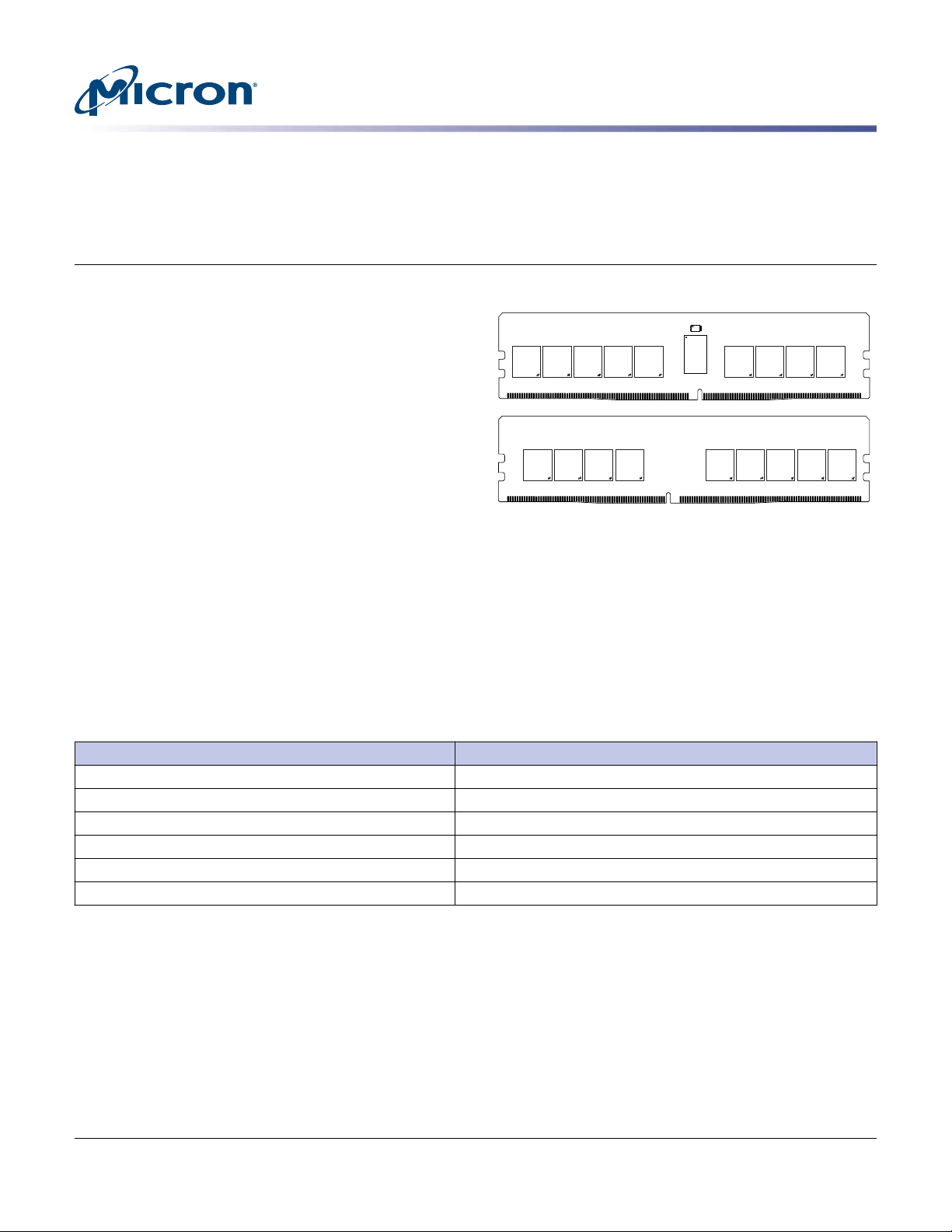
DDR4 SDRAM RDIMM
Primary Side
Secondary Side
U15
U14
U13
U12
U11
U10
U9
U8
U20
U19
U18
U17
U16
U6
U5
U4
U3
U2
U6
U5
U4
U3
U7
U1
U2
Addendum
MTA18ASF4G72PZ – 32GB
32GB (x72, ECC, SR) 288-Pin DDR4 RDIMM
Introduction
Introduction
Information provided here is in addition to or supersedes information provided in the Micron DDR4
RDIMM Core data sheet.
Features
• DDR4 functionality and operations supported as
defined in the component data sheet
• Features and specifications defined in the Micron
DDR4 RDIMM Core data sheet
• 288-pin, registered dual in-line memory module
(RDIMM)
• Fast data transfer rates: PC4-3200, PC4-2933
• 32GB (4 Gig x 72)
• Single-rank
• 16 internal banks; 4 groups of 4 banks each
Table 1: Addressing
Figure 1: 288-Pin RDIMM (MO-309, R/C-C3)
Options Marking
• Operating temperature
– Commercial (0°C ≤ T
• Package
– 288-pin DIMM (halogen-free) Z
• Frequency/CAS latency
– 0.625ns @ CL = 22 (DDR4-3200) -3G2
– 0.682ns @ CL = 21 (DDR4-2933) -2G9
≤ 95°C) None
OPER
Parameter 32GB
Row address 256K A[17:0]
Column address 1K A[9:0]
Device bank group address 4 BG[1:0]
Device bank address per group 4 BA[1:0]
Device configuration 16Gb (4 Gig x 4), 16 banks
Module rank address 1 CS0_n
CCM005-341111752-10523
asf18c4gx72pz.pdf - Rev. C 4/2020 EN
Products and specifications discussed herein are subject to change by Micron without notice.
1
Micron Technology, Inc. reserves the right to change products or specifications without notice.
© 2019 Micron Technology, Inc. All rights reserved.
32GB (x72, ECC, SR) 288-Pin DDR4 RDIMM
Introduction
Table 2: Part Numbers and Timing Parameters – 32GB Modules
Base device: MT40A4G4,1 16Gb DDR4 SDRAM
Part Number
2
Density Configuration
MTA18ASF4G72PZ-3G2__ 32GB 4 Gig x 72 25.6 GB/s 0.625ns/3200 MT/s 22-22-22
MTA18ASF4G72PZ-2G9__ 32GB 4 Gig x 72 23.47 GB/s 0.682/2933 MT/s 21-21-21
Module
Module
Bandwidth
Memory Clock/
Data Rate
Clock Cycles
(CL-nRCD-nRP)
Notes:
1. The data sheet for the base device can be found on micron.com.
2. All part numbers end with a two-place code (not shown) that designates component and PCB revisions.
Consult factory for current revision codes. Example: MTA18ASF4G72PZ-3G2B1.
CCM005-341111752-10523
asf18c4gx72pz.pdf - Rev. C 4/2020 EN
2
Micron Technology, Inc. reserves the right to change products or specifications without notice.
© 2019 Micron Technology, Inc. All rights reserved.

32GB (x72, ECC, SR) 288-Pin DDR4 RDIMM
Important Notes and Warnings
Important Notes and Warnings
Micron Technology, Inc. ("Micron") reserves the right to make changes to information published in this document,
including without limitation specifications and product descriptions. This document supersedes and replaces all
information supplied prior to the publication hereof. You may not rely on any information set forth in this document if you obtain the product described herein from any unauthorized distributor or other source not authorized
by Micron.
Automotive Applications. Products are not designed or intended for use in automotive applications unless specifically designated by Micron as automotive-grade by their respective data sheets. Distributor and customer/distributor shall assume the sole risk and liability for and shall indemnify and hold Micron harmless against all claims,
costs, damages, and expenses and reasonable attorneys' fees arising out of, directly or indirectly, any claim of
product liability, personal injury, death, or property damage resulting directly or indirectly from any use of nonautomotive-grade products in automotive applications. Customer/distributor shall ensure that the terms and conditions of sale between customer/distributor and any customer of distributor/customer (1) state that Micron
products are not designed or intended for use in automotive applications unless specifically designated by Micron
as automotive-grade by their respective data sheets and (2) require such customer of distributor/customer to indemnify and hold Micron harmless against all claims, costs, damages, and expenses and reasonable attorneys'
fees arising out of, directly or indirectly, any claim of product liability, personal injury, death, or property damage
resulting from any use of non-automotive-grade products in automotive applications.
Critical Applications. Products are not authorized for use in applications in which failure of the Micron component could result, directly or indirectly in death, personal injury, or severe property or environmental damage
("Critical Applications"). Customer must protect against death, personal injury, and severe property and environmental damage by incorporating safety design measures into customer's applications to ensure that failure of the
Micron component will not result in such harms. Should customer or distributor purchase, use, or sell any Micron
component for any critical application, customer and distributor shall indemnify and hold harmless Micron and
its subsidiaries, subcontractors, and affiliates and the directors, officers, and employees of each against all claims,
costs, damages, and expenses and reasonable attorneys' fees arising out of, directly or indirectly, any claim of
product liability, personal injury, or death arising in any way out of such critical application, whether or not Micron or its subsidiaries, subcontractors, or affiliates were negligent in the design, manufacture, or warning of the
Micron product.
Customer Responsibility. Customers are responsible for the design, manufacture, and operation of their systems,
applications, and products using Micron products. ALL SEMICONDUCTOR PRODUCTS HAVE INHERENT FAILURE RATES AND LIMITED USEFUL LIVES. IT IS THE CUSTOMER'S SOLE RESPONSIBILITY TO DETERMINE
WHETHER THE MICRON PRODUCT IS SUITABLE AND FIT FOR THE CUSTOMER'S SYSTEM, APPLICATION, OR
PRODUCT. Customers must ensure that adequate design, manufacturing, and operating safeguards are included
in customer's applications and products to eliminate the risk that personal injury, death, or severe property or environmental damages will result from failure of any semiconductor component.
Limited Warranty. In no event shall Micron be liable for any indirect, incidental, punitive, special or consequential
damages (including without limitation lost profits, lost savings, business interruption, costs related to the removal
or replacement of any products or rework charges) whether or not such damages are based on tort, warranty,
breach of contract or other legal theory, unless explicitly stated in a written agreement executed by Micron's duly
authorized representative.
CCM005-341111752-10523
asf18c4gx72pz.pdf - Rev. C 4/2020 EN
3
Micron Technology, Inc. reserves the right to change products or specifications without notice.
© 2019 Micron Technology, Inc. All rights reserved.

DQ Map
Table 3: Component-to-Module DQ Map
32GB (x72, ECC, SR) 288-Pin DDR4 RDIMM
DQ Map
Component
Reference
Number
U2 0 3 157 U3 0 11 168
U4 0 19 179 U5 0 27 190
U6 0 CB3 201 U8 0 35 249
U9 0 43 260 U10 0 51 271
U11 0 59 282 U12 0 60 128
U13 0 52 117 U14 0 44 106
U15 0 36 95 U16 0 CB4 47
U17 0 28 36 U18 0 20 25
U19 0 12 14 U20 0 4 3
Component
DQ Module DQ
1 1 150 1 9 161
2 2 12 2 10 23
3 0 5 3 8 16
1 17 172 1 25 183
2 18 34 2 26 45
3 16 27 3 24 38
1 CB1 194 1 33 242
2 CB2 56 2 34 104
3 CB0 49 3 32 97
1 41 253 1 49 264
2 42 115 2 50 126
3 40 108 3 48 119
1 57 275 1 62 135
2 58 137 2 61 273
3 56 130 3 63 280
1 54 124 1 46 113
2 53 262 2 45 251
3 55 269 3 47 258
1 38 102 1 CB6 54
2 37 240 2 CB5 192
3 39 247 3 CB7 199
1 30 43 1 22 32
2 29 181 2 21 170
3 31 188 3 23 177
1 14 21
2 13 159
3 15 166
Module Pin
Number
Component
Reference
Number
Component
DQ Module DQ
1 6 10
2 5 148
3 7 155
Module Pin
Number
CCM005-341111752-10523
asf18c4gx72pz.pdf - Rev. C 4/2020 EN
4
Micron Technology, Inc. reserves the right to change products or specifications without notice.
© 2019 Micron Technology, Inc. All rights reserved.

32GB (x72, ECC, SR) 288-Pin DDR4 RDIMM
IDD Specifications
IDD Specifications
Table 4: DDR4 IDD Specifications and Conditions – 32GB (Die Revision E)
Values are for the MT40A4G4 DDR4 SDRAM only and are computed from values specified in the 16Gb (4 Gig x 4) component data sheet.
Parameter Symbol 3200 2933 Units
One bank ACTIVATE-PRECHARGE current I
One bank ACTIVATE-PRECHARGE, word line boost, IPP current I
One bank ACTIVATE-READ-PRECHARGE current I
Precharge standby current I
Precharge standby ODT current I
Precharge power-down current I
Precharge quite standby current I
Active standby current I
Active standby IPP current I
Active power-down current I
Burst read current I
Burst write current I
Burst refresh current (1x REF) I
Burst refresh IPP current (1x REF) I
Self refresh current: Normal temperature range (0°C to 85°C) I
Self refresh current: Extended temperature range (0°C to 95°C) I
Self refresh current: Reduced temperature range (0°C to 45°C) I
Auto self refresh current (25°C) I
Auto self refresh current (45°C) I
Auto self refresh current (75°C) I
Auto self refresh current (95°C) I
Auto self refresh IPP current I
Bank interleave read current I
Bank interleave read IPP current I
Maximum power-down current I
DD0
PP0
DD1
DD2N
DD2NT
DD2P
DD2Q
DD3N
PP3N
DD3P
DD4R
DD4W
DD5R
PP5R
DD6N
DD6E
DD6R
DD6A
DD6A
DD6A
DD6A
PP6X
DD7
PP7
DD8
990 972 mA
54 54 mA
1188 1170 mA
900 882 mA
972 954 mA
774 774 mA
846 846 mA
1080 1062 mA
36 36 mA
864 846 mA
2286 2142 mA
1890 1818 mA
1224 1224 mA
72 72 mA
1026 1026 mA
2034 2034 mA
432 432 mA
324 324 mA
432 432 mA
918 918 mA
2034 2034 mA
108 108 mA
4032 3834 mA
162 162 mA
684 684 mA
CCM005-341111752-10523
asf18c4gx72pz.pdf - Rev. C 4/2020 EN
5
Micron Technology, Inc. reserves the right to change products or specifications without notice.
© 2019 Micron Technology, Inc. All rights reserved.

32GB (x72, ECC, SR) 288-Pin DDR4 RDIMM
IDD Specifications
Table 5: DDR4 IDD Specifications and Conditions – 32GB (Die Revision B)
Values are for the MT40A4G4 DDR4 SDRAM only and are computed from values specified in the 16Gb (4 Gig x 4) component data sheet.
Parameter Symbol 3200 2933 Units
One bank ACTIVATE-PRECHARGE current I
One bank ACTIVATE-PRECHARGE, word line boost, IPP current I
One bank ACTIVATE-READ-PRECHARGE current I
Precharge standby current I
Precharge standby ODT current I
Precharge power-down current I
Precharge quite standby current I
Active standby current I
Active standby IPP current I
Active power-down current I
Burst read current I
Burst write current I
Burst refresh current (1x REF) I
Burst refresh IPP current (1x REF) I
Self refresh current: Normal temperature range (0°C to 85°C) I
Self refresh current: Extended temperature range (0°C to 95°C) I
Self refresh current: Reduced temperature range (0°C to 45°C) I
Auto self refresh current (25°C) I
Auto self refresh current (45°C) I
Auto self refresh current (75°C) I
Auto self refresh current (95°C) I
Auto self refresh IPP current I
Bank interleave read current I
Bank interleave read IPP current I
Maximum power-down current I
DD0
PP0
DD1
DD2N
DD2NT
DD2P
DD2Q
DD3N
PP3N
DD3P
DD4R
DD4W
DD5R
PP5R
DD6N
DD6E
DD6R
DD6A
DD6A
DD6A
DD6A
PP6X
DD7
PP7
DD8
1080 1062 mA
72 72 mA
1260 1242 mA
936 918 mA
1008 990 mA
774 774 mA
846 846 mA
1404 1386 mA
54 54 mA
1242 1224 mA
3096 2952 mA
2952 2826 mA
1422 1404 mA
90 90 mA
1206 1206 mA
2178 2178 mA
522 522 mA
180 180 mA
522 522 mA
1098 1098 mA
2178 2178 mA
198 198 mA
4284 4158 mA
198 198 mA
720 720 mA
CCM005-341111752-10523
asf18c4gx72pz.pdf - Rev. C 4/2020 EN
6
Micron Technology, Inc. reserves the right to change products or specifications without notice.
© 2019 Micron Technology, Inc. All rights reserved.

DQ
DQ
DQ
DQ
ZQ
DQ0
DQ1
DQ2
DQ3
Vss
U2
DQ
DQ
DQ
DQ
ZQ
DQ4
DQ5
DQ6
DQ7
Vss
U20
DQS0_t
DQS0_c
DQS9_t
DQS9_c
DQ
DQ
DQ
DQ
ZQ
DQ8
DQ9
DQ10
DQ11
Vss
U3
DQ
DQ
DQ
DQ
ZQ
DQ12
DQ13
DQ14
DQ15
Vss
U19
DQS1_t
DQS1_c
DQS10_t
DQS10_c
DQ
DQ
DQ
DQ
ZQ
DQ16
DQ17
DQ18
DQ19
Vss
U4
DQ
DQ
DQ
DQ
ZQ
DQ20
DQ21
DQ22
DQ23
Vss
U18
DQS2_t
DQS2_c
DQS11_t
DQS11_c
DQ
DQ
DQ
DQ
ZQ
DQ24
DQ25
DQ26
DQ27
Vss
U5
DQ
DQ
DQ
DQ
ZQ
DQ28
DQ29
DQ30
DQ31
Vss
U17
DQS3_t
DQS3_c
DQS12_t
DQS12_c
DQ
DQ
DQ
DQ
ZQ
CB0
CB1
CB2
CB3
Vss
U6
DQ
DQ
DQ
DQ
ZQ
CB4
CB5
CB6
CB7
Vss
U16
DQS8_t
DQS8_c
DQS17_t
DQS17_c
DQ
DQ
DQ
DQ
ZQ
DQ32
DQ33
DQ34
DQ35
Vss
U8
DQ
DQ
DQ
DQ
ZQ
DQ36
DQ37
DQ38
DQ39
Vss
U15
DQS4_t
DQS4_c
DQS13_t
DQS13_c
DQ
DQ
DQ
DQ
ZQ
DQ40
DQ41
DQ42
DQ43
Vss
U9
DQ
DQ
DQ
DQ
ZQ
DQ44
DQ45
DQ46
DQ47
Vss
U14
DQS5_t
DQS5_c
DQS14_t
DQS14_c
DQ
DQ
DQ
DQ
ZQ
DQ48
DQ49
DQ50
DQ51
Vss
U10
DQ
DQ
DQ
DQ
ZQ
DQ52
DQ53
DQ54
DQ55
Vss
U13
DQS6_t
DQS6_c
DQS15_t
DQS15_c
DQ
DQ
DQ
DQ
ZQ
DQ56
DQ57
DQ58
DQ59
Vss
U11
DQ
DQ
DQ
DQ
ZQ
DQ60
DQ61
DQ62
DQ63
Vss
U12
DQS7_t
DQS7_c
DQS16_t
DQS16_c
A/B-CS0_n
U7
A/B-CS0_n, A/B-BA[1:0]A/B-BG[1:0],
A/B-ACT_n, A/B-A[17, 13:0], A/B-RAS_n/A16,
A/B-CAS_n/A15, A/B-WE_n/A14,
A/B-CKE0, A/B-ODT0
CK[1:0]_t
CK[1:0]_c
Command, control, address, and clock line terminations:
DDR4
SDRAM
VTT
DDR4
SDRAM
VDD
U1
A0
SPD EEPROM/
Temperature
sensor
A1 A2
SA0
SA1
SDA
SCL
EVT
EVENT_n
CS_n DQS_t DQS_c
CS_n DQS_t DQS_c
CS_n DQS_t DQS_c
CS_n DQS_t DQS_c
CS_n DQS_t DQS_c
CS_n DQS_t DQS_c
CS_n DQS_t DQS_c
CS_n DQS_t DQS_c
CS_n DQS_t DQS_c
CS_n DQS_t DQS_c
CS_n DQS_t DQS_c
CS_n DQS_t DQS_c
CS_n DQS_t DQS_c
CS_n DQS_t DQS_c
CS_n DQS_t DQS_c
CS_n DQS_t DQS_c
CS_n DQS_t DQS_c
CS_n DQS_t DQS_c
SA2
VREFCA
VSS
DDR4 SDRAM, Register
DDR4 SDRAM, Register
VDD
Control, command and
address termination
VDDSPD
SPD EEPROM/Temp Sensor,
Register
VTT
DDR4 SDRAM, Register
DDR4 SDRAM
VPP
CS0_n
BA[1:0]
BG[1:0]
ACT_n
A[17, 13:0]
RAS_n/A16
CAS_n/A15
WE_n/A14
CKE0
ODT0
PAR_IN
ALERT_CONN_N
A/B-CS0_n: Rank 0
A/B-BA[1:0]: DDR4 SDRAM
A/B-BG[1:0]: DDR4 SDRAM
A/B-ACT_n: DDR4 SDRAM
A/B-A[17,13:0]: DDR4 SDRAM
A/B-RAS_n/A16: DDR4 SDRAM
A/B-CAS_n/A15: DDR4 SDRAM
A/B-WE_n/A14: DDR4 SDRAM
A/B-CKE0: Rank 0
A/B-ODT0: Rank 0
A/B-PAR: DDR4 SDRAM
ALERT_DRAM: DDR4 SDRAM
R
E
G
I
S
T
E
R
&
P
L
L
RESET_N
CK[1:0]_c
DDR4 SDRAM
QRST_N: DDR4 SDRAM
CK[1:0]_t
ZQ
VSS
SA0
SA1
SA2
SCL
SDA
CK0_t
CK0_c
CK1_t
CK1_c
Functional Block Diagram
Figure 2: Functional Block Diagram
CCM005-341111752-10523
asf18c4gx72pz.pdf - Rev. C 4/2020 EN
Note:
1. The ZQ ball on each DDR4 component is connected to an external 240Ω ±1% resistor
32GB (x72, ECC, SR) 288-Pin DDR4 RDIMM
Functional Block Diagram
that is tied to ground. It is used for the calibration of the component’s ODT and output
driver.
7
Micron Technology, Inc. reserves the right to change products or specifications without notice.
© 2019 Micron Technology, Inc. All rights reserved.

32GB (x72, ECC, SR) 288-Pin DDR4 RDIMM
Functional Block Diagram
8000 S. Federal Way, P.O. Box 6, Boise, ID 83707-0006, Tel: 208-368-4000
www.micron.com/products/support Sales inquiries: 800-932-4992
Micron and the Micron logo are trademarks of Micron Technology, Inc.
All other trademarks are the property of their respective owners.
This data sheet contains minimum and maximum limits specified over the power supply and temperature range set forth herein.
Although considered final, these specifications are subject to change, as further product development and data characterization some-
times occur.
CCM005-341111752-10523
asf18c4gx72pz.pdf - Rev. C 4/2020 EN
8
Micron Technology, Inc. reserves the right to change products or specifications without notice.
© 2019 Micron Technology, Inc. All rights reserved.

Mouser Electronics
Authorized Distributor
Click to View Pricing, Inventory, Delivery & Lifecycle Information:
Micron Technology:
MTA18ASF4G72PZ-2G9B1 MTA18ASF4G72PZ-3G2B1 MTA18ASF4G72PZ-2G9E1 MTA18ASF4G72PZ-3G2E1
 Loading...