

Micron MTA18ASF2G72HZ – 16GB User Manual
Module height: 30mm (1.181in)
Module Height: 30mm (1.181 in)
16GB (x72, ECC DR) 260-Pin DDR4 SODIMM
DDR4 SDRAM SODIMM
MTA18ASF2G72HZ – 16GB
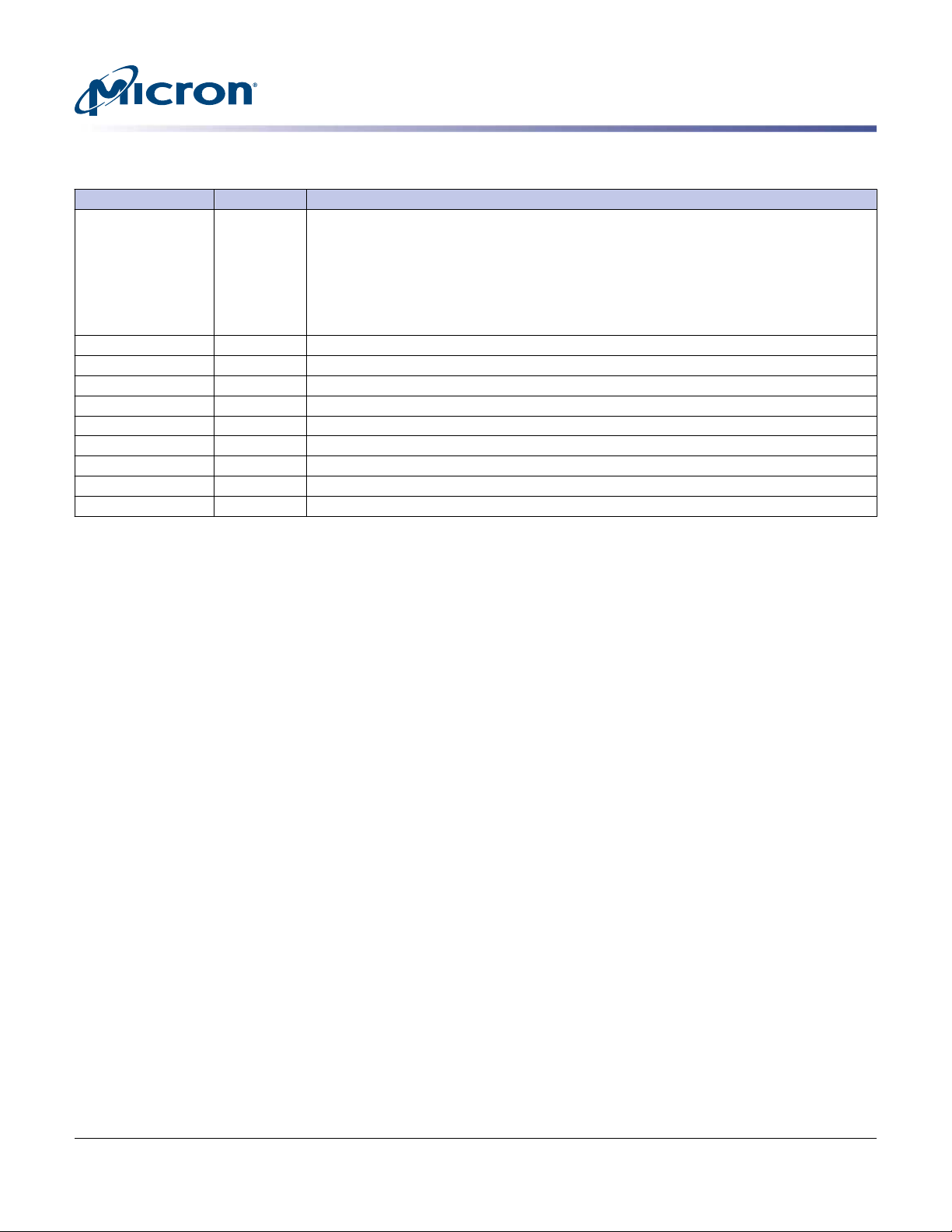
Features
Features
• DDR4 functionality and operations supported as
defined in the component data sheet
• 260-pin, small-outline dual in-line memory module
(SODIMM)
• Fast data transfer rates: PC4-3200, PC4-2666 or
PC4-2400
• 16GB (2 Gig x 72)
• VDD = 1.20V (NOM)
• VPP = 2.5V (NOM)
• V
• Nominal and dynamic on-die termination (ODT) for
data, strobe, and mask signals
• Low-power auto self refresh (LPASR)
• Data bus inversion (DBI) for data bus
• On-die V
• Dual-rank
• On-board I2C temperature sensor with integrated
serial presence-detect (SPD) EEPROM
• 16 internal banks; 4 groups of 4 banks each
• Fixed burst chop (BC) of 4 and burst length (BL) of 8
via the mode register set (MRS)
• Selectable BC4 or BL8 on-the-fly (OTF)
• Gold edge contacts
• Halogen-free
• Fly-by topology
• Terminated control, command, and address bus
= 2.5V (NOM)
DDSPD
generation and calibration
REFDQ
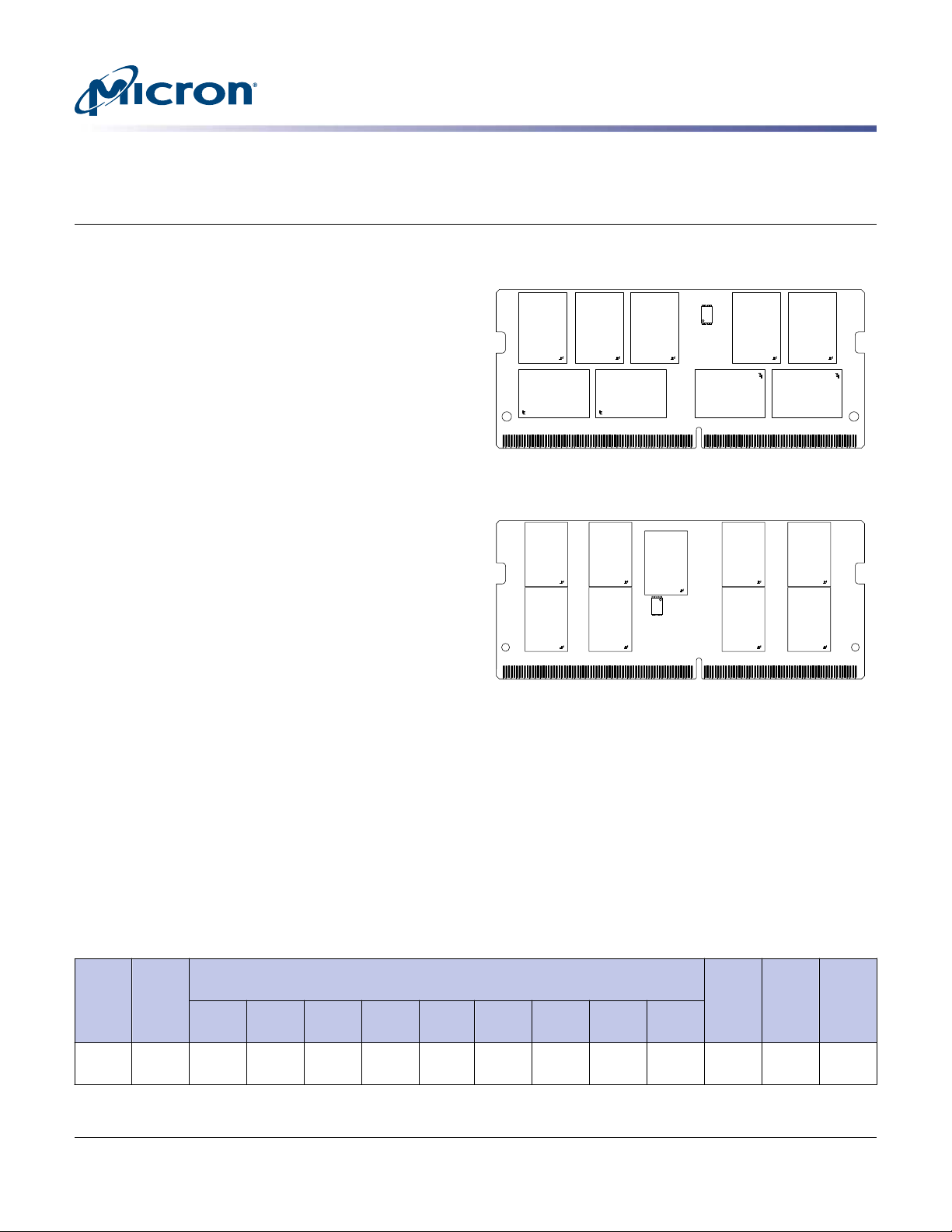
Figure 1: 260-Pin SODIMM (MO-310 R/C H)
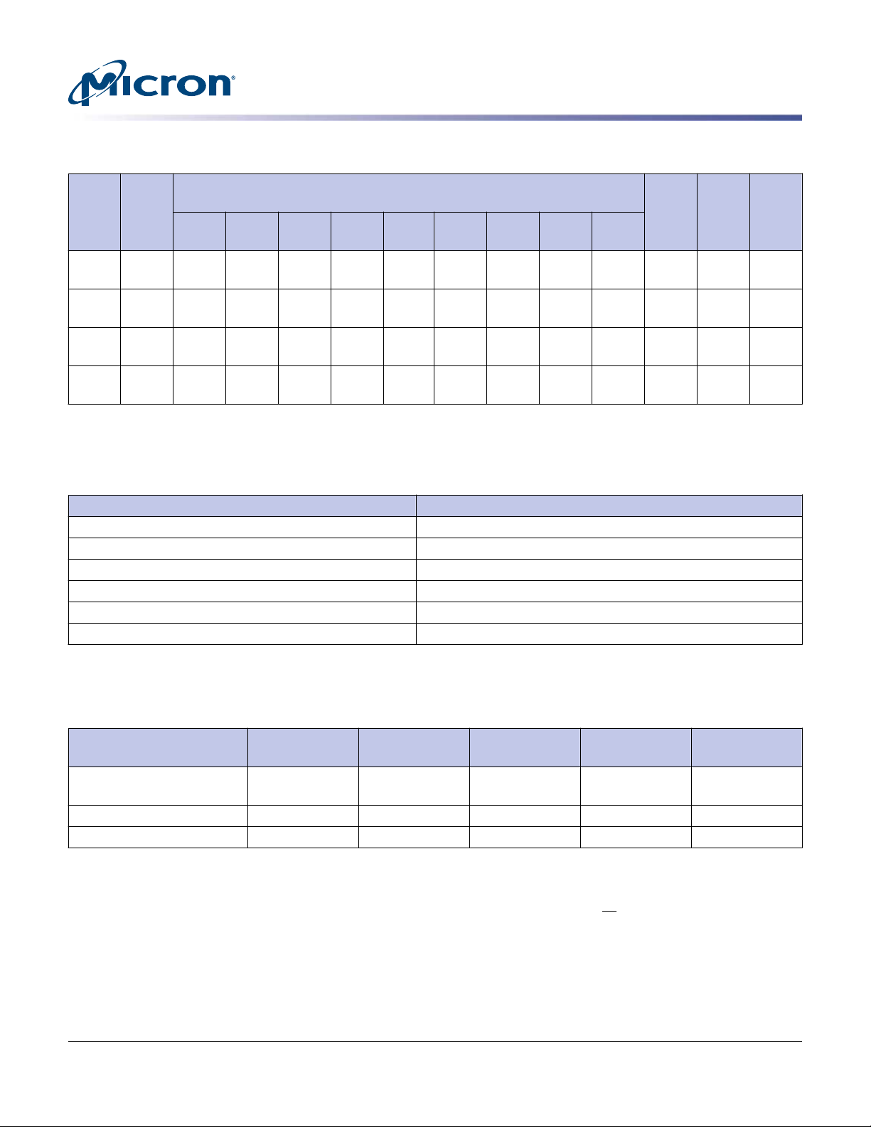
Figure 2: 260-Pin SODIMM (MO-310 R/C G1)
Options Marking
• Operating temperature
– Commercial
(0°C ≤ T
OPER
≤ 95°C)
• Package
– 260-pin DIMM (halogen-free) Z
• Frequency/CAS latency
– 0.62ns @ CL = 22 (DDR4-3200) -3G2
– 0.75ns @ CL = 19 (DDR4-2666) -2G6
– 0.83ns @ CL = 17 (DDR4-2400) -2G3
None
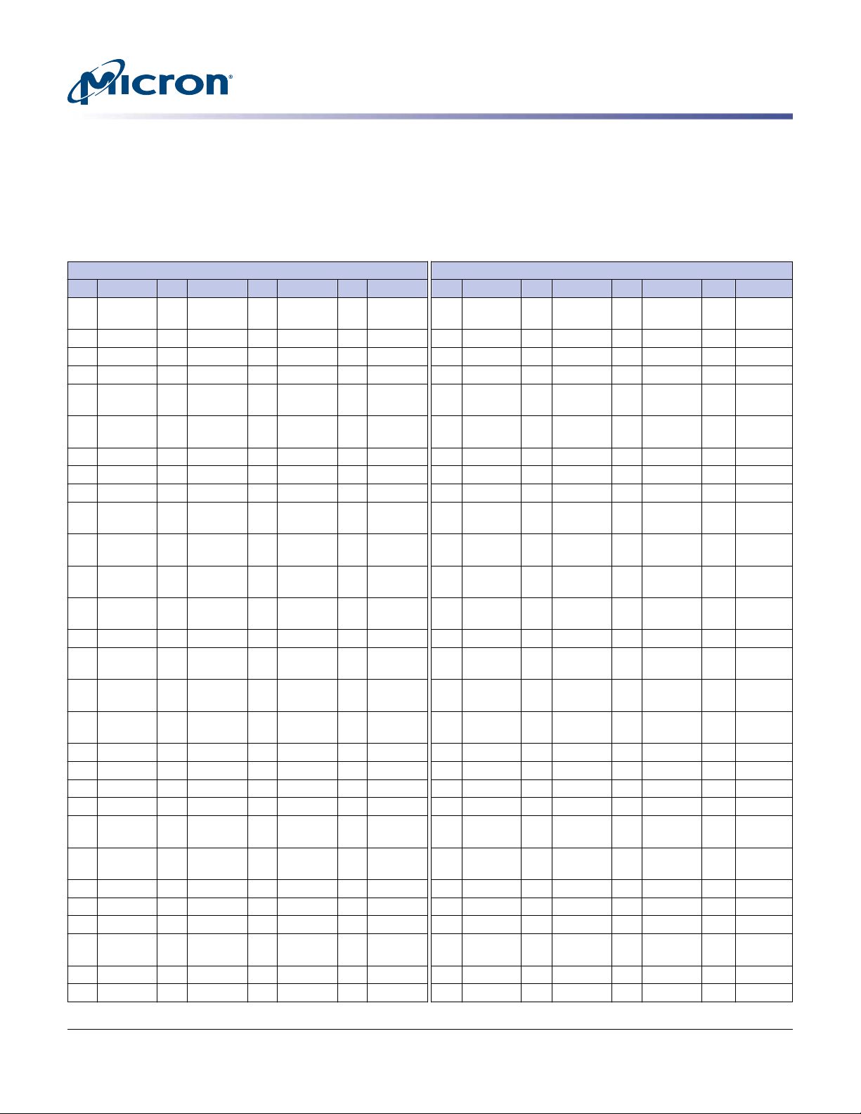
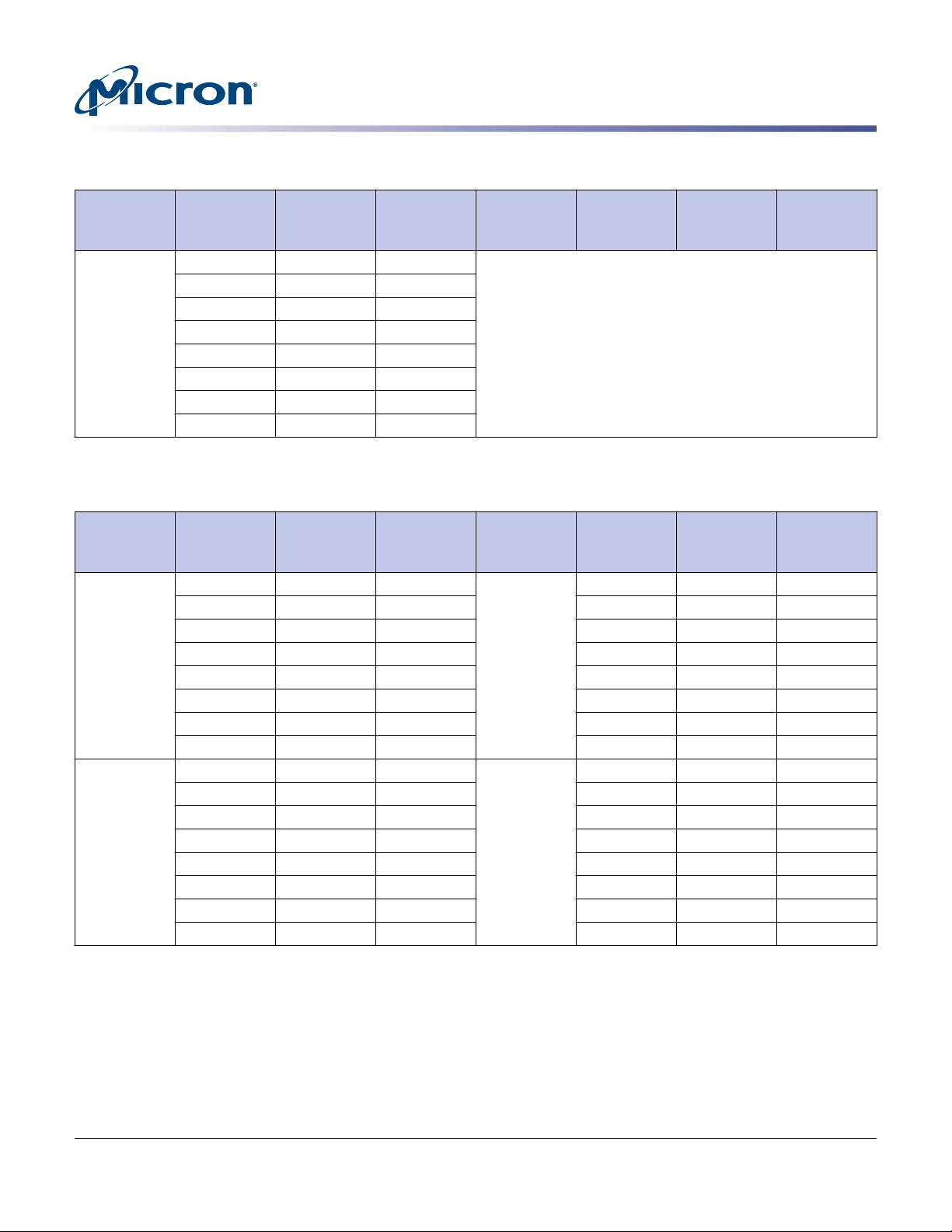
Table 1: Key Timing Parameters
PC4-
Grade
Speed
-3G2 3200 3200,
CCMTD-1725822587-9881
asf18c2gx72hz.pdf – Rev. I 7/20 EN
Products and specifications discussed herein are subject to change by Micron without notice.
2933
3200,
2933
Data Rate (MT/s)
20\
19
2933 2666\
2666
CL =
18\
17
2400\
2400
1
16\
15
2133\
2133
t
14\
13
1866\
1866
Micron Technology, Inc. reserves the right to change products or specifications without notice.
12\
11
1600\
1600
10\
9
1333\–13.75 13.75 45.75
RCD
ns
© 2015 Micron Technology, Inc. All rights reserved.
t
RP
ns
t
RC
ns24 22 21
16GB (x72, ECC DR) 260-Pin DDR4 SODIMM
Table 1: Key Timing Parameters (Continued)
Data Rate (MT/s)
CL =
20\
Grade
Speed
PC4-
19
-2G9 2933 – 2933 2933 2666\
2666
-2G6 2666 – – – 2666\
2666
-2G3 2400 – – – – 2400\
-2G1 2133 – – – – – 2133\
18\
17
2400\
2400
2400\
2400
2400
16\
15
2133\
2133
2133\
2133
2133\
2133
2133
14\
13
1866\
1866
1866\
1866
1866\
1866
1866\
1866
12\
11
1600\
1600
1600\
1600
1600\
1600
1600\
1600
t
10\
9
RCD
ns
1333\–14.32
(13.75)
1333\–14.25
(13.75)
1333\–14.16
(13.75)
1333\
1333
14.06
(13.5)
1
1
1
1
(13.75)
(13.75)
(13.75)
(13.5)
Features
t
RP
ns
14.32
1
14.25
1
14.16
1
14.06
1
t
RC
ns24 22 21
46.32
(45.75)
46.25
(45.75)
46.16
(45.75)
47.06
(46.5)
1
1
1
1
Note:
1. Down-bin timing, refer to component data
sheet Speed Bin Tables for details.
Table 2: Addressing
Parameter 16GB
Row address 64K A[15:0]
Column address 1K A[9:0]
Device bank group address 4 BG[1:0]
Device bank address per group 4 BA[1:0]
Device configuration 8Gb (1Gig x 8), 16 banks
Module rank address CS_n[1:0]
Table 3: Part Numbers and Timing Parameters – 16GB Modules
Base device: MT40A1G8,1 8Gb DDR4 SDRAM
Part Number
MTA18ASF2G72HZ-3G2__
2
Density Configuration
16GB 2 Gig x 72 25.6 GB/s 0.625ns/3200
MTA18ASF2G72HZ-2G6__ 16GB 2 Gig x 72 21.3 GB/s 0.75ns/2666 MT/s 19-19-19
MTA18ASF2G72HZ-2G3__ 16GB 2 Gig x 72 19.2 GB/s 0.83ns/2400 MT/s 17-17-17
Module
Module
Bandwidth
Memory Clock/
Data Rate
MT/s
Clock Cycles
(CL-tRCD-tRP)
22-22-22
Notes:
1. The data sheet for the base device can be found on micron.com.
2. All part numbers end with a two-place code (not shown) that designates component and PCB revisions.
Consult factory for current revision codes. Example: MTA18ASF2G72HZ-3G2E1.
CCMTD-1725822587-9881
asf18c2gx72hz.pdf – Rev. I 7/20 EN
2
Micron Technology, Inc. reserves the right to change products or specifications without notice.
© 2015 Micron Technology, Inc. All rights reserved.

16GB (x72, ECC DR) 260-Pin DDR4 SODIMM
Features
Important Notes and Warnings
Micron Technology, Inc. ("Micron") reserves the right to make changes to information published in this document,
including without limitation specifications and product descriptions. This document supersedes and replaces all
information supplied prior to the publication hereof. You may not rely on any information set forth in this document if you obtain the product described herein from any unauthorized distributor or other source not authorized
by Micron.
Automotive Applications. Products are not designed or intended for use in automotive applications unless specifically designated by Micron as automotive-grade by their respective data sheets. Distributor and customer/distributor shall assume the sole risk and liability for and shall indemnify and hold Micron harmless against all claims,
costs, damages, and expenses and reasonable attorneys' fees arising out of, directly or indirectly, any claim of
product liability, personal injury, death, or property damage resulting directly or indirectly from any use of nonautomotive-grade products in automotive applications. Customer/distributor shall ensure that the terms and conditions of sale between customer/distributor and any customer of distributor/customer (1) state that Micron
products are not designed or intended for use in automotive applications unless specifically designated by Micron
as automotive-grade by their respective data sheets and (2) require such customer of distributor/customer to indemnify and hold Micron harmless against all claims, costs, damages, and expenses and reasonable attorneys'
fees arising out of, directly or indirectly, any claim of product liability, personal injury, death, or property damage
resulting from any use of non-automotive-grade products in automotive applications.
Critical Applications. Products are not authorized for use in applications in which failure of the Micron component could result, directly or indirectly in death, personal injury, or severe property or environmental damage
("Critical Applications"). Customer must protect against death, personal injury, and severe property and environmental damage by incorporating safety design measures into customer's applications to ensure that failure of the
Micron component will not result in such harms. Should customer or distributor purchase, use, or sell any Micron
component for any critical application, customer and distributor shall indemnify and hold harmless Micron and
its subsidiaries, subcontractors, and affiliates and the directors, officers, and employees of each against all claims,
costs, damages, and expenses and reasonable attorneys' fees arising out of, directly or indirectly, any claim of
product liability, personal injury, or death arising in any way out of such critical application, whether or not Micron or its subsidiaries, subcontractors, or affiliates were negligent in the design, manufacture, or warning of the
Micron product.
Customer Responsibility. Customers are responsible for the design, manufacture, and operation of their systems,
applications, and products using Micron products. ALL SEMICONDUCTOR PRODUCTS HAVE INHERENT FAILURE RATES AND LIMITED USEFUL LIVES. IT IS THE CUSTOMER'S SOLE RESPONSIBILITY TO DETERMINE
WHETHER THE MICRON PRODUCT IS SUITABLE AND FIT FOR THE CUSTOMER'S SYSTEM, APPLICATION, OR
PRODUCT. Customers must ensure that adequate design, manufacturing, and operating safeguards are included
in customer's applications and products to eliminate the risk that personal injury, death, or severe property or environmental damages will result from failure of any semiconductor component.
Limited Warranty. In no event shall Micron be liable for any indirect, incidental, punitive, special or consequential
damages (including without limitation lost profits, lost savings, business interruption, costs related to the removal
or replacement of any products or rework charges) whether or not such damages are based on tort, warranty,
breach of contract or other legal theory, unless explicitly stated in a written agreement executed by Micron's duly
authorized representative.
CCMTD-1725822587-9881
asf18c2gx72hz.pdf – Rev. I 7/20 EN
3
Micron Technology, Inc. reserves the right to change products or specifications without notice.
© 2015 Micron Technology, Inc. All rights reserved.
16GB (x72, ECC DR) 260-Pin DDR4 SODIMM
Pin Assignments
Pin Assignments
The pin assignment table below is a comprehensive list of all possible pin assignments
for DDR4 SODIMM modules. See the Functional Block Diagram located in the module
MPN data sheet addendum for pins specific to the module.
Table 4: Pin Assignments
260-Pin DDR4 SODIMM Front 260-Pin DDR4 SODIMM Back
Pin Symbol Pin Symbol Pin Symbol Pin Symbol Pin Symbol Pin Symbol Pin Symbol Pin Symbol
1 V
3 DQ5 69 V
5 V
7 DQ1 73 V
9 V
11 DQS0_c 77 V
13 DQS0_t 79 DQ30 145 BA1 211 DQ52 14 V
15 V
17 DQ7 83 DQ26 149 CS0_n 215 DQ49 18 V
19 V
21 DQ3 87 CB5/NC 153 V
23 V
25 DQ13 91 CB1/NC 157 CS1_n/NC223 V
67 DQ29 133 A1 199 DM5_n/
SS
DBI5_n
135 V
SS
71 DQ25 137 CK0_t 203 DQ46 6 V
SS
139 CK0_c 205 V
SS
SS
75 DM3_n/
141 V
201 V
DD
207 DQ42 10 V
DD
SS
SS
DBI3_n
143 PARITY 209 V
SS
81 V
SS
85 V
SS
SS
SS
147 V
DD
151 WE_n/
213 V
217 V
SS
SS
SS
A14
219 DQS6_c 22 V
DD
89 V
SS
155 ODT0 221 DQS6_t 24 DQ12 90 V
SS
SS
2 V
4 DQ4 70 DQ24 136 V
SS
SS
68 V
72 V
134 EVENT_n,NF200 DQS5_t
SS
DD
138 CK1_t/NF 204 DQ47
SS
202 V
8 DQ0 74 DQS3_c 140 CK1_c/NF 206 V
SS
12 DM0_n/
76 DQS3_t 142 V
78 V
144 A0 210 V
SS
DD
208 DQ43
DBI0_n
80 DQ31 146 A10/AP 212 DQ53
SS
16 DQ6 82 V
84 DQ27 150 BA0 216 DQ48
SS
20 DQ2 86 V
SS
SS
148 V
DD
152 RAS_n/
214 V
218 V
A16
88 CB4/NC 154 V
SS
SS
156 CAS_n/
DD
220 DM6_n/
222 V
A15
26 V
92 CB0/NC 158 A13 224 DQ54
SS
DBI6_n
SS
SS
SS
SS
SS
SS
27 V
29 DQ9 95 DQS8_c/NC161 ODT1/NC227
31 V
33 DM1_n/
93 V
SS
97 DQS8_t/NC163 V
SS
99 V
159 V
SS
165 C1, CS3_n,NC231 V
SS
DD
DD
225 DQ55 28 DQ8 94 V
V
SS
30 V
229 DQ51 32 DQS1_c 98 V
SS
34 DQS1_t 100 CB6/NC 166 SA2 232 DQ60
DBI_n
35 V
37 DQ15 103 V
39 V
41 DQ10 107 V
43 V
101 CB2/NC 167 V
SS
SS
105 CB3/NC 171 V
SS
SS
109 CKE0 175 V
SS
233 DQ61 36 V
SS
169 DQ37 235 V
237 DQ56 40 V
SS
173 DQ33 239 V
241 DM7_n/
SS
SS
SS
38 DQ14 104 CB7/NC 170 DQ36 236 DQ57
42 DQ11 108 RESET_n 174 DQ32 240 DQS7_c
44 V
DBI7_n
45 DQ21 111 V
47 V
113 BG1 179 DQS4_t 245 DQ62 48 V
SS
49 DQ17 115 BG0 181 V
51 V
SS
117 V
53 DQS2_c 119 A12 185 V
177 DQS4_c 243 V
DD
247 V
SS
183 DQ38 249 DQ58 52 V
DD
251 V
SS
SS
SS
SS
46 DQ20 112 V
50 DQ16 116 ALERT_n 182 DQ39 248 V
54 DM2_n/
55 DQS2_t 121 A9 187 DQ34 253 SCL 56 V
57 V
CCMTD-1725822587-9881
asf18c2gx72hz.pdf – Rev. I 7/20 EN
SS
123 V
DD
189 V
255 V
SS
DDSPD
58 DQ22 124 V
4
SS
96 DM8_n/
SS
DBI_n/NC
SS
102 V
SS
106 V
SS
110 CKE1/NC176 V
SS
SS
SS
DD
160 V
162 C0/
CS2_n/NC
164 V
REFCA
168 V
172 V
178 DM4_n/
DD
SS
SS
SS
226 V
228 DQ50
230 V
234 V
238 V
242 DQS7_t
244 V
DBI4_n
114 ACT_n 180 V
SS
118 V
SS
DD
184 V
SS
SS
246 DQ63
250 DQ59
120 A11 186 DQ35 252 V
DBI2_n
122 A7 188 V
SS
190 DQ45 256 SA0
DD
Micron Technology, Inc. reserves the right to change products or specifications without notice.
© 2015 Micron Technology, Inc. All rights reserved.
SS
254 SDA
SS
SS
SS
SS
SS
SS
SS

16GB (x72, ECC DR) 260-Pin DDR4 SODIMM
Pin Assignments
Table 4: Pin Assignments (Continued)
260-Pin DDR4 SODIMM Front 260-Pin DDR4 SODIMM Back
Pin Symbol Pin Symbol Pin Symbol Pin Symbol Pin Symbol Pin Symbol Pin Symbol Pin Symbol
59 DQ23 125 A8 191 DQ44 257 V
61 V
63 DQ19 129 V
65 V
127 A6 193 V
SS
DD
131 A3 197 V
SS
259 V
SS
195 DQ40 – – 64 V
SS
– – 66 DQ28 132 A2 198 DQS5_c – –
PP
PP
60 V
126 A5 192 V
SS
SS
258 V
62 DQ18 128 A4 194 DQ41 260 SA1
SS
130 V
DD
196 V
SS
– –
TT
CCMTD-1725822587-9881
asf18c2gx72hz.pdf – Rev. I 7/20 EN
5
Micron Technology, Inc. reserves the right to change products or specifications without notice.
© 2015 Micron Technology, Inc. All rights reserved.
16GB (x72, ECC DR) 260-Pin DDR4 SODIMM
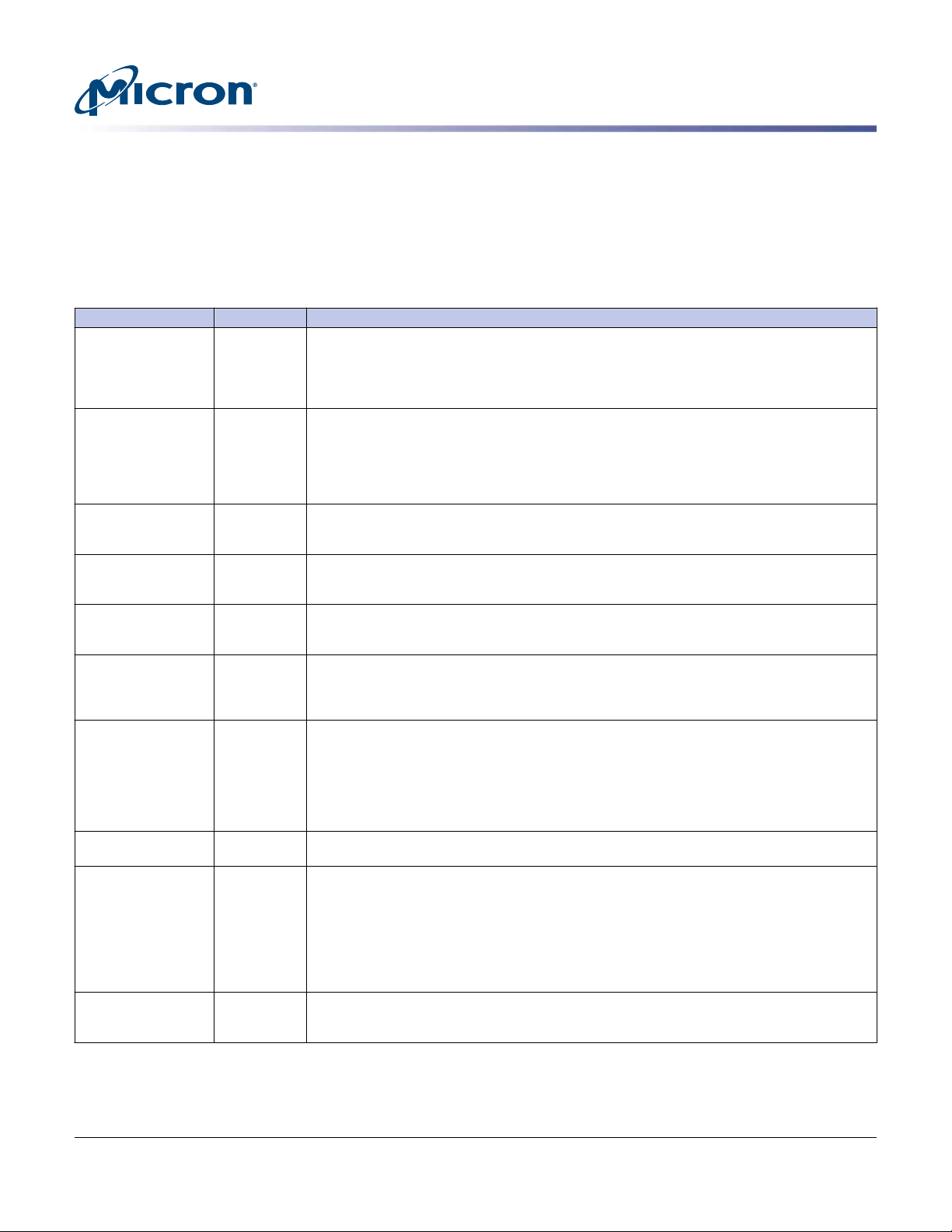
Pin Descriptions
Pin Descriptions
The pin description table below is a comprehensive list of all possible pins for DDR4
modules. All pins listed may not be supported on this module. See the Functional Block
Diagram located in the module MPN data sheet addendum for pins specific to the module.
Table 5: Pin Descriptions
Symbol Type Description
Ax Input Address inputs: Provide the row address for ACTIVATE commands and the column address for
A10/AP Input Auto precharge: A10 is sampled during READ and WRITE commands to determine whether an
A12/BC_n Input Burst chop: A12/BC_n is sampled during READ and WRITE commands to determine if burst
ACT_n Input Command input: ACT_n defines the ACTIVATE command being entered along with CS_n. The
BAx Input Bank address inputs: Define the bank (with a bank group) to which an ACTIVATE, READ,
BGx Input Bank group address inputs: Define the bank group to which a REFRESH, ACTIVATE, READ,
C0, C1, C2
(RDIMM/LRDIMM on-
ly)
CKx_t
CKx_c
CKEx Input Clock enable: CKE HIGH activates and CKE LOW deactivates the internal clock signals, device
CSx_n Input Chip select: All commands are masked when CS_n is registered HIGH. CS_n provides external
Input Chip ID: These inputs are used only when devices are stacked; that is, 2H, 4H, and 8H stacks for
Input Clock: Differential clock inputs. All address, command, and control input signals are sampled
READ/WRITE commands in order to select one location out of the memory array in the respective bank (A10/AP, A12/BC_n, WE_n/A14, CAS_n/A15, and RAS_n/A16 have additional functions;
see individual entries in this table). The address inputs also provide the op-code during the
MODE REGISTER SET command. A17 is only defined for x4 SDRAM.
auto precharge should be performed on the accessed bank after a READ or WRITE operation
(HIGH = auto precharge; LOW = no auto precharge). A10 is sampled during a PRECHARGE command to determine whether the precharge applies to one bank (A10 LOW) or all banks (A10
HIGH). If only one bank is to be precharged, the bank is selected by the bank group and bank
addresses.
chop (on-the-fly) will be performed (HIGH = no burst chop; LOW = burst chopped). See Command Truth Table in the DDR4 component data sheet.
input into RAS_n/A16, CAS_n/A15, and WE_n/A14 are considered as row address A16, A15, and
A14. See Command Truth Table.
WRITE, or PRECHARGE command is being applied. Also determine which mode register is to be
accessed during a MODE REGISTER SET command.
WRITE, or PRECHARGE command is being applied. Also determine which mode register is to be
accessed during a MODE REGISTER SET command. BG[1:0] are used in the x4 and x8 configurations. x16-based SDRAM only has BG0.
x4 and x8 configurations using through-silicon vias (TSVs). These pins are not used in the x16
configuration. Some DDR4 modules support a traditional DDP package, which uses CS1_n,
CKE1, and ODT1 to control the second die. All other stack configurations, such as a 4H or 8H,
are assumed to be single-load (master/slave) type configurations where C0, C1, and C2 are used
as chip ID selects in conjunction with a single CS_n, CKE, and ODT. Chip ID is considered part of
the command code.
on the crossing of the positive edge of CK_t and the negative edge of CK_c.
input buffers, and output drivers. Taking CKE LOW provides PRECHARGE POWER-DOWN and
SELF REFRESH operations (all banks idle), or active power-down (row active in any bank). CKE is
asynchronous for self refresh exit. After V
tialization sequence, it must be maintained during all operations (including SELF REFRESH). CKE
must be maintained HIGH throughout read and write accesses. Input buffers (excluding CK_t,
CK_c, ODT, RESET_n, and CKE) are disabled during power-down. Input buffers (excluding CKE
and RESET_n) are disabled during self refresh.
rank selection on systems with multiple ranks. CS_n is considered part of the command code
(CS2_n and CS3_n are not used on UDIMMs).
has become stable during the power-on and ini-
REFCA
CCMTD-1725822587-9881
asf18c2gx72hz.pdf – Rev. I 7/20 EN
6
Micron Technology, Inc. reserves the right to change products or specifications without notice.
© 2015 Micron Technology, Inc. All rights reserved.

16GB (x72, ECC DR) 260-Pin DDR4 SODIMM
Pin Descriptions
Table 5: Pin Descriptions (Continued)
Symbol Type Description
ODTx Input On-die termination: ODT (registered HIGH) enables termination resistance internal to the
PARITY Input Parity for command and address: This function can be enabled or disabled via the mode
RAS_n/A16
Input Command inputs: RAS_n/A16, CAS_n/A15, and WE_n/A14 (along with CS_n) define the com-
CAS_n/A15
WE_n/A14
RESET_n CMOS Input Active LOW asynchronous reset: Reset is active when RESET_n is LOW and inactive when RE-
SAx Input
SCL Input
DQx, CBx I/O Data input/output and check bit input/output: Bidirectional data bus. DQ represents
DM_n/DBI_n/
I/O Input data mask and data bus inversion: DM_n is an input mask signal for write data. Input
TDQS_t (DMU_n,
DBIU_n), (DML_n/
DBIl_n)
SDA I/O Serial Data: Bidirectional signal used to transfer data in or out of the EEPROM or EEPROM/TS
DQS_t
I/O Data strobe: Output with read data, input with write data. Edge-aligned with read data, cen-
DQS_c
DQSU_t
DQSU_c
DQSL_t
DQSL_c
ALERT_n Output Alert output: Possesses functions such as CRC error flag and command and address parity error
EVENT_n Output Temperature event: The EVENT_n pin is asserted by the temperature sensor when critical tem-
DDR4 SDRAM. When enabled, ODT (RTT) is applied only to each DQ, DQS_t, DQS_c, DM_n/
DBI_n/TDQS_t, and TDQS_c signal for x4 and x8 configurations (when the TDQS function is enabled via the mode register). For the x16 configuration, RTT is applied to each DQ, DQSU_t,
DQSU_c, DQSL_t, DQSL_c, UDM_n, and LDM_n signal. The ODT pin will be ignored if the mode
registers are programmed to disable RTT.
register. When enabled in MR5, the DRAM calculates parity with ACT_n, RAS_n/A16, CAS_n/A15,
WE_n/A14, BG[1:0], BA[1:0], A[16:0]. Input parity should be maintained at the rising edge of the
clock and at the same time as command and address with CS_n LOW.
mand and/or address being entered and have multiple functions. For example, for activation
with ACT_n LOW, these are addresses like A16, A15, and A14, but for a non-activation command with ACT_n HIGH, these are command pins for READ, WRITE, and other commands defined in Command Truth Table.
SET_n is HIGH. RESET_n must be HIGH during normal operation.
Serial address inputs: Used to configure the temperature sensor/SPD EEPROM address range
on the I2C bus.
Serial clock for temperature sensor/SPD EEPROM: Used to synchronize communication to
and from the temperature sensor/SPD EEPROM on the I2C bus.
DQ[3:0], DQ[7:0], and DQ[15:0] for the x4, x8, and x16 configurations, respectively. If cyclic redundancy checksum (CRC) is enabled via the mode register, the CRC code is added at the end of
the data burst. Any one or all of DQ0, DQ1, DQ2, or DQ3 may be used for monitoring of internal V
level during test via mode register setting MR[4] A[4] = HIGH; training times change
REF
when enabled.
data is masked when DM_n is sampled LOW coincident with that input data during a write access. DM_n is sampled on both edges of DQS. DM is multiplexed with the DBI function by the
mode register A10, A11, and A12 settings in MR5. For a x8 device, the function of DM or TDQS
is enabled by the mode register A11 setting in MR1. DBI_n is an input/output identifying
whether to store/output the true or inverted data. If DBI_n is LOW, the data will be stored/
output after inversion inside the DDR4 device and not inverted if DBI_n is HIGH. TDQS is only
supported in x8 SDRAM configurations (TDQS is not valid for UDIMMs).
combo device.
tered-aligned with write data. For x16 configurations, DQSL corresponds to the data on
DQ[7:0], and DQSU corresponds to the data on DQ[15:8]. For the x4 and x8 configurations, DQS
corresponds to the data on DQ[3:0] and DQ[7:0], respectively. DDR4 SDRAM supports a differential data strobe only and does not support a single-ended data strobe.
flag as output signal. If a CRC error occurs, ALERT_n goes LOW for the period time interval and
returns HIGH. If an error occurs during a command address parity check, ALERT_n goes LOW until the on-going DRAM internal recovery transaction is complete. During connectivity test mode,
this pin functions as an input. Use of this signal is system-dependent. If not connected as signal,
ALERT_n pin must be connected to VDD on DIMMs.
perature thresholds have been exceeded. This pin has no function (NF) on modules without
temperature sensors.
CCMTD-1725822587-9881
asf18c2gx72hz.pdf – Rev. I 7/20 EN
7
Micron Technology, Inc. reserves the right to change products or specifications without notice.
© 2015 Micron Technology, Inc. All rights reserved.
16GB (x72, ECC DR) 260-Pin DDR4 SODIMM
Table 5: Pin Descriptions (Continued)
Symbol Type Description
TDQS_t
TDQS_c
(x8 DRAM-based
RDIMM only)
V
DD
V
PP
V
REFCA
V
SS
V
TT
V
DDSPD
RFU – Reserved for future use.
NC – No connect: No internal electrical connection is present.
NF – No function: May have internal connection present, but has no function.
Output Termination data strobe: When enabled via the mode register, the DRAM device enables the
same RTT termination resistance on TDQS_t and TDQS_c that is applied to DQS_t and DQS_c.
When the TDQS function is disabled via the mode register, the DM/TDQS_t pin provides the data mask (DM) function, and the TDQS_c pin is not used. The TDQS function must be disabled in
the mode register for both the x4 and x16 configurations. The DM function is supported only in
x8 and x16 configurations. DM, DBI, and TDQS are a shared pin and are enabled/disabled by
mode register settings. For more information about TDQS, see the DDR4 DRAM component data sheet (TDQS_t and TDQS_c are not valid for UDIMMs).
Supply Module power supply: 1.2V (TYP).
Supply DRAM activating power supply: 2.5V –0.125V/+0.250V.
Supply Reference voltage for control, command, and address pins.
Supply Ground.
Supply Power supply for termination of address, command, and control VDD/2.
Supply Power supply used to power the I2C bus for SPD.
Pin Descriptions
CCMTD-1725822587-9881
asf18c2gx72hz.pdf – Rev. I 7/20 EN
8
Micron Technology, Inc. reserves the right to change products or specifications without notice.
© 2015 Micron Technology, Inc. All rights reserved.

16GB (x72, ECC DR) 260-Pin DDR4 SODIMM
DQ Maps
Table 6: Component-to-Module DQ Map R/C-H (PCB 1813), Front
DQ Maps
Component
Reference
Number
Component
DQ Module DQ
Module Pin
Number
Component
Reference
Number
Component
DQ Module DQ
U1 0 14 38 U2 0 31 80
1 12 24 1 28 66
2 15 37 2 30 79
3 13 25 3 29 67
4 11 42 4 27 84
5 8 28 5 24 70
6 10 41 6 26 83
7 9 29 7 25 71
U3 0 CB3 105 U5 0 39 182
1 CB0 92 1 36 170
2 CB2 101 2 38 183
3 CB1 91 3 37 169
4 CB7 104 4 35 186
5 CB4 88 5 32 174
6 CB6 100 6 34 187
7 CB5 87 7 33 173
U6 0 54 224 U7 0 7 17
1 53 212 1 5 3
2 55 225 2 6 16
3 52 211 3 4 4
4 50 228 4 2 20
5 48 216 5 0 8
6 51 229 6 3 21
7 49 215 7 1 7
U8 0 23 59 U9 0 42 207
1 21 45 1 41 194
2 22 58 2 43 208
3 20 46 3 40 195
4 19 63 4 47 204
5 16 50 5 45 190
6 18 62 6 46 203
7 17 49 7 44 191
Module Pin
Number
CCMTD-1725822587-9881
asf18c2gx72hz.pdf – Rev. I 7/20 EN
9
Micron Technology, Inc. reserves the right to change products or specifications without notice.
© 2015 Micron Technology, Inc. All rights reserved.
16GB (x72, ECC DR) 260-Pin DDR4 SODIMM
Table 6: Component-to-Module DQ Map R/C-H (PCB 1813), Front (Continued)
DQ Maps
Component
Reference
Number
Component
DQ Module DQ
Module Pin
Number
Component
Reference
Number
Component
DQ Module DQ
U10 0 58 249
1 56 237
2 59 250
3 57 236
4 63 246
5 61 233
6 62 245
7 60 232
Table 7: Component-to-Module DQ Map R/C-H (PCB 1813), Back
Component
Reference
Number
Component
DQ Module DQ
Module Pin
Number
U11 0 53 212 U12 0 36 170
1 54 224 1 39 182
2 52 211 2 37 169
3 55 225 3 38 183
4 48 216 4 32 174
5 50 228 5 35 186
6 49 215 6 33 173
7 51 229 7 34 187
U13 0 CB0 92 U14 0 28 66
1 CB3 105 1 31 80
2 CB1 91 2 29 67
3 CB2 101 3 30 79
4 CB4 88 4 24 70
5 CB7 104 5 27 84
6 CB5 87 6 25 71
7 CB6 100 7 26 83
Component
Reference
Number
Component
DQ Module DQ
Module Pin
Number
Module Pin
Number
CCMTD-1725822587-9881
asf18c2gx72hz.pdf – Rev. I 7/20 EN
10
Micron Technology, Inc. reserves the right to change products or specifications without notice.
© 2015 Micron Technology, Inc. All rights reserved.
 Loading...