

Page 1
MT9V125: 1/4-Inch VGA SOC Digital Image Sensor
Features
1/4-Inch System-On-A-Chip (SOC) VGA
NTSC and PAL CMOS Digital Image Sensor
MT9V125
For the latest data sheet, refer to Micron’s Web site: www.micron.com/imaging
Features
•Micron® DigitalClarity® CMOS imaging technology
• Superior low-light performance
• System-on-a-chip (SOC)—completely integrated
camera system
• Supports use of external devices for addition of
custom overlay graphics
• NTSC/PAL (true two-field) analog composite video
output
• ITU-R BT.656 parallel output (8-bit, interlaced)
• Simultaneous composite and digital video outputs
Serial LVDS data output
• Image flow processor (IFP) for sophisticated
processing
• Color recovery and correction, sharpening, gamma,
lens shading correction, and on-the-fly defect
correction
• Automatic features:
• auto exposure, auto white balance (AWB), auto black
reference (ABR), auto flicker avoidance, auto color
saturation, and auto defect identification and
correction
•Simple two-wire serial programming interface
• Low power, interlaced scan CMOS image sensor
Applications
• Automotive
– Rear view camera
– Side mirror replacement
– Blind spot view
– Occupant monitoring
Table 1: Key Performance Parameters
Parameter Value
Optical format 1/4-inch (4:3)
Active imager size 3.63mm(H) x 2.78mm(V)
4.57mm diagonal
Active pixels 640H x 480V
NTSC output 720H x 486V
PAL output 720H x 576V
Pixel size 5.6µm x 5.6µm
Color filter array RGB paired Bayer pattern
Shutter type Electronic rolling shutter (ERS)
Maximum data rate/
master clock
Frame rate – VGA (640H
x 480V)
Integration time
(composite video)
ADC resolution 10-bit, on-chip
Responsivity 5 V/lux-s (550nm)
Pixel dynamic range 70dB
SNR
MAX
Supply
voltage
Power
consumption
Operating temperature –40°C to +105°C
Packaging 52-ball iBGA
I/O digital 2.5–3.1V (2.8V nominal)
Core
digital
Analog 2.5–3.1V (2.8V nominal)
Operating 320mW
Standby 0.56mW
13.5 Mp/s,
27 MHz
30 fps at 27 MHz (NTSC)
25 fps at 27 MHz (PAL)
16µs–33ms (NTSC)
16µs–40ms (PAL)
39dB
2.5–3.1V (2.8V nominal)
Ordering Information
Table 2: Available Part Numbers
Part Number Description
Data Sheet Applicable to Silicon Revision: Rev4
PDF: 09005aef829db8a0/Source: 09005aef829dbfdb Micron Technology, Inc., reserves the right to change products or specifications without notice.
MT9V125_LDS_1.fm - Rev. A 4/07 EN
Products and specifications discussed herein are subject to change by Micron without notice.
MT9V125IA7XTC 52-Ball iBGA (Pb-free)
MT9V125I77XTC 52-Ball iBGA
MT9V125D00XTC K12BC1 Bare die
MT9V125IA7XTCD ES Demo kit (Pb-free)
MT9V125IA7XTCH ES Headboard (Pb-free)
MT9V125IA7XTCR ES Reference camera (Pb-free)
1 ©2007 Micron Technology, Inc. All rights reserved.
Page 2
General Description
0
10
20
30
40
50
60
350 450 550 650 750 850 950 1050
Rev4 Blue
Rev4 Green
Rev4 Red
Quantum Efficiency [%]
Wavelength [nm]
The MT9V125 is a VGA CMOS image sensor featuring Micron’s breakthrough DigitalClarity technology—a low-noise CMOS imaging technology that achieves CCD image quality
(based on signal-to-noise ratio and low-light sensitivity) while maintaining the inherent
size, cost, low power, and integration advantages of CMOS.
The MT9V125 performs sophisticated processing functions including color recovery,
color correction, sharpening, programmable gamma correction, auto black reference
clamping, auto exposure, automatic 50Hz/60Hz flicker avoidance, lens shading correction, auto white balance (AWB), and on-the-fly defect identification and correction.
The MT9V125 outputs interlaced-scan images at 30 or 25 fps, supporting both NTSC and
PAL video formats.
The MT9V125 also includes digital video output that can be switched to the NTSC/PAL
encoder. This can be used in conjunction with an external digital signal processor (DSP)
to provide an overlay (such as a steering aid) on top of the live video.
The image data can be output on any one of three output ports:
• Composite analog video (single-ended and differential support)
• Low-voltage differential signaling (LVDS)
• CCIR 656 interlaced digital video in parallel 8-bit format
MT9V125: 1/4-Inch VGA SOC Digital Image Sensor
General Description
Table 3: MT9V125 Detailed Performance Parameters
Parameter Val ue
Effective fill factor (with microlens)
Output gain
Read noise
Dark current
Figure 1: Quantum Efficiency vs. Wavelength
TBD
28 e-/LSB
6 e-RMS at 16X
119 e-/pix/s at 55°C
PDF: 09005aef829db8a0/Source: 09005aef829dbfdb Micron Technology, Inc., reserves the right to change products or specifications without notice.
MT9V125_LDS_2.fm - Rev. A 4/07 EN
2 ©2007 Micron Technology, Inc. All rights reserved.
Page 3
Functional Overview
SRAM
Line Buffers
Image Flow Processor
Colorpipe
Image Flow Processor
Camera Control
Image Data
Control Bus
Pixel Data
SCLK
S
DATA
EXTCLK
STANDBY
V
DD
/
DGND
V AA / AGND
VAAPIX
Lens shading correction
Color interpolation
Defect correction
Color correction
Gamma correction
Color conversion + formatting
Auto exposure
Auto white balance
Flicker detect/avoid
D OUT[7:0]
PIXCLK
FRAME_VALID
LINE_VALID
Control Bus
Sensor control
(gains, shutter, etc.)
Sensor Core
640H x 480V
1/4-inch optical format
True Interlaced Readout
Auto black compensation
Programmable analog gain
Programmable exposure
10-bit ADC
Control Bus
NTSC and PAL
Encoder
and DAC
LVDS Formatter
and Driver
LVD S_OUT_POS
LVD S_OUT_NEG
DAC_OUT_POS
DAC_OUT_NEG
D
IN[7:0]
DIN_CLK
Horizontal interpolator
8
The MT9V125 is a fully-automatic, single-chip camera, requiring only a single power
supply, lens, and clock source for basic operation. Output video is streamed via the chosen output port. The MT9V125 internal registers are configured using a two-wire serial
interface.
The device can be put into a low-power sleep mode by asserting STANDBY and shutting
down the clock. Output signals can be tri-stated. Both tri-stating output signals and
entry into standby mode can be achieved via two-wire serial interface register writes.
The MT9V125 requires an input clock of 27 MHz to support correct NTSC or PAL timing.
Internal Architecture
Internally, the MT9V125 consists of a sensor core and an image flow processor (IFP). The
IFP is divided in two sections, the color pipe and the camera controller. The sensor core
captures raw images that are then input into the IFP. The color pipe section processes
the incoming stream to create interpolated, color-corrected output, and the camera
controller section controls the sensor core to maintain the desired exposure and color
balance.
The IFP scales the image and an integrated video encoder generates either NTSC or PAL
analog composite output. The MT9V125 supports three different output ports; analog
composite video out, LVDS serial out and CCIR 656 interlaced digital video in parallel 8bit format.
Figure 2 shows the major functional blocks of the MT9V125. The built-in NTSC/PAL
encoder and the LVDS formatter allow simultaneous outputs of composite and digital
video signals.
MT9V125: 1/4-Inch VGA SOC Digital Image Sensor
Functional Overview
Figure 2: Functional Block Diagram
PDF: 09005aef829db8a0/Source: 09005aef829dbfdb Micron Technology, Inc., reserves the right to change products or specifications without notice.
MT9V125_LDS_2.fm - Rev. A 4/07 EN
3 ©2007 Micron Technology, Inc. All rights reserved.
Page 4
MT9V125: 1/4-Inch VGA SOC Digital Image Sensor
DSP
Image
Sensor
Parallel
digital
signal with
overlay
(CCIR 656)
NTSC or PAL composite analog output with overlay
D
IN
[7:0]
D
OUT
[7:0]
DIN_CLK
Parallel
digital
(CCIR 656)
PIXCLK
27 MHz
Oscillator
Figure 3 shows a typical application using a DSP to produce a video overlay (such as a
steering aid). The parallel digital video output is sent to the DSP, which adds the overlay.
The digital video with the overlay is then looped back into the MT9V125 to the NTSC/
PAL encoder and LVDS formatter to provide simultaneous composite analog and digital
LVD S ou t pu t s.
Figure 3: Typical Usage Configuration with Overlay
Functional Overview
PDF: 09005aef829db8a0/Source: 09005aef829dbfdb Micron Technology, Inc., reserves the right to change products or specifications without notice.
MT9V125_LDS_2.fm - Rev. A 4/07 EN
4 ©2007 Micron Technology, Inc. All rights reserved.
Page 5
MT9V125: 1/4-Inch VGA SOC Digital Image Sensor
A
GND
0.1µF
0.1µF
V
AA
D
GND
1µF
V
DD
VAAPIX
1µF
A
GND
0.1µF
1µF
VDD
Power
V
AA AND
VAAPIX
5
Power
10µF
1.5KΩ2 1.5KΩ
2
S
DATA
SCLK
RESET_BAR
LVDS_ENABLE
FRAME_VALID
PIXCLK
LINE_VALID
D
OUT
[7:0]
EXTCLK
S
ADDR
STANDBY
1
1KΩ
D
GND
A
GND
D
GND
A
GND
V
DD
V
AA
VAAPIX
Two-Wire
Serial Interface
Master Clock
STANDBY from
Controller
or Digital GND
PEDESTAL
NTSC_PAL_SELECT
HORIZ_FLIP
DAC_NEG
DAC_POS
LVDS_NEG
LVDS_POS
DAC_REF
75Ω
2.8KΩ
DIN[7:0]
DIN_CLK
D
OUT
_LSB[1:0]
RSVD
75Ω
75Ω Terminated Receiver
V
DD
DAC
Power
V
DD
PLL
Power
V
DD
DAC
V
DD
PLL
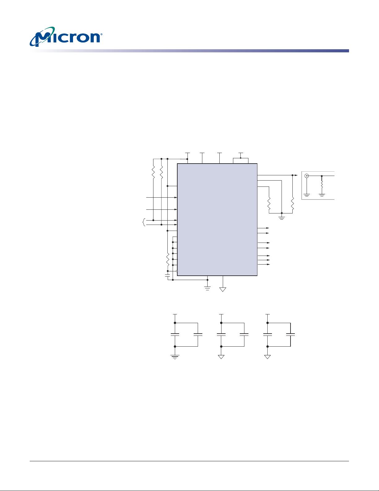
Typical Connections
Figure 4 shows a detailed MT9V125 device configuration. For low-noise operation, the
MT9V125 requires separate analog and digital power supplies. Incoming digital and analog ground conductors can be tied together next to the die.
Power supply voltages V
the pixel array) should be decoupled separately.
The MT9V125 requires a single external voltage supply level.
Figure 4: Typical Configuration (without use of overlay)
AA (the primary analog voltage) and VAAPIX (the main voltage to
Typical Connections
Notes: 1. MT9V125 STANDBY can be connected directly to the customer’s ASIC controller or to DGND,
2. A 1.5KΩ resistor value is recommended, but may be greater for slower (for example,
depending on the controller’s capability.
100Kb) two-wire speed.
3. LVDS_ENABLE must be tied HIGH if LVDS is to be used.
4. Pull down DAC_REF with a 2.8KΩ resistor for 1.0V peak-to-peak video output. For a 1.4V
peak-to-peak video output, change the resistor to 2.4KΩ.
AA and VAAPIX must be tied to the same potential for proper operation.
5. V
PDF: 09005aef829db8a0/Source: 09005aef829dbfdb Micron Technology, Inc., reserves the right to change products or specifications without notice.
MT9V125_LDS_2.fm - Rev. A 4/07 EN
5 ©2007 Micron Technology, Inc. All rights reserved.
Page 6
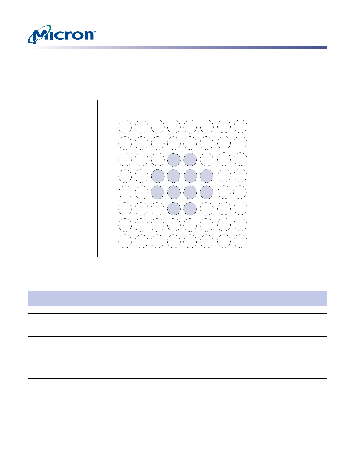
Ball Assignments
Figure 5 shows the location of the balls and their corresponding signals on the MT9V125.
The 12 balls in the middle of the package are unconnected.
Figure 5: 52-Ball iBGA Assignment
1
MT9V125: 1/4-Inch VGA SOC Digital Image Sensor
Ball Assignments
2
4
3
5
6
7 8
A
B
C
D
E
F
G
H
Table 4: Ball Descriptions
LINE_
VDD
DIN7
DIN6
DIN5
DIN3
DIN4
DIN2 DIN0
DIN
DIN1
_CLK
EXT
STANDBY
CLK
RESET
_BAR
SCLK
V
DD
SDATA
OUT4
D
DOUT5
DGND
DGND
S
ADDR
NTSC
_PAL_
SELECT
D
D
RSVD
LVDS_
ENABLE
OUT2
OUT3
OUT0
D
D
OUT1
HORIZ
_FLIP
PEDESTAL
Top View
(Ball Down)
VALID
PIXCLK
GND
D
AGND
VAAPIX
VAA
V
FRAME_
VALID
D
D
DDPLL
OUT
D
_LSB0
OUT
D
_LSB1
OUT6
OUT7
DAC
_NEG
DGND
VDD
LVD S
_POS
LVDS
_NEG
GND
D
VDD
DAC
_POS
VDD
DAC
DAC
_REF
Ball
Assignment Name Type Description
F1 EXTCLK Input
G1 RESET_BAR Input
G3 S
ADDR Input
G4 RSVD Input
G2 SCLK Input
F2 STANDBY Input
G5 HORIZ_FLIP Input
H3 NTSC_PAL_SELECT Input
H5 PEDESTAL Input
PDF: 09005aef829db8a0/Source: 09005aef829dbfdb Micron Technology, Inc., reserves the right to change products or specifications without notice.
MT9V125_LDS_2.fm - Rev. A 4/07 EN
Master clock in sensor.
Active LOW: asynchronous reset.
Two-wire serial interface device ID selection 1:0xBA, 0:0x90.
Must be attached to D
GND. G4
Two-wire serial interface clock.
Multifunctional signal to control device addressing, power-down,
and state functions (covering output enable function).
If “0” at reset: Default horizontal setting.
If “1” at reset: Flips the image readout format in the horizontal
direction.
If “0” at reset: Default NTSC mode.
If “1” at reset: Default PAL mode.
If “0” at reset: Does not add pedestal to composite video output.
If “1” at reset: Adds pedestal to composite video output.
Valid for NTSC only, pull LOW for PAL operation.
6 ©2007 Micron Technology, Inc. All rights reserved.
Page 7

MT9V125: 1/4-Inch VGA SOC Digital Image Sensor
Table 4: Ball Descriptions (continued)
Ball
Assignment Name Type Description
H4 LVDS_ENABLE Input
A2, B1, B2, C1,
IN[7:0] Input
D
C2, D2, E2, D1
E1 DIN_CLK Input
H2 SDATA Output
F7, E7, B3, A3,
OUT[7:0] Output
D
B4, A4, B5, A5
C7 D
D7 D
OUT_LSB0 Output
OUT_LSB1 Output
B7 FRAME_VALID Output
A6 LINE_VALID Output
B6 PIXCLK Output
F8 DAC_POS Output
G7 DAC_NEG Output
H8 DAC_REF Output
B8 LVDS_POS Output
C8 LVDS_NEG Output
F6 A
D8, C3, C6, F3,
GND Supply
GND Supply
D
H7
H6 V
AA Supply
G6 VAAPIX Supply
A1, A8, E8 ,H1 V
G8 V
A7 V
DD Supply
DDDAC Supply
DDPLL Supply
Notes: 1. ALL power pins (VDD/VDDDAC/VDDPLL/VAA/VAAPIX) must be connected to 2.8V
(nominal). Power pins cannot be floated.
2. ALL ground pins (A
floated.
3. Inputs are not tolerant to signal voltages above 3.1V.
4. All unused inputs must be tied to GND or VDD.
AA and VAAPIX must be tied to the same potential for proper operation.
5. V
Active HIGH: Enables the LVDS output port. Must be HIGH if LVDS is
to be used.
External data input port selectable at video encoder input.
IN capture clock. (This clock must be synchronous to EXTCLK.)
D
Two-wire serial interface data I/O.
Pixel data output D
OUT7 (most significant bit [MSB]), DOUT0 (least
significant bit [LSB]). Data output [9:2] in sensor stand-alone mode
Sensor stand-alone mode output 0—typically left unconnected for
normal SOC operation.
Sensor stand-alone mode output 1—typically left unconnected for
normal SOC operation.
Active HIGH: FRAME_VALID (FV); indicates active frame.
Active HIGH: LINE_VALID (LV); indicates active pixel.
Pixel clock output.
Positive video DAC output in differential mode.
Video DAC output in single-ended mode.
Negative video DAC output in differential mode. Tie to GND in
single-ended mode.
External reference resistor for video DAC.
LVDS positive output.
LVDS negative output.
Analog ground.
Digital ground.
Analog power: 2.5–3.1V (2.8V nominal).
Pixel array analog power supply: 2.5–3.1V (2.8V nominal).
Digital power: 2.5–3.1V (2.8V nominal).
DAC power: 2.5–3.1V (2.8V nominal).
LVDS PLL power: 2.5–3.1V (2.8V nominal).
GND/DGND) must be connected to ground. Ground pins cannot be
Ball Assignments
PDF: 09005aef829db8a0/Source: 09005aef829dbfdb Micron Technology, Inc., reserves the right to change products or specifications without notice.
MT9V125_LDS_2.fm - Rev. A 4/07 EN
7 ©2007 Micron Technology, Inc. All rights reserved.
Page 8

Detailed Architecture Overview
Sensor Core
The sensor consists of a pixel array of 695 x 512, an analog readout chain, 10-bit ADC
with programmable gain and black offset, and timing and control, as illustrated in
Figure 6.
Figure 6: Sensor Core Block Diagram
MT9V125: 1/4-Inch VGA SOC Digital Image Sensor
Detailed Architecture Overview
Active Pixel
Sensor (APS)
Array
Analog Processing
Control Register
Timing and Control
ADC
Communication
Bus
to IFP
Clock
Sync
Signals
10-Bit Data
to IFP
There are 649 columns by 498 rows of optically-active pixels that include a pixel boundary around the VGA (640 x 480) image to avoid boundary effects during color interpolation and correction.
The one additional active column and two additional active rows are used to enable horizontally and vertically mirrored readout to start on the same color pixel.
Figure 7 on page 9 illustrates the process of capturing the image. The original scene is
flipped and mirrored by the sensor optics. Sensor readout starts at the lower right hand
corner. The image is presented in true orientation by the output display.
PDF: 09005aef829db8a0/Source: 09005aef829dbfdb Micron Technology, Inc., reserves the right to change products or specifications without notice.
MT9V125_LDS_2.fm - Rev. A 4/07 EN
8 ©2007 Micron Technology, Inc. All rights reserved.
Page 9

Figure 7: Image Capture Example
SCENE
(Front view)
OPTICS
IMAGE CAPTURE
IMAGE RENDERING
Start Readout
Row by Row
IMAGE SENSOR
(Rear view)
Start Rasterization
Process of Ima
g
e
Gatherin
g
and Image Displa
y
DISPLAY
(Front view)
MT9V125: 1/4-Inch VGA SOC Digital Image Sensor
Detailed Architecture Overview
The sensor core uses a paired RGB Bayer color pattern, as shown in Figure 8 on page 10.
Row pairs consist of the following: rows 0, 1, rows 2, 3, rows 4, 5, etc. The even-numbered
row pairs (0/1, 4/5, and so on) in the active array contain green and red color pixels. The
odd-numbered row pairs (2/3, 6/7, and so on) contain blue and green color pixels. The
odd-numbered columns contain green and blue color pixels; even-numbered columns
contain red and green color pixels.
PDF: 09005aef829db8a0/Source: 09005aef829dbfdb Micron Technology, Inc., reserves the right to change products or specifications without notice.
MT9V125_LDS_2.fm - Rev. A 4/07 EN
9 ©2007 Micron Technology, Inc. All rights reserved.
Page 10

MT9V125: 1/4-Inch VGA SOC Digital Image Sensor
Figure 8: Pixel Color Pattern Detail (top right corner)
Column Readout Direction
.
.
.
R
G
R
G
R
G
G
Detailed Architecture Overview
Black Pixels
First Active
Border
Pixel
(42, 13)
Output Data Format
Row
Readout
Direction
...
R
G
G
B
G
B
R
G
R
G
R
G
G
B
G
B
R
G
R
G
R
G
B
B
G
G
G
G
B
G
B
R
G
R
G
The sensor core image data is read out in an interlaced scan order. Progressive readout—
which is not supported by the color pipe—is an option, but is only intended for raw data
output. Valid image data is surrounded by horizontal and vertical blanking, shown in
Figure 9 on page 11.
For NTSC output, the horizontal size is stretched from 640 to 720 pixels. The vertical size
is 243 pixels per field; tom of the image field.
For PAL output, the horizontal size is also stretched from 640 to 720 pixels. The vertical
size is 288 pixels per field—240 image pixels with 24 dark pixels at the top of the image
and 24 dark pixels at the bottom of the image field.
PDF: 09005aef829db8a0/Source: 09005aef829dbfdb Micron Technology, Inc., reserves the right to change products or specifications without notice.
MT9V125_LDS_2.fm - Rev. A 4/07 EN
10 ©2007 Micron Technology, Inc. All rights reserved.
Page 11

MT9V125: 1/4-Inch VGA SOC Digital Image Sensor
P
0,0 P0,1 P0,2
.....................................P
0,n-1 P0,n
P
2,0 P2,1 P2,2
.....................................P
2,n-1 P2,n
00 00 00 .................. 00 00 00
00 00 00 .................. 00 00 00
P
m-2,0 Pm-2,1
.....................................P
m-2,n-1 Pm-2,n
P
m,0 Pm,1
.....................................P
m,n-1 Pm,n
00 00 00 .................. 00 00 00
00 00 00 .................. 00 00 00
00 00 00 .................. 00 00 00
00 00 00 .................. 00 00 00
00 00 00 .................. 00 00 00
00 00 00 .................. 00 00 00
00 00 00 ..................................... 00 00 00
00 00 00 ..................................... 00 00 00
00 00 00 ..................................... 00 00 00
00 00 00 ..................................... 00 00 00
Valid Image Odd Field
Horizontal
Blanking
Vertical Even Blanking
Vertical/Horizontal
Blanking
P
1,0 P1,1 P1,2
.....................................P
1,n-1 P1,n
P
3,0 P3,1 P3,2
.....................................P
3,n-1 P3,n
00 00 00 .................. 00 00 00
00 00 00 .................. 00 00 00
P
m-1,0 Pm-1,1
.....................................P
m-1,n-1 Pm-1,n
P
m+1,0 Pm+1,1
..................................P
m+1,n-1 Pm+1,n
00 00 00 .................. 00 00 00
00 00 00 .................. 00 00 00
00 00 00 .................. 00 00 00
00 00 00 .................. 00 00 00
00 00 00 .................. 00 00 00
00 00 00 .................. 00 00 00
00 00 00 ..................................... 00 00 00
00 00 00 ..................................... 00 00 00
00 00 00 ..................................... 00 00 00
00 00 00 ..................................... 00 00 00
Valid Image Even Field
Horizontal
Blanking
Vertical Odd Blanking
Vertical/Horizontal
Blanking
Figure 9: Spatial Illustration of Image Readout
Detailed Architecture Overview
PDF: 09005aef829db8a0/Source: 09005aef829dbfdb Micron Technology, Inc., reserves the right to change products or specifications without notice.
MT9V125_LDS_2.fm - Rev. A 4/07 EN
11 ©2007 Micron Technology, Inc. All rights reserved.
Page 12

Image Flow Processor
The MT9V125 IFP consists of a color processing pipeline, and a measurement and control logic block (the camera controller). The stream of raw data from the sensor enters
the pipeline and undergoes several transformations. Image stream processing starts
with conditioning the black level and applying a digital gain. The lens shading block
compensates for signal loss caused by the lens.
Next, the data is interpolated to recover missing color components for each pixel. The
resulting interpolated RGB data passes through the current color correction matrix
(CCM) as well as the gamma and saturation corrections, and is formatted for final output.
The measurement and control logic continuously accumulate image brightness and
color statistics. Based on these measurements, the IFP calculates updated values for
exposure time and sensor analog gains that are sent to the sensor core through the control bus.
Black Level Conditioning
The sensor core black level calibration works to maintain black pixel values at a constant
level, independent of analog gain, reference current, voltage settings, and temperature
conditions. If this black level is above zero, it must be reduced before color processing
can begin. The black level subtraction block in the IFP re-maps the black level of the sensor to zero prior to lens shading correction. Following lens shading correction, the black
level addition block provides capability for another black level adjustment. However, for
good contrast, this level should be set to zero.
MT9V125: 1/4-Inch VGA SOC Digital Image Sensor
Detailed Architecture Overview
Digital Gain
Controlled by auto exposure logic, the input digital gain stage amplifies the raw image in
low-light conditions (range: x1–x8).
Test Pattern
A built-in test pattern generator produces a test image stream that can be multiplexed
with the gain stage. The test pattern can be selected through register settings.
Lens Shading Correction
Inexpensive lenses tend to attenuate image intensity near the edges of pixel arrays.
Other factors also cause signal and coloration differences across the image. The net
result of all these factors is known as lens shading. Lens shading correction (LC) compensates for these differences.
Typically, the profile of lens-shading-induced anomalies across the frame is different for
each color component. Therefore, lens shading correction is independently calibrated
for the color channels.
Interpolation and Aperture Correction
A demosaic engine converts the single-color-per-pixel Bayer data from the sensor into
RGB (10-bit per color channel). The demosaic algorithm analyzes neighboring pixels to
generate a best guess for the missing color components. Edge sharpness is preserved as
much as possible.
Aperture correction sharpens the image by an adjustable amount. To avoid amplifying
noise, sharpening can be programmed to phase out as light levels drop.
PDF: 09005aef829db8a0/Source: 09005aef829dbfdb Micron Technology, Inc., reserves the right to change products or specifications without notice.
MT9V125_LDS_2.fm - Rev. A 4/07 EN
12 ©2007 Micron Technology, Inc. All rights reserved.
Page 13

Defect Correction
This device supports 2D defect correction. In 2D defect detection/correction, pixels with
values different from their neighbors by greater than a defined threshold are considered
defects unless near the image boundary. The approach is termed 2D, as pixels on neighboring lines as well as neighboring pixels on the same line are considered in both detection and correction.
Color Correction
To obtain good color rendition and saturation, it is necessary to compensate for the differences between the spectral characteristics of the imager color filter array and the
spectral response of the human eye. This compensation, also known as color separation,
is achieved through linear transformation of the image with a 3 x 3 element color correction matrix. The optimal values for the color correction coefficients depend on the spectra of the incident illumination and can be programmed by the user.
Color Saturation Control
Both color saturation and sharpness enhancement can be set by the user, or adjusted
automatically by tracking the magnitude of the gains used by the auto exposure algorithm.
Automatic White Balance
The MT9V125 has a built-in automatic white balance (AWB) algorithm designed to compensate for the effects of changing scene illumination the color rendition quality. This
sophisticated algorithm consists of three major sub-modules:
• A measurement engine (ME) performing statistical analysis of the image
• A module selecting the optimal color correction matrix
• A module selecting analog color channel gains in the sensor core
While the default algorithm settings are adequate in most situations, the user can reprogram base color correction matrices and limit color channel gains. The AWB does not
attempt to locate the brightest or grayest elements in the image; it performs in-depth
image analysis to differentiate between changes in predominant spectra of illumination
and changes in predominant scene colors. Factory defaults are suitable for most applications, however, a wide range of algorithm parameters can be overwritten by the user
through the serial interface.
MT9V125: 1/4-Inch VGA SOC Digital Image Sensor
Detailed Architecture Overview
Auto Exposure
The auto exposure (AE) algorithm performs automatic adjustments to image brightness
by controlling exposure time and analog gains in the sensor core, as well as digital gain
applied to the image. The algorithm relies on the auto exposure measurement engine
that tracks speed and amplitude changes in the overall luminance of selected windows
in the image.
Backlight compensation is achieved by weighting the luminance in the center of the
image higher than the luminance on the periphery. Other algorithm features include:
fast-fluctuating illumination rejection (time averaging), response-speed control, and
controlled sensitivity to small changes.
While the default settings are adequate in most situations, the user can program target
brightness, measurement window, and other parameters as described above. The auto
exposure algorithm enables compensation for a broad range of illumination intensities.
PDF: 09005aef829db8a0/Source: 09005aef829dbfdb Micron Technology, Inc., reserves the right to change products or specifications without notice.
MT9V125_LDS_2.fm - Rev. A 4/07 EN
13 ©2007 Micron Technology, Inc. All rights reserved.
Page 14

Automatic Flicker Abatement
Flicker occurs when integration time is not an integer multiple of the period of the light
intensity. The automatic flicker abatement block eliminates flicker by limiting exposure
times to integer multiples of the light period.
Gamma Correction
To achieve more life-like quality in an image, the IFP includes gamma correction and
color saturation control. Gamma correction operates on the luminance component of
the image and enables compensation for non-linear dependence of the display device
output versus the driving signal (e.g., monitor brightness versus CRT voltage).
In addition, gamma correction provides range compression, converting 10-bit luminance input to 8-bit output. Pre-gamma image processing generates 10-bit luminance
values ranging from 0 to 896. Piece-wise linear gamma correction utilized in this imager
has ten linear intervals, with end points corresponding to the following input values:
Xi = 0…10 = {0, 16, 32, 64, 128, 256, 384, 512, 640, 768, 896}.
For each input value Xi, the user can program the corresponding output value Yi. Yi values must be monotonically increasing.
NTSC/PAL Encoder
The MT9V125 has an on-chip video encoder to format the data stream for composite
video output in the supported NTSC or PAL formats. The encoder expects CCIR-656
interlaced NTSC or PAL data stream input. By default, the input is taken from the onchip image stream. Input can also be taken from the external DIN port for external
image processing used with the on-chip video encoder and composite output.
MT9V125: 1/4-Inch VGA SOC Digital Image Sensor
Detailed Architecture Overview
PDF: 09005aef829db8a0/Source: 09005aef829dbfdb Micron Technology, Inc., reserves the right to change products or specifications without notice.
MT9V125_LDS_2.fm - Rev. A 4/07 EN
14 ©2007 Micron Technology, Inc. All rights reserved.
Page 15

I/O Timing
t
dout_su
t
dout_ho
EXTCLK
PIXCLK
D
OUT
[7:0]
FRAME_VALID
LINE_VALID
t
pixclk_high
t
extclk_high
t
fvlv_su
t
fvlv_ho
t
extclkr_dout
t
extclkr_fvlv
t
extclk_low
UNDEFINED
Input
Output
Output
Output
t
extclk_period
t
pixclk_period
t
pixclk_low
Digital Output
By default, the MT9V135 launches pixel data, FV, and LV synchronously with the falling
edge of PIXCLK. The expectation is that the user captures data, FV, and LV using the
rising edge of PIXCLK. The timing diagram is shown in Figure 10.
As an option, the polarity of the PIXCLK can be inverted from the default. This is
achieved by programming R155:1[9] to “0.”
Figure 10: Digital Output I/O Timing
MT9V125: 1/4-Inch VGA SOC Digital Image Sensor
Detailed Architecture Overview
Table 5: Digital Output I/O Timing
TA=Ambient = 25°C; VDD = 2.5–3.1V
Signal Parameter Condition Minimum Typical Maximum Unit
t
EXTCLK
PIXCLK
1t
DATA[7:0]
FV/LV
PDF: 09005aef829db8a0/Source: 09005aef829dbfdb Micron Technology, Inc., reserves the right to change products or specifications without notice.
MT9V125_LDS_2.fm - Rev. A 4/07 EN
extclk_high
t
extclk_low
t
extclk_period
f
extclk
max +/- 100 ppm 27 MHz
pixclk_low
t
pixclk_high
t
pixclk_period
t
extclkr_dout
t
dout_su
t
dout_ho
t
extclkr_fvlv
t
fvlv_su
t
fvlv_ho
Notes: 1. PIXCLK may be inverted by programming register R155:1[9] = 0.
15 ©2007 Micron Technology, Inc. All rights reserved.
17 – 20 ns
17 – 20 ns
–37.0– ns
14 – 22 ns
14 – 22 ns
36.7 37 37.4 ns
81418ns
14 18.5 23 ns
14 18.5 23 ns
81418ns
14 18.5 23 ns
14 18.5 23 ns
Page 16

MT9V125: 1/4-Inch VGA SOC Digital Image Sensor
Electrical Specifications
Table 6: Electrical Characteristics and Operating Conditions
TA = Ambient = 25°C; All supplies at 2.8V
Electrical Specifications
Parameter
I/O and core digital voltage (V
LVDS PLL voltage
Video DAC voltage
Analog voltage (V
Pixel supply voltage (V
Leakage current
Imager operating temperature
Functional operating temperature
Storage temperature
1
DD)
AA)
AAPIX)
Notes: 1. VDD, VAA, and VAAPIX must all be at the same potential to avoid excessive current draw.
Care must be taken to avoid excessive noise injection in the analog supplies if all three supplies are tied together.
Condition Minimum Typical Maximum Unit
n/a 2.5 2.8 3.1 V
n/a 2.5 2.8 3.1 V
n/a 2.5 2.8 3.1 V
n/a 2.5 2.8 3.1 V
n/a 2.5 2.8 3.1 V
STANDBY, EXTCLK:
HIGH or LOW
n/a –40 +85 °C
n/a –40 +105 °C
n/a –40 +125 °C
10 µA
Table 7: Video DAC Electrical Characteristics
TA = Ambient = 25°C; All supplies at 2.8V
Parameter Condition Minimum Typ i cal Maximum Unit
Resolution
DNL Single-ended mode
INL Single-ended mode
Output local oad Single-ended mode, output pad (DAC_POS)
Single-ended mode, unused output (DAC_NEG)
Output voltage Single-ended mode, code 000h
Single-ended mode, code 3FFh
Output current Single-ended mode, code 000h
Single-ended mode, code 3FFh
DNL Differential mode
INL Differential mode
Output local load Differential mode per pad
(DAC_POS and DAC_NEG)
Output voltage Differential mode, code 000h, pad dacp
Differential mode, code 000h, pad dacn
Differential mode, code 3FFh, pad dacp
Differential mode, code 3FFH, pad dacn
Output voltage Differential mode, code 000h, pad dacp
Differential mode, code 000h, pad dacn
Differential mode, code 3FFh, pad dacp
Differential mode, code 3FFH, pad dacn
Differential output,
mid level
Supply current Estimate
Differential mode
–10–bits
– 0.8 1.1 bits
– 5.7 8.1 bits
–75–Ω
–0–Ω
–0.02– V
–1.42– V
–0.6–mA
–37.9–mA
– 0.7 1 bits
– 1.4 3 bits
–37.5– Ω
–0.37– V
–1.07– V
–1.07– V
–0.37– V
–0.6–mA
–37.9–mA
–37.9–mA
–0.6–mA
–0.72– V
––55mA
PDF: 09005aef829db8a0/Source: 09005aef829dbfdb Micron Technology, Inc., reserves the right to change products or specifications without notice.
MT9V125_LDS_3.fm - Rev. A 4/07 EN
16 ©2007 Micron Technology, Inc. All rights reserved.
Page 17

MT9V125: 1/4-Inch VGA SOC Digital Image Sensor
Electrical Specifications
Table 8: Digital I/O Parameters
TA = Ambient = 25°C; All supplies at 2.8V
Signal
Type Parameter Definition Condition Minimum Typical Maximum Unit
All
Outputs
Load capacitance
Output signal slew
2.8V, 30pF load – 0.72 – V/ns
1–30pF
2.8V, 5pF load – 1.25 – V/ns
All
Inputs
OH
V
OL
V
OH
I
OL
I
IH
V
IL
V
IN
I
Signal CAP
Output high voltage
Output low voltage
Output high current
Output low current
Input high voltage
Input low voltage
Input leakage current
Input signal capacitance
VDD = 2.8V, VOH = 2.4V 16 – 26.5 mA
DD = 2.8V, VOL = 0.4V 15.9 – 21.3 mA
V
V
DD = 2.8V 1.48 – – V
VDD = 2.8V – – 1.43 V
2.5 2.8 3.1 V
–0.3 – 0.3 V
–2 – 2 µA
–3.5–pF
Power Consumption
Table 9: Power Consumption
TA = Ambient = 25°C; All supplies at 2.8V
Mode
Active mode
Standby
2
Notes: 1. 10pF nominal.
2. (NTSC or PAL) and LVDS should not be operated at the same time.
Sensor
(mW)
Image Flow Processor
(mW)
I/Os
(mW)1
DAC
(mW)
LVDS
(mW)
60 100 10 150 80 400
To ta l
(mW)
0.56
PDF: 09005aef829db8a0/Source: 09005aef829dbfdb Micron Technology, Inc., reserves the right to change products or specifications without notice.
MT9V125_LDS_3.fm - Rev. A 4/07 EN
17 ©2007 Micron Technology, Inc. All rights reserved.
Page 18

MT9V125: 1/4-Inch VGA SOC Digital Image Sensor
Electrical Specifications
NTSC Signal Parameters
Table 10: NTSC Signal Parameters
TA = Ambient = 25°C; All supplies at 2.8V
Parameter Condition Minimum Typical Maximum Unit Notes
Line Frequency
Field Frequency
Sync Rise Time
Sync Fall Time
Sync Width
Sync Level
Burst Level
Sync to Setup
(with pedestal off)
Sync to Burst Start
Front Porch
Burst Width
Black Level
White Level
15730 15735 15740 Hz
59.00 59.94 60.00 Hz
120 164 170 ns
120 167 170 ns
4.60 4.74 4.80 µS
37 39.9 43 IRE 2, 4
37 39.7 43 IRE 2, 4
9.10 9.40 9.40 µS
5.00 5.31 5.60 µS
1.40 1.40 1.60 µS
8.0 8.5 10.0 cycles
6.5 7.5 8.5 IRE 1, 2, 4
90 100 110 IRE 1, 2, 3, 4
Notes: 1. Black and white levels are referenced to the blanking level.
2. NTSC convention standardized by the IRE (1 IRE = 7.14mV).
3. Encoder contrast setting R0x011 = R0x001 = 0.
4. DAC ref = 2.8kΩ, load = 37.5Ω
PDF: 09005aef829db8a0/Source: 09005aef829dbfdb Micron Technology, Inc., reserves the right to change products or specifications without notice.
MT9V125_LDS_3.fm - Rev. A 4/07 EN
18 ©2007 Micron Technology, Inc. All rights reserved.
Page 19

®
MT9V125: 1/4-Inch VGA SOC Digital Image Sensor
Seating
plane
9.000 ±0.075
3.50
3.50
Encapsulant: epoxy
Image sensor die
Lid material: borosilicate glass 0.40 thickness
Optical area
Fuses
0.40
(For reference only)
0.90
5.50 CTR
7.00
5.20
1.845
1.00 TYP
9.000 ±0.075
0.375 ±0.050
0.525 ±0.050
0.125
(For reference only)
C
L
C
L
C
L
C
L
7.00
Substrate material: plastic laminate
Solder ball material: 96.5% Sn, 3% Ag, 0.5% Cu
Maximum rotation of optical area relative to package edges: 1º
0.10 A
A
D
Ball A1 ID
Ball A1
Ball A8
52X Ø0.55
Dimensions apply
to solder balls postreflow. The prereflow diameter is
Ø0.50 on a Ø0.40
SMD ball pad.
1.00 typ
First
clear
pixel
Maximum tilt of optical area relative to package edge : 50 microns
Maximum tilt of optical area relative to top of cover glass: 50 microns
D
3.584 CTR
2.688 CTR
Ø0.15 A B C
Ø0.15 A BC
Optical
center
C
B
Package and Die Dimensions
Figure 11: 52-Ball iBGA Package Outline Drawing
Package and Die Dimensions
Notes: 1. All dimensions in millimeters.
8000 S. Federal Way, P.O. Box 6, Boise, ID 83707-0006, Tel: 208-368-3900
prodmktg@micron.com www.micron.com Customer Comment Line: 800-932-4992
PDF: 09005aef829db8a0/Source: 09005aef829dbfdb Micron Technology, Inc., reserves the right to change products or specifications without notice.
MT9V125_LDS_3.fm - Rev. A 4/07 EN
Micron, the M logo, the Micron logo, and DigitalClarity are trademarks of Micron Technology, Inc.
All other trademarks are the property of their respective owners.
19 ©2007 Micron Technology, Inc. All rights reserved.
 Loading...