

MICRON MT58V512V36DT-7.5, MT58V1MV18DT-6, MT58V1MV18DT-7.5, MT58V1MV18DF-7.5, MT58L512Y36DT-10 Datasheet
...
1
16Mb: 1 Meg x 18, 512K x 32/36 Pipelined, DCD SyncBurst SRAM Micron Technology, Inc., reserves the right to change products or specifications without notice.
MT58L1MY18D_2.p65 – Rev 7/00 ©2000, Micron Technology, Inc.
16Mb: 1 MEG x 18, 512K x 32/36
PIPELINED, DCD SYNCBURST SRAM
ADVANCE
16Mb SYNCBURST
™
SRAM
FEATURES
• Fast clock and OE# access times
• Single +3.3V ±0.165Vor 2.5V ±0.125V power supply
(VDD)
• Separate +3.3V or 2.5V isolated output buffer
supply (VDDQ)
• SNOOZE MODE for reduced-power standby
• Common data inputs and data outputs
• Individual BYTE WRITE control and GLOBAL
WRITE
• Three chip enables for simple depth expansion and
address pipelining
• Clock-controlled and registered addresses, data I/Os
and control signals
• Internally self-timed WRITE cycle
• Burst control (interleaved or linear burst)
• Automatic power-down
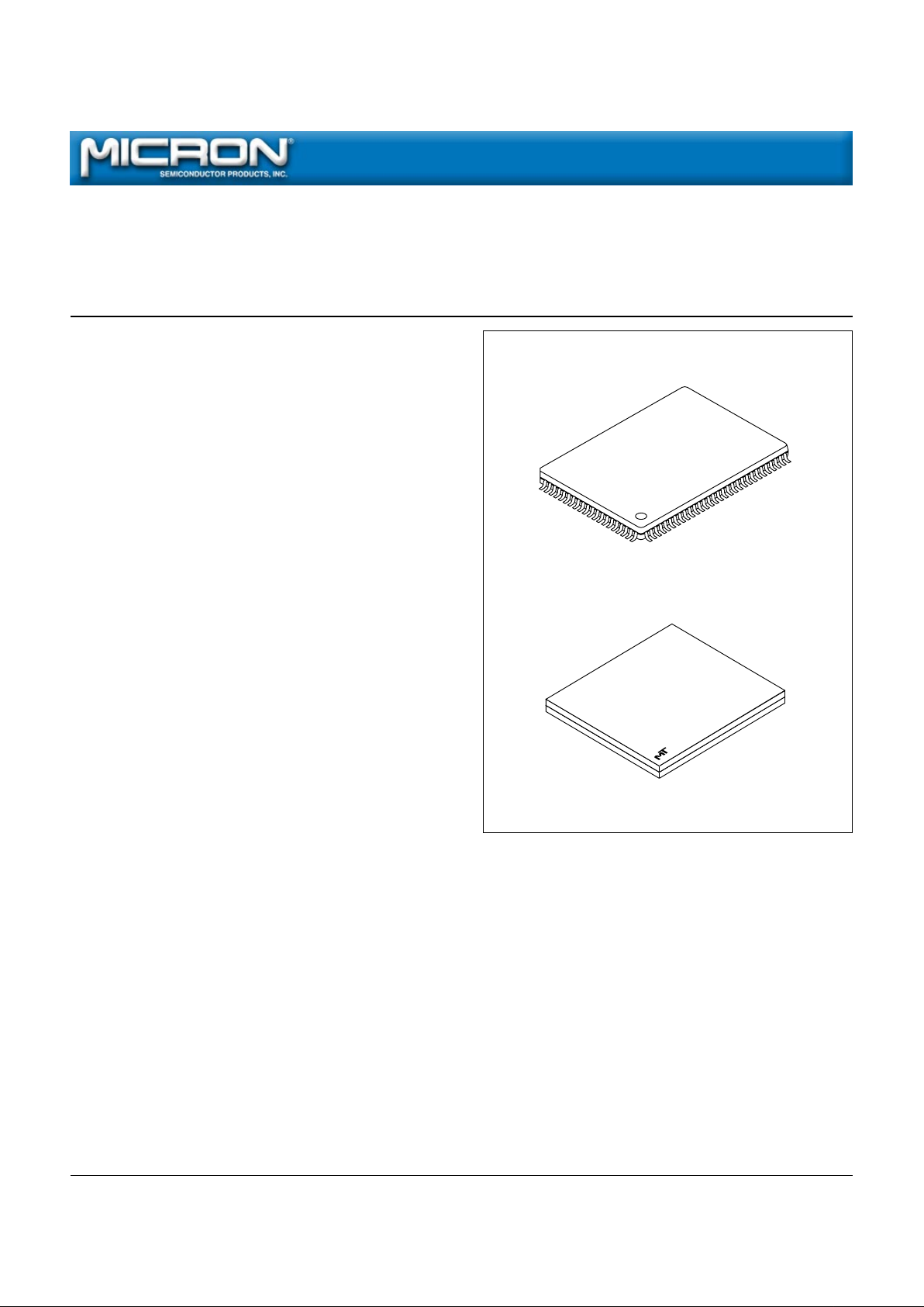
• 100-pin TQFP package
• 165-pin FBGA package
• Low capacitive bus loading
• x18, x32, and x36 versions available
OPTIONS TQFP MARKING*
• Timing (Access/Cycle/MHz)
3.5ns/6ns/166 MHz -6
4.0ns/7.5ns/133 MHz -7.5
5ns/10ns/100 MHz -10
• Configurations
3.3V VDD, 3.3V or 2.5V I/O
1 Meg x 18 MT58L1MY18D
512K x 32 MT58L512Y32D
512K x 36 MT58L512Y36D
2.5V VDD, 2.5V I/O
1 Meg x 18 MT58V1MV18D
512K x 32 MT58V512V32D
512K x 36 MT58V512V36D
• Packages
100-pin TQFP (3-chip enable) T
165-pin FBGA F
• Operating Temperature Range
Commercial (0ºC to +70ºC) None
*See page 34 for FBGA package marking guide.
Part Number Example:
MT58L1MY18DT-7.5
MT58L1MY18D, MT58V1MV18D,
MT58L512Y32D, MT58V512V32D,
MT58L512Y36D, MT58V512V36D
3.3V VDD, 3.3V or 2.5V I/O; 2.5V VDD, 2.5V
I/O, Pipelined, Double-Cycle Deselect
GENERAL DESCRIPTION
The Micron® SyncBurst™ SRAM family employs highspeed, low-power CMOS designs that are fabricated
using an advanced CMOS process.
Micron’s 16Mb SyncBurst SRAMs integrate a 1 Meg x
18, 512K x 32, or 512K x 36 SRAM core with advanced
synchronous peripheral circuitry and a 2-bit burst
counter. All synchronous inputs pass through registers
controlled by a positive-edge-triggered single-clock input (CLK). The synchronous inputs include all addresses,
all data inputs, active LOW chip enable (CE#), two
additional chip enables for easy depth expansion (CE2,
CE2#), burst control inputs (ADSC#, ADSP#, ADV#),
byte write enables (BWx#) and global write (GW#). Note
that CE2# is not available on the T Version.
Asynchronous inputs include the output enable
(OE#), clock (CLK) and snooze enable (ZZ). There is also
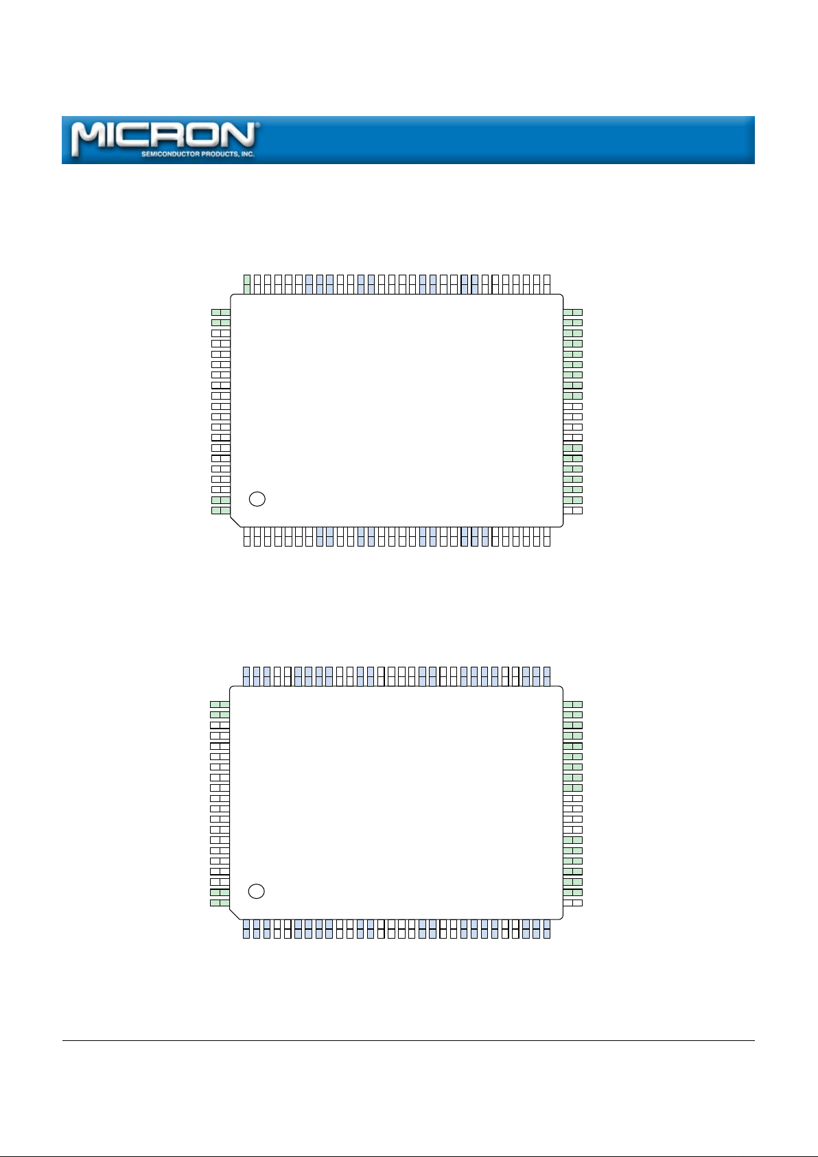
100-Pin TQFP
1
NOTE: 1. JEDEC-standard MS-026 BHA (LQFP).
165-Pin FBGA
(Preliminary Package Data)

2
16Mb: 1 Meg x 18, 512K x 32/36 Pipelined, DCD SyncBurst SRAM Micron Technology, Inc., reserves the right to change products or specifications without notice.
MT58L1MY18D_2.p65 – Rev 7/00 ©2000, Micron Technology, Inc.
16Mb: 1 MEG x 18, 512K x 32/36
PIPELINED, DCD SYNCBURST SRAM
ADVANCE
FUNCTIONAL BLOCK DIAGRAM
1 MEG x 18
SA0, SA1, SAs
ADDRESS
REGISTER
ADV#
CLK
BINARY
COUNTER AND
LOGIC
CLR
Q1
Q0
ADSC#
20
20
18 20
BWb#
BWa#
CE#
BYTE “b”
WRITE REGISTER
BYTE “a”
WRITE REGISTER
ENABLE
REGISTER
SA0'
SA1'
OE#
SENSE
AMPS
1 Meg x 9 x 2
MEMORY
ARRAY
ADSP#
2
SA0-SA1
MODE
CE2
CE2#
GW#
BWE#
PIPELINED
ENABLE
DQs
DQPa
DQPb
2
OUTPUT
REGISTERS
INPUT
REGISTERS
E
BYTE “b”
WRITE DRIVER
BYTE “a”
WRITE DRIVER
OUTPUT
BUFFERS
9
9
9
9
18 18 18 18
18
NOTE: Functional block diagrams illustrate simplified device operation. See truth table, pin descriptions and timing diagrams for
detailed information.
FUNCTIONAL BLOCK DIAGRAM
512K x 32/36
ADDRESS
REGISTER
ADV#
CLK
BINARY
COUNTER
CLR
Q1
Q0
ADSP#
ADSC#
MODE
19
19
17 19
BWd#
BWc#
BWb#
BWa#
BWE#
GW#
CE#
CE2
CE2#
OE#
BYTE “d”
WRITE REGISTER
BYTE “c”
WRITE REGISTER
BYTE “b”
WRITE REGISTER
BYTE “a”
WRITE REGISTER
ENABLE
REGISTER
PIPELINED
ENABLE
DQs
DQPa
DQPb
DQPc
DQPd
4
OUTPUT
REGISTERS
SENSE
AMPS
512K x 8 x 4
(x32)
512K x 9 x 4
(x36)
MEMORY
ARRAY
OUTPUT
BUFFERS
E
BYTE “a”
WRITE DRIVER
BYTE “b”
WRITE DRIVER
BYTE “c”
WRITE DRIVER
BYTE “d”
WRITE DRIVER
INPUT
REGISTERS
SA0, SA1, SAs
SA0'
9
9
9
9
9
9
36 36 36 36
36
9
9
SA1'
SA0-SA1

3
16Mb: 1 Meg x 18, 512K x 32/36 Pipelined, DCD SyncBurst SRAM Micron Technology, Inc., reserves the right to change products or specifications without notice.
MT58L1MY18D_2.p65 – Rev 7/00 ©2000, Micron Technology, Inc.
16Mb: 1 MEG x 18, 512K x 32/36
PIPELINED, DCD SYNCBURST SRAM
ADVANCE
GENERAL DESCRIPTION (continued)
NOTE: 1. No Connect (NC) is used on the x32 version. Parity (DQPx) is used on the x36 version.
TQFP PIN ASSIGNMENT TABLE
PIN # x18 x32/x36
1 NC NC/DQPc
1
2NC DQc
3NC DQc
4VDDQ
5VSS
6NC DQc
7NC DQc
8 DQb DQc
9 DQb DQc
10 VSS
11 VDDQ
12 DQb DQc
13 DQb DQc
14 NC
15 VDD
16 NC
17 VSS
18 DQb DQd
19 DQb DQd
20 VDDQ
21 VSS
22 DQb DQd
23 DQb DQd
24 DQPb DQd
25 NC DQd
PIN # x18 x32/x36 PIN # x18 x32/x36 PIN # x18 x32/x36
51 NC NC/DQPa
1
52 NC DQa
53 NC DQa
54 VDDQ
55 VSS
56 NC DQa
57 NC DQa
58 DQa
59 DQa
60 VSS
61 VDDQ
62 DQa
63 DQa
64 ZZ
65 VDD
66 NC
67 VSS
68 DQa DQb
69 DQa DQb
70 VDDQ
71 VSS
72 DQa DQb
73 DQa DQb
74 DQPa DQb
75 NC DQb
26 VSS
27 VDDQ
28 NC DQd
29 NC DQd
30 NC NC/DQPd
1
31 MODE (LBO#)
32 SA
33 SA
34 SA
35 SA
36 SA1
37 SA0
38 DNU
39 DNU
40 VSS
41 VDD
42 SA
43 SA
44 SA
45 SA
46 SA
47 SA
48 SA
49 SA
50 SA
a burst mode input (MODE) that selects between interleaved and linear burst modes. The data-out (Q), enabled by OE#, is also asynchronous. WRITE cycles can be
from one to two bytes wide (x18) or from one to four
bytes wide (x32/x36), as controlled by the write control
inputs.
Burst operation can be initiated with either address
status processor (ADSP#) or address status controller
(ADSC#) inputs. Subsequent burst addresses can be internally generated as controlled by the burst advance
input (ADV#).
Address and write control are registered on-chip to
simplify WRITE cycles. This allows self-timed WRITE
cycles. Individual byte enables allow individual bytes to
be written. During WRITE cycles on the x18 device,
BWa# controls DQas and DQPa; BWb# controls DQbs
and DQPb. During WRITE cycles on the x32 and x36
devices, BWa# controls DQas and DQPa; BWb# controls
DQbs and DQPb; BWc# controls DQcs and DQPc; BWd#
controls DQds and DQPd. GW# LOW causes all bytes to
be written. Parity bits are only available on the x18 and
x36 versions.
This device incorporates an additional pipelined
enable register which delays turning off the output
buffer an additional cycle when a deselect is executed.
This feature allows depth expansion without penalizing
system performance.
Micron’s 16Mb SyncBurst SRAMs operate from a
+3.3V or +2.5V power supply, and all inputs and outputs
are TTL-compatible. Users can implement either a 3.3V
or 2.5V I/O for the +3.3V VDD or a 2.5V I/O for the +2.5V
VDD. The device is ideally suited for Pentium® and
PowerPC pipelined systems and systems that benefit
from a very wide, high-speed data bus. The device is also
ideal in generic 16-, 18-, 32-, 36-, 64-, and 72-bit-wide
applications.
Please refer to the Micron Web site
(www.micronsemi.com/en/products/sram/) for the latest data sheet.
76 VSS
77 VDDQ
78 NC DQb
79 NC DQb
80 SA NC/DQPb
1
81 SA
82 SA
83 ADV#
84 ADSP#
85 ADSC#
86 OE# (G#)
87 BWE#
88 GW#
89 CLK
90 VSS
91 VDD
92 CE2#
93 BWa#
94 BWb#
95 NC BWc#
96 NC BWd#
97 CE2
98 CE#
99 SA
100 SA
4
16Mb: 1 Meg x 18, 512K x 32/36 Pipelined, DCD SyncBurst SRAM Micron Technology, Inc., reserves the right to change products or specifications without notice.
MT58L1MY18D_2.p65 – Rev 7/00 ©2000, Micron Technology, Inc.
16Mb: 1 MEG x 18, 512K x 32/36
PIPELINED, DCD SYNCBURST SRAM
ADVANCE
PIN ASSIGNMENT (TOP VIEW)
100-PIN TQFP
NOTE: 1. No Connect (NC) is used on the x32 version. Parity (DQPx) is used on the x36 version.
SA
SA
ADV#
ADSP#
ADSC#
OE# (G#)
BWE#
GW#
CLK
V
SS
V
DD
CE2#
BWa#
BWb#
NC
NC
CE2
CE#
SA
SA
81
82
83
84
85
86
87
88
89
90
91
92
93
94
95
96
97
98
99
100
50
49
48
47
46
45
44
43
42
41
40
39
38
37
36
35
34
33
32
31
80 79 78 77 76 75 74 73 72 71 70 69 68 67 66 65 64 63 62 61 60 59 58 57 56 55 54 53 52 51
1 2 3 4 5 6 7 8 9 10 11 12 13 14 15 16 17 18 19 20 21 22 23 24 25 26 27 28 29 30
SANCNC
V
DD
Q
V
SS
NC
DQPa
DQa
DQa
VSSV
DD
Q
DQa
DQa
V
SS
NC
VDDZZ
DQa
DQa
V
DD
Q
V
SS
DQa
DQaNCNC
VSSV
DD
Q
NCNCNC
SA
SA
SA
SA
SA
SA
SA
SA
SA
V
DD
V
SS
DNU
DNU
SA0
SA1
SA
SA
SA
SA
MODE (LBO#)
NCNCNC
V
DD
Q
V
SS
NC
NC
DQb
DQb
V
SS
V
DD
Q
DQb
DQb
NC
V
DD
NC
V
SS
DQb
DQb
V
DD
Q
V
SS
DQb
DQb
DQPb
NC
V
SS
V
DD
Q
NCNCNC
x18
SA
SA
ADV#
ADSP#
ADSC#
OE# (G#)
BWE#
GW#
CLK
V
SS
V
DD
CE2#
BWa#
BWb#
BWc#
BWd#
CE2
CE#
SA
SA
81
82
83
84
85
86
87
88
89
90
91
92
93
94
95
96
97
98
99
100
50
49
48
47
46
45
44
43
42
41
40
39
38
37
36
35
34
33
32
31
80 79 78 77 76 75 74 73 72 71 70 69 68 67 66 65 64 63 62 61 60 59 58 57 56 55 54 53 52 51
1 2 3 4 5 6 7 8 9 10 11 12 13 14 15 16 17 18 19 20 21 22 23 24 25 26 27 28 29 30
NC/DQPb1DQb
DQb
V
DD
Q
V
SS
DQb
DQb
DQb
DQb
VSSV
DD
Q
DQb
DQb
V
SS
NC
VDDZZ
DQa
DQa
V
DD
Q
V
SS
DQa
DQa
DQa
DQa
VSSV
DD
Q
DQa
DQa
NC/DQPa
1
SA
SA
SA
SA
SA
SA
SA
SA
SA
V
DD
V
SS
DNU
DNU
SA0
SA1
SA
SA
SA
SA
MODE (LBO#)
NC/DQPc
1
DQc
DQc
V
DD
Q
V
SS
DQc
DQc
DQc
DQc
V
SS
V
DD
Q
DQc
DQc
NC
V
DD
NC
V
SS
DQd
DQd
V
DD
Q
V
SS
DQd
DQd
DQd
DQd
V
SS
V
DD
Q
DQd
DQd
NC/DQPd
1
x32/x36

5
16Mb: 1 Meg x 18, 512K x 32/36 Pipelined, DCD SyncBurst SRAM Micron Technology, Inc., reserves the right to change products or specifications without notice.
MT58L1MY18D_2.p65 – Rev 7/00 ©2000, Micron Technology, Inc.
16Mb: 1 MEG x 18, 512K x 32/36
PIPELINED, DCD SYNCBURST SRAM
ADVANCE
TQFP PIN DESCRIPTIONS
x18 x32/x36 SYMBOL TYPE DESCRIPTION
37 37 S A 0 Input Synchronous Address Inputs: These inputs are registered and must
36 36 SA1 meet the setup and hold times around the rising edge of CLK.
32-35, 42-50, 32-35, 42-50, SA
80-82, 99, 81, 82, 99,
100 100
93 93 BWa# Input Synchronous Byte Write Enables: These active LOW inputs allow
94 94 BWb# individual bytes to be written and must meet the setup and hold
– 95 BWc# times around the rising edge of CLK. A byte write enable is LOW
– 96 BWd# for a WRITE cycle and HIGH for a READ cycle. For the x18 version,
BWa# controls DQa pins and DQPa; BWb# controls DQb pins and
DQPb. For the x32 and x36 versions, BWa# controls DQa pins and
DQPa; BWb# controls DQb pins and DQPb; BWc# controls DQc pins
and DQPc; BWd# controls DQd pins and DQPd. Parity is only
available on the x18 and x36 versions.
87 87 BWE# Input Byte Write Enable: This active LOW input permits BYTE WRITE
operations and must meet the setup and hold times around the
rising edge of CLK.
88 8 8 GW# Input Global Write: This active LOW input allows a full 18-, 32-, or 36-bit
WRITE to occur independent of the BWE# and BWx# lines and
must meet the setup and hold times around the rising edge of
CLK.
89 8 9 CLK Input Clock: This signal registers the address, data, chip enable, byte
write enables and burst control inputs on its rising edge. All
synchronous inputs must meet setup and hold times around the
clock’s rising edge.
98 98 CE# Input Synchronous Chip Enable: This active LOW input is used to enable
the device and conditions the internal use of ADSP#. CE# is
sampled only when a new external address is loaded.
92 92 CE2# Input Synchronous Chip Enable: This active LOW input is used to enable
the device and is sampled only when a new external address is
loaded.
64 64 ZZ Input Snooze Enable: This active HIGH, asynchronous input causes the
device to enter a low-power standby mode in which all data in the
memory array is retained. When ZZ is active, all other inputs are
ignored.
This pin has an internal pull-down and can be floating.
97 97 CE2 Input Synchronous Chip Enable: This active HIGH input is used to enable
the device and is sampled only when a new external address is
loaded.
86 86 OE# Input Output Enable: This active LOW, asynchronous input enables the
(G#) data I/O output drivers.
G# is the JEDEC-standard term for OE#.
83 83 ADV# Input Synchronous Address Advance: This active LOW input is used to
advance the internal burst counter, controlling burst access after
the external address is loaded. A HIGH on this pin effectively
causes wait states to be generated (no address advance). To ensure
use of correct address during a WRITE cycle, ADV# must be HIGH at
the rising edge of the first clock after an ADSP# cycle is initiated.
(continued on next page)

6
16Mb: 1 Meg x 18, 512K x 32/36 Pipelined, DCD SyncBurst SRAM Micron Technology, Inc., reserves the right to change products or specifications without notice.
MT58L1MY18D_2.p65 – Rev 7/00 ©2000, Micron Technology, Inc.
16Mb: 1 MEG x 18, 512K x 32/36
PIPELINED, DCD SYNCBURST SRAM
ADVANCE
TQFP PIN DESCRIPTIONS (continued)
x18 x32/x36 SYMBOL TYPE DESCRIPTION
84 84 ADSP# Input Synchronous Address Status Processor: This active LOW input
interrupts any ongoing burst, causing a new external address to be
registered. A READ is performed using the new address,
independent of the byte write enables and ADSC#, but dependent
upon CE#, CE2, and CE2#. ADSP# is ignored if CE# is HIGH. Powerdown state is entered if CE2 is LOW or CE2# is HIGH.
85 85 ADSC# Input Synchronous Address Status Controller: This active LOW input
interrupts any ongoing burst, causing a new external address to be
registered. A READ or WRITE is performed using the new address if
CE# is LOW. ADSC# is also used to place the chip into power-down
state when CE# is HIGH.
31 31 MODE Input Mode: This input selects the burst sequence. A LOW on this pin
(LBO#) selects “linear burst.” NC or HIGH on this pin selects “interleaved
burst.” Do not alter input state while device is operating.
LBO# is
the JEDEC-standard term for MODE.
(a) 58, 59, (a) 52, 53, DQa Input/ SRAM Data I/Os: For the x18 version, Byte “a” is
associated with
62, 63, 68, 69, 56-59, 62, 63 Output DQa pins; Byte “b” is
associated with
DQb pins. For the x32 and
72, 73 x36 versions, Byte “a” is
associated with
DQa pins; Byte “b” is
(b) 8, 9, 12, (b) 68, 69 DQb
associated with
DQb pins; Byte “c” is
associated with
DQc pins;
13, 18, 19, 22, 72-75, 78, 79 Byte “d” is
associated with
DQd pins. Input data must meet setup
23 and hold times around the rising edge of CLK.
(c) 2, 3, 6-9, DQc
12, 13
(d) 18, 19, DQd
22-25, 28, 29
74 51 NC/DQPa NC/ No Connect/Parity Data I/Os: On the x32 version, these pins are No
24 80 NC/DQPb I/O Connect (NC). On the x18 version, Byte “a” parity is DQPa; Byte
– 1 NC/DQPc “b” parity is DQPb. On the x36 version, Byte “a” parity is DQPa;
– 30 NC/DQPd Byte “b” parity is DQPb; Byte “c” parity is DQPc; Byte “d” parity is
DQPd.
15, 41, 65, 15, 41, 65, VDD Supply Power Supply: See DC Electrical Characteristics and Operating
91 91 Conditions for range.
4, 11, 20, 27, 4, 11, 20, 27, VDDQ Supply Isolated Output Buffer Supply: See DC Electrical Characteristics and
54, 61, 70, 77 54, 61, 70, 77 Operating Conditions for range.
5, 10, 17, 21, 5, 10, 17, 21, VSS Supply Ground: GND.
26, 40, 55, 60, 26, 40, 55, 60,
67, 71, 76, 90 67, 71, 76, 90
38, 39 38, 39 DNU – Do Not Use: These signals may either be unconnected or wired to
GND to improve package heat dissipation.
1-3, 6, 7, 14 14, 16, 66 NC – No Connect: These signals are not internally connected and may be
16, 25, 28-30, connected to ground to improve package heat dissipation.
51-53, 56, 57,
66, 75, 78, 79,
95, 96
NA NA NF – No Function: These pins are internally connected to the die and
have the capacitance of an input pin. It is allowable to leave these
pins unconnected or driven by signals.
7
16Mb: 1 Meg x 18, 512K x 32/36 Pipelined, DCD SyncBurst SRAM Micron Technology, Inc., reserves the right to change products or specifications without notice.
MT58L1MY18D_2.p65 – Rev 7/00 ©2000, Micron Technology, Inc.
16Mb: 1 MEG x 18, 512K x 32/36
PIPELINED, DCD SYNCBURST SRAM
ADVANCE
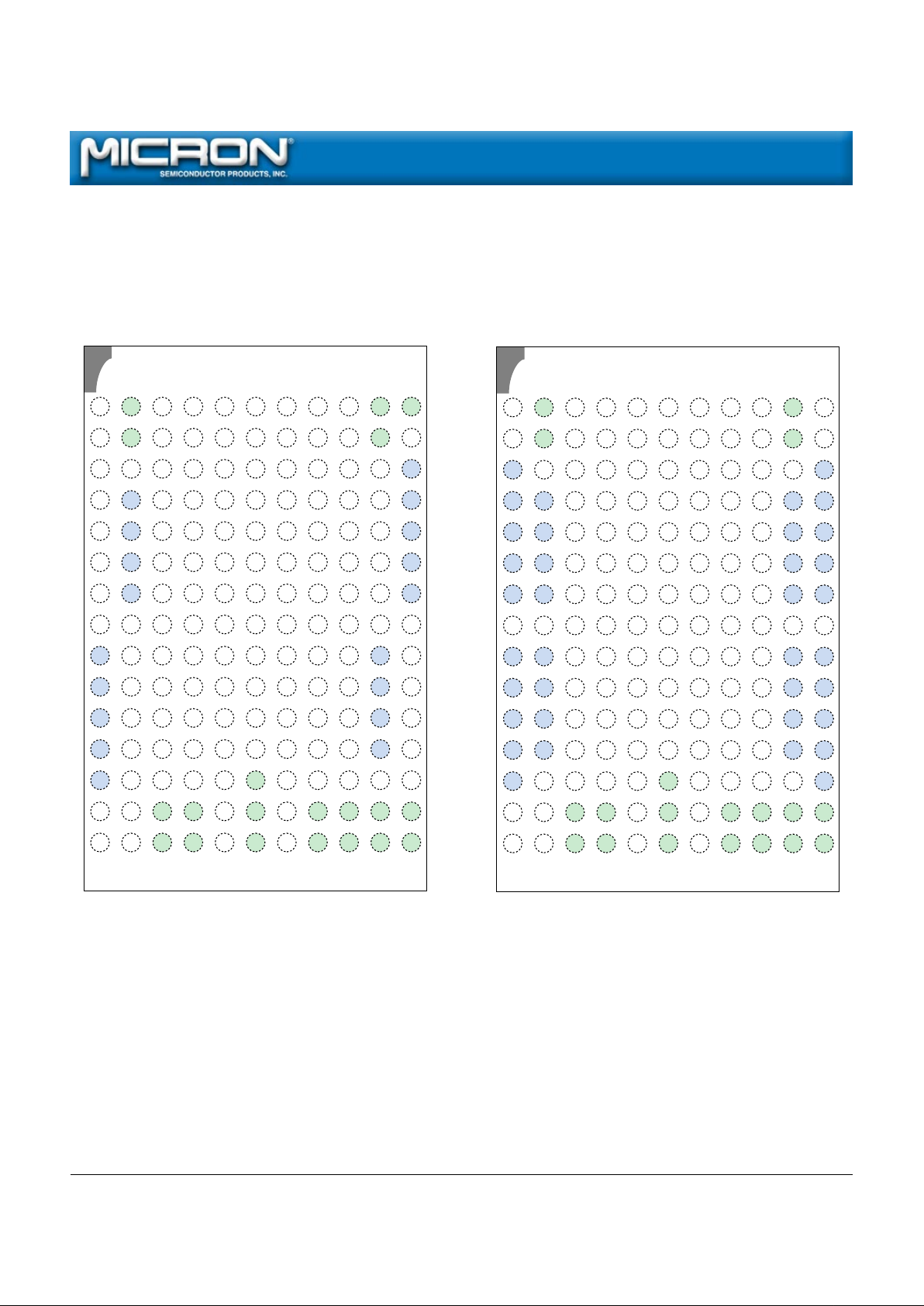
PIN LAYOUT (TOP VIEW)
165-PIN FBGA
A
B
C
D
E
F
G
H
J
K
L
M
N
P
R
A
B
C
D
E
F
G
H
J
K
L
M
N
P
R
2
CE#
CE2
V
DD
Q
V
DD
Q
V
DD
Q
V
DD
Q
V
DD
Q
NC
V
DD
Q
V
DD
Q
V
DD
Q
V
DD
Q
V
DD
Q
SA
SA
SA
SA
NC
DQb
DQb
DQb
DQb
V
SS
NC
NC
NC
NC
NC
NC
NC
NC
NC
NC
NC
NC
NC
NC
V
DD
DQb
DQb
DQb
DQb
DQPb
NC
MODE
(LBO#)
BWb#
NC
V
SS
V
DD
V
DD
V
DD
V
DD
V
DD
V
DD
V
DD
V
DD
V
DD
V
SS
SA
SA
NC
BWa#
V
SS
V
SS
V
SS
V
SS
V
SS
V
SS
V
SS
V
SS
V
SS
V
SS
NC
DNU
DNU
CE2#
CLK
V
SS
V
SS
V
SS
V
SS
V
SS
V
SS
V
SS
V
SS
V
SS
V
SS
SA
SA1
SA0
BWE#
GW#
V
SS
V
SS
V
SS
V
SS
V
SS
V
SS
V
SS
V
SS
V
SS
V
SS
V
SS
DNU
DNU
ADSC#
OE# (G#)
V
SS
V
DD
V
DD
V
DD
V
DD
V
DD
V
DD
V
DD
V
DD
V
DD
V
SS
SA
SA
ADV#
ADSP#
V
DD
Q
V
DD
Q
V
DD
Q
V
DD
Q
V
DD
Q
NC
V
DD
Q
V
DD
Q
V
DD
Q
V
DD
Q
V
DD
Q
SA
SA
SA
SA
NC
NC
NC
NC
NC
NC
DQa
DQa
DQa
DQa
NC
SA
SA
SA
NC
DQPa
DQa
DQa
DQa
DQa
ZZ
NC
NC
NC
NC
NC
SA
SA
TOP VIEW
3456789
10 11
1
A
B
C
D
E
F
G
H
J
K
L
M
N
P
R
A
B
C
D
E
F
G
H
J
K
L
M
N
P
R
2
CE#
CE2
V
DD
Q
V
DD
Q
V
DD
Q
V
DD
Q
V
DD
Q
NC
V
DD
Q
V
DD
Q
V
DD
Q
V
DD
Q
V
DD
Q
SA
SA
SA
SA
NC
DQc
DQc
DQc
DQc
V
SS
DQd
DQd
DQd
DQd
NC
NC
NC
NC
NC
NC/DQPc
DQc
DQc
DQc
DQc
V
DD
DQd
DQd
DQd
DQd
NC/DQPd
NC
MODE
(LBO#)
BWc#
BWd#
V
SS
V
DD
V
DD
V
DD
V
DD
V
DD
V
DD
V
DD
V
DD
V
DD
V
SS
SA
SA
BWb#
BWa#
V
SS
V
SS
V
SS
V
SS
V
SS
V
SS
V
SS
V
SS
V
SS
V
SS
NC
DNU
DNU
CE2#
CLK
V
SS
V
SS
V
SS
V
SS
V
SS
V
SS
V
SS
V
SS
V
SS
V
SS
SA
SA1
SA0
BWE#
GW#
V
SS
V
SS
V
SS
V
SS
V
SS
V
SS
V
SS
V
SS
V
SS
V
SS
V
SS
DNU
DNU
ADSC#
OE# (G#)
V
SS
V
DD
V
DD
V
DD
V
DD
V
DD
V
DD
V
DD
V
DD
V
DD
V
SS
SA
SA
ADV#
ADSP#
V
DD
Q
V
DD
Q
V
DD
Q
V
DD
Q
V
DD
Q
NC
V
DD
Q
V
DD
Q
V
DD
Q
V
DD
Q
V
DD
Q
SA
SA
SA
SA
NC
DQb
DQb
DQb
DQb
NC
DQa
DQa
DQa
DQa
NC
SA
SA
NC
NC
NC/DQPb
DQb
DQb
DQb
DQb
ZZ
DQa
DQa
DQa
DQa
NC/DQPa
SA
SA
TOP VIEW
3456789
10 11
1
x18
x32/x36
*No Connect (NC) is used on the x32 version. Parity (DQPx) is used on the x36 version.

8
16Mb: 1 Meg x 18, 512K x 32/36 Pipelined, DCD SyncBurst SRAM Micron Technology, Inc., reserves the right to change products or specifications without notice.
MT58L1MY18D_2.p65 – Rev 7/00 ©2000, Micron Technology, Inc.
16Mb: 1 MEG x 18, 512K x 32/36
PIPELINED, DCD SYNCBURST SRAM
ADVANCE
FBGA PIN DESCRIPTIONS
x18 x32/x36 SYMBOL TYPE DESCRIPTION
6R 6R SA0 Input Synchronous Address Inputs: These inputs are registered and must
6P 6P SA1 meet the setup and hold times around the rising edge of CLK.
2A, 2B, 3P, 2A, 2B, 3P, SA
3R, 4P, 4R, 6N, 3R, 4P, 4R, 6N,
8P, 8R, 9P, 9R, 8P, 8R, 9P,
10A, 10B, 10P, 9R, 10A, 10B,
10R, 11A, 11P, 10P, 10R, 11P,
11R 11R
5B 5B BWa# Input Synchronous Byte Write Enables: These active LOW inputs allow
4A 5A BWb# individual bytes to be written and must meet the setup and hold
– 4A B Wc# times around the rising edge of CLK. A byte write enable is LOW
– 4B BWd# for a WRITE cycle and HIGH for a READ cycle. For the x18 version,
BWa# controls DQa’s and DQPa; BWb# controls DQb’s and DQPb.
For the x32 and x36 versions, BWa# controls DQa’s and DQPa; BWb#
controls DQb’s and DQPb; BWc# controls DQc’s and DQPc; BWd#
controls DQd’s and DQPd. Parity is only available on the x18 and
x36 versions.
7A 7A BWE# Input Byte Write Enable: This active LOW input permits BYTE WRITE
operations and must meet the setup and hold times around the
rising edge of CLK.
7B 7B GW# Input Global Write: This active LOW input allows a full 18-, 32- or 36-bit
WRITE to occur independent of the BWE# and BWx# lines and must
meet the setup and hold times around the rising edge of CLK.
6B 6B CLK Input Clock: This signal registers the address, data, chip enable, byte write
enables, and burst control inputs on its rising edge. All synchronous
inputs must meet setup and hold times around the clock’s rising
edge.
3A 3A CE# Input Synchronous Chip Enable: This active LOW input is used to enable
the device and conditions the internal use of ADSP#. CE# is sampled
only when a new external address is loaded.
6A 6A CE2# Input Synchronous Chip Enable: This active LOW input is used to enable
the device and is sampled only when a new external address is
loaded.
11H 11H ZZ Input Snooze Enable: This active HIGH, asynchronous input causes the
device to enter a low-power standby mode in which all data in the
memory array is retained. When ZZ is active, all other inputs are
ignored.
3B 3B CE2 Input Synchronous Chip Enable: This active HIGH input is used to enable
the device and is sampled only when a new external address is
loaded.
8B 8B OE#(G#) Input Output Enable: This active LOW, asynchronous input enables the
data I/O output drivers.
(continued on next page)
9
16Mb: 1 Meg x 18, 512K x 32/36 Pipelined, DCD SyncBurst SRAM Micron Technology, Inc., reserves the right to change products or specifications without notice.
MT58L1MY18D_2.p65 – Rev 7/00 ©2000, Micron Technology, Inc.
16Mb: 1 MEG x 18, 512K x 32/36
PIPELINED, DCD SYNCBURST SRAM
ADVANCE
FBGA PIN DESCRIPTIONS (continued)
x18 x32/x36 SYMBOL TYPE DESCRIPTION
9A 9A ADV# Input Synchronous Address Advance: This active LOW input is used to
advance the internal burst counter, controlling burst access after the
external address is loaded. A HIGH on ADV# effectively causes wait
states to be generated (no address advance). To ensure use of
correct address during a WRITE cycle, ADV# must be HIGH at the
rising edge of the first clock after an ADSP# cycle is initiated.
9B 9B ADSP# Input Synchronous Address Status Processor: This active LOW input
interrupts any ongoing burst, causing a new external address to be
registered. A READ is performed using the new address,
independent of the byte write enables and ADSC#, but dependent
upon CE#, CE2, and CE2#. ADSP# is ignored if CE# is HIGH. Powerdown state is entered if CE2 is LOW or CE2# is HIGH.
8A 8A ADSC# Input Synchronous Address Status Controller: This active LOW input
interrupts any ongoing burst, causing a new external address to be
registered. A READ or WRITE is performed using the new address if
CE# is LOW. ADSC# is also used to place the chip into power-down
state when CE# is HIGH.
1R 1R MODE Input Mode: This input selects the burst sequence. A LOW on this
(LB0#) input selects “linear burst.” NC or HIGH on this input selects
“interleaved burst.” Do not alter input state while device is
operating.
(a) 10J, 10K, (a) 10J, 10K, DQa Input/ SRAM Data I/Os: For the x18 version, Byte “a” is associated DQas;
10L, 10M, 11D, 10L, 10M, 11J, Output Byte “b” is associated with DQbs. For the x32 and x36 versions,
11E, 11F, 11G 11K, 11L, 11M Byte “a” is associated with DQas; Byte “b” is associated with DQbs;
(b) 1J, 1K, (b) 10D, 10E, DQb Byte “c” is associated with DQcs; Byte “d” is associated with DQds.
1L, 1M, 2D, 10F, 10G, 11D, Input data must meet setup and hold times around the rising edge
2E, 2F, 2G 11E, 11F, 11G of CLK.
(c) 1D, 1E, DQc
1F, 1G, 2D,
2E, 2F, 2G
(d) 1J, 1K, 1L, D Qd
1M, 2J, 2K,
2L, 2M
11C 11N NC/DQPa NC / No Connect/Parity Data I/Os: On the x32 version, these are No
1N 11C NC/DQPb I/O Connect (NC). On the x18 version, Byte “a” parity is DQPa; Byte “b”
– 1C NC/DQPc parity is DQPb. On the x36 version, Byte “a” parity is DQPa; Byte
– 1N NC/DQPd “b” parity is DQPb; Byte “c” parity is DQPc; Byte “d” parity is DQPd.
1H, 4D, 4E, 4F, 1H, 4D, 4E, 4F, V
DD
Supply Power Supply: See DC Electrical Characteristics and Operating
4G, 4H, 4J, 4G, 4H, 4J, Conditions for range.
4K, 4L, 4M, 4K, 4L, 4M,
8D, 8E, 8F, 8D, 8E, 8F,
8G, 8H, 8J, 8G, 8H, 8J,
8K, 8L, 8M 8K, 8L, 8M
(continued on next page)

10
16Mb: 1 Meg x 18, 512K x 32/36 Pipelined, DCD SyncBurst SRAM Micron Technology, Inc., reserves the right to change products or specifications without notice.
MT58L1MY18D_2.p65 – Rev 7/00 ©2000, Micron Technology, Inc.
16Mb: 1 MEG x 18, 512K x 32/36
PIPELINED, DCD SYNCBURST SRAM
ADVANCE
FBGA PIN DESCRIPTIONS (continued)
x18 x32/x36 SYMBOL TYPE DESCRIPTION
3C, 3D, 3E, 3C, 3D, 3E, VDDQ Supply Isolated Output Buffer Supply: See DC Electrical Characteristics and
3F, 3G, 3J, 3F, 3G, 3J, Operating Conditions for range.
3K, 3L, 3M, 3K, 3L, 3M,
3N, 9C, 9D, 3N, 9C, 9D,
9E, 9F, 9G, 9E, 9F, 9G,
9J, 9K, 9L, 9J, 9K, 9L,
9M, 9N 9M, 9N
2H, 4C, 4N, 5C, 2H, 4C, 4N, 5C, V
SS
Supply Ground: GND.
5D, 5E 5F, 5D, 5E 5F,
5G, 5H, 5J, 5G, 5H, 5J,
5K, 5L, 5M, 5K, 5L, 5M,
6C, 6D, 6E, 6F, 6C, 6D, 6E, 6F,
6G, 6H, 6J, 6G, 6H, 6J,
6K, 6L, 6M, 6K, 6L, 6M,
7C, 7D, 7E, 7C, 7D, 7E,
7F, 7G, 7H, 7F, 7G, 7H,
7J, 7K, 7L, 7J, 7K, 7L,
7M, 7N, 8C, 8N 7M, 7N, 8C, 8N
5P, 5R, 7P, 7R 5P, 5R, 7P, 7R DNU – Do Not Use: These signals may either be unconnected or wired to
GND to improve package heat dissipation.
1A, 1B, 1C, 1A, 1B, 1P, NC – No Connect: These signals are not internally connected and
1D, 1E, 1F, 2C, 2N, 2P, may be connected to ground to improve package heat
1G, 1P, 2C, 2R, 3H, 5N, dissipation.
2J, 2K, 2L, 9H, 10C, 10H,
2M, 2N, 2P, 10N, 11A, 11B
2R, 3H, 4B,
5A, 5N, 9H,
10C, 10D, 10E,
10F, 10G, 10H,
10N, 11B, 11J,
11K, 11L,
11M, 11N
11
16Mb: 1 Meg x 18, 512K x 32/36 Pipelined, DCD SyncBurst SRAM Micron Technology, Inc., reserves the right to change products or specifications without notice.
MT58L1MY18D_2.p65 – Rev 7/00 ©2000, Micron Technology, Inc.
16Mb: 1 MEG x 18, 512K x 32/36
PIPELINED, DCD SYNCBURST SRAM
ADVANCE
INTERLEAVED BURST ADDRESS TABLE (MODE = NC OR HIGH)
FIRST ADDRESS (EXTERNAL) SECOND ADDRESS (INTERNAL) THIRD ADDRESS (INTERNAL) FOURTH ADDRESS (INTERNAL)
X...X00 X...X01 X...X10 X...X11
X...X01 X...X00 X...X11 X...X10
X...X10 X...X11 X...X00 X...X01
X...X11 X...X10 X...X01 X...X00
LINEAR BURST ADDRESS TABLE (MODE = LOW)
FIRST ADDRESS (EXTERNAL) SECOND ADDRESS (INTERNAL) THIRD ADDRESS (INTERNAL) FOURTH ADDRESS (INTERNAL)
X...X00 X...X01 X...X10 X...X11
X...X01 X...X10 X...X11 X...X00
X...X10 X...X11 X...X00 X...X01
X...X11 X...X00 X...X01 X...X10
PARTIAL TRUTH TABLE FOR WRITE COMMANDS (x18)
FUNCTION GW# BWE# BWa# BWb#
READ H H X X
READ H L H H
WRITE Byte “a” H L L H
WRITE Byte “b” H L H L
WRITE All Bytes H L L L
WRITE All Bytes L X X X
PARTIAL TRUTH TABLE FOR WRITE COMMANDS (x32/x36)
FUNCTION GW# BWE# BWa# BWb# BWc# BWd#
READ H H X X X X
READ H L H H H H
WRITE Byte “a” H L L H H H
WRITE All Bytes H L L L L L
WRITE All Bytes L X X X X X
NOTE: Using BWE# and BWa# through BWd#, any one or more bytes may be written.
 Loading...