

MICRON MT55L512L12PT-10, MT55L256V36PT-6IT, MT55L256V36PT-7.5, MT55L256V36PT-7.5IT, MT55L512L12PF-10 Datasheet
...
1
8Mb: 512K x 18, 256K x 32/36 Pipelined ZBT SRAM Micron Technology, Inc., reserves the right to change products or specifications without notice.
MT55L512L18P_C.p65 – Rev. 2/02 ©2002, Micron Technology, Inc.
8Mb: 512K x 18, 256K x 32/36
PIPELINED ZBT SRAM
8Mb
ZBT® SRAM
FEATURES
• High frequency and 100 percent bus utilization
• Fast cycle times: 6ns, 7.5ns and 10ns
• Single +3.3V ±5% power supply (V
DD)
• Separate +3.3V or +2.5V isolated output buffer
supply (VDDQ)
• Advanced control logic for minimum control
signal interface
• Individual BYTE WRITE controls may be tied LOW
• Single R/W# (read/write) control pin
• CKE# pin to enable clock and suspend operations
• Three chip enables for simple depth expansion
• Clock-controlled and registered addresses, data
I/Os and control signals
• Internally self-timed, fully coherent WRITE
• Internally self-timed, registered outputs to
eliminate the need to control OE#
• SNOOZE MODE for reduced-power standby
• Common data inputs and data outputs
• Linear or Interleaved Burst Modes
• Burst feature (optional)
• Pin/function compatibility with 2Mb, 4Mb, and
18Mb ZBT SRAM
• Automatic power-down
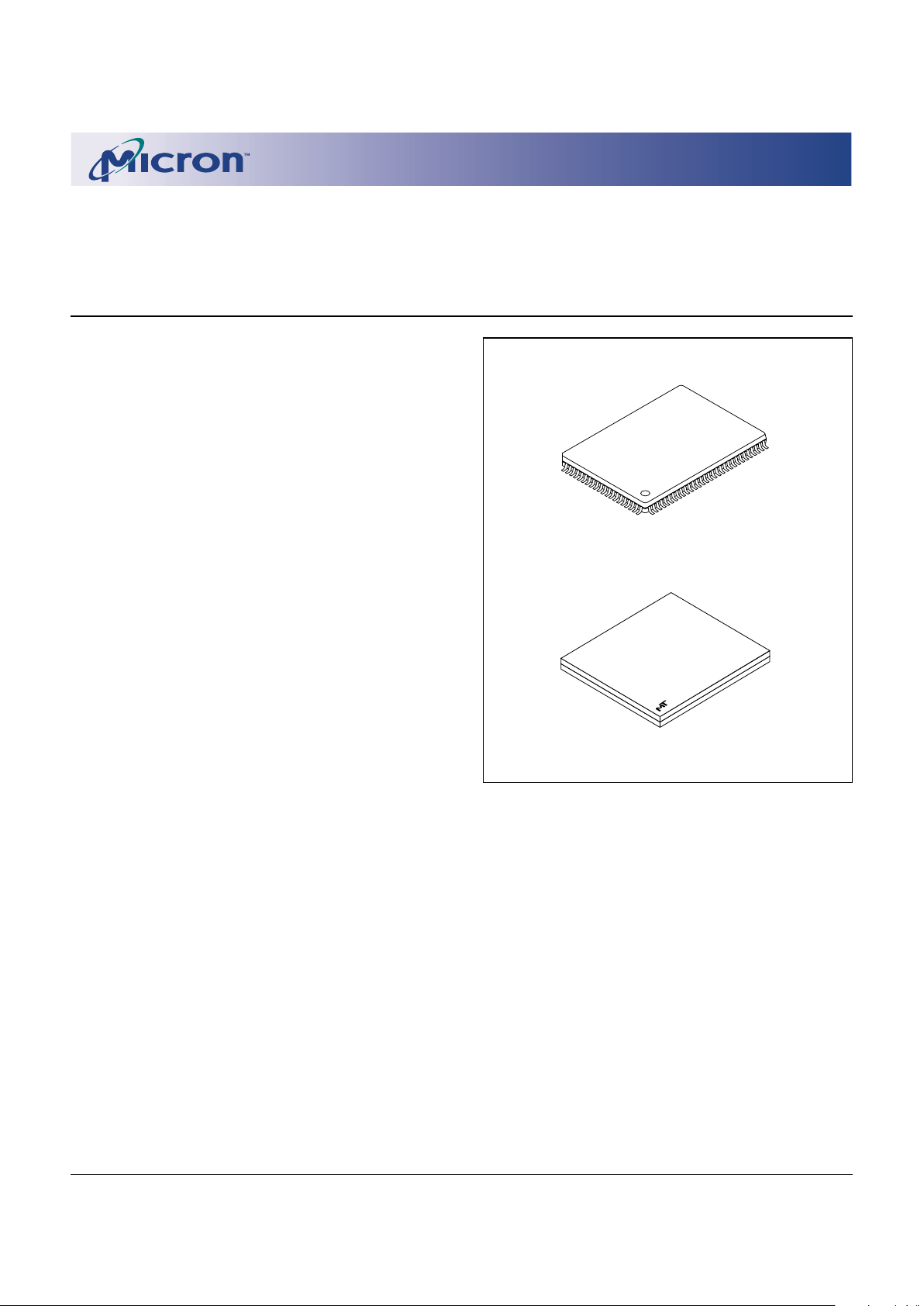
• 100-pin TQFP package
• 165-pin FBGA package
OPTIONS MARKING
• Timing (Access/Cycle/MHz)
3.5ns/6ns/166 MHz -6
4.2ns/7.5ns/133 MHz -7.5
5ns/10ns/100 MHz -10
• Configurations
3.3V I/O
512K x 18 MT55L512L18P
256K x 32 MT55L256L32P
256K x 36 MT55L256L36P
2.5V I/O
512K x 18 MT55L512V18P
256K x 32 MT55L256V32P
256K x 36 MT55L256V36P
• Package
100-pin TQFP T
165-pin, 13mm x 15mm FBGA F*
• Operating Temperature Range
Commercial (0ºC to +70ºC) None
Industrial (-40°C to +85°C)** IT
Part Number Example:
MT55L256L32PT-7.5
MT55L512L18P, MT55L512V18P,
MT55L256L32P, MT55L256V32P,
MT55L256L36P, MT55L256V36P
3.3V VDD, 3.3V or 2.5V I/O
* A Part Marking Guide for the FBGA devices can be found on Micron’s
Web site—http://www.micron.com/support/index.html.
** Industrial temperature range offered in specific speed grades and
configurations. Contact factory for more information.
NOTE: 1. JEDEC-standard MS-026 BHA (LQFP).
100-Pin TQFP
1
165-Pin FBGA
GENERAL DESCRIPTION
The Micron® Zero Bus Turnaround™ (ZBT®) SRAM
family employs high-speed, low-power CMOS designs
using an advanced CMOS process.
Micron’s 8Mb ZBT SRAMs integrate a 512K x 18,
256K x 32, or 256K x 36 SRAM core with advanced
synchronous peripheral circuitry and a 2-bit burst
counter. These SRAMs are optimized for 100 percent
bus utilization, eliminating any turnaround cycles for
READ to WRITE, or WRITE to READ, transitions. All
synchronous inputs pass through registers controlled
by a positive-edge-triggered single clock input (CLK).
The synchronous inputs include all addresses, all data
inputs, chip enable (CE#), two additional chip enables
for easy depth expansion (CE2, CE2#), cycle start input
2
8Mb: 512K x 18, 256K x 32/36 Pipelined ZBT SRAM Micron Technology, Inc., reserves the right to change products or specifications without notice.
MT55L512L18P_C.p65 – Rev. 2/02 ©2002, Micron Technology, Inc.
8Mb: 512K x 18, 256K x 32/36
PIPELINED ZBT SRAM
36 36 36 36 36
K
MODE
18
BWa#
BWb#
BWc#
BWd#
R/W#
CE#
CE2
CE2#
OE#
READ LOGIC
DQs
DQPa
DQPb
DQPc
DQPd
D
A
T
A
S
T
E
E
R
I
N
G
O
U
T
P
U
T
B
U
F
F
E
R
S
256K x 8 x 4
(x32)
256K x 9 x 4
(x36)
MEMORY
ARRAY
E
E
INPUT
REGISTER 0
ADDRESS
REGISTER 0
WRITE ADDRESS
REGISTER 1
WRITE ADDRESS
REGISTER 2
WRITE REGISTRY
AND DATA COHERENCY
CONTROL LOGIC
18
18
16 18
BURST
LOGIC
SA0'
SA1'
D1D0Q1
Q0
SA0
SA1
K
18
ADV/LD#
ADV/LD#
E
INPUT
REGISTER 1
S
E
N
S
E
A
M
P
S
O
U
T
P
U
T
R
E
G
I
S
T
E
R
S
E
CLK
CKE#
WRITE
DRIVERS
SA0, SA1, SA
36
36
36
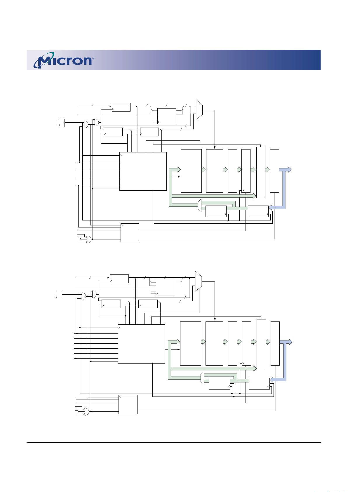
NOTE: Functional block diagrams illustrate simplified device operation. See truth table, pin descriptions, and timing diagrams
for detailed information.
FUNCTIONAL BLOCK DIAGRAM
256K x 32/36
FUNCTIONAL BLOCK DIAGRAM
512K x 18
18 18 18 18
SA0, SA1, SA
K
MODE
19
BWa#
BWb#
R/W#
CE#
CE2
CE2#
OE#
READ LOGIC
DQs
D
A
T
A
S
T
E
E
R
I
N
G
O
U
T
P
U
T
B
U
F
F
E
R
S
512K x 9 x 2
MEMORY
ARRAY
E
E
INPUT
REGISTER 0
ADDRESS
REGISTER 0
WRITE ADDRESS
REGISTER 1
WRITE ADDRESS
REGISTER 2
WRITE REGISTRY
AND DATA COHERENCY
CONTROL LOGIC
19
19
17 19
BURST
LOGIC
SA0'
SA1'
D1D0Q1
Q0
SA0
SA1
K
19
ADV/LD#
ADV/LD#
E
INPUT
REGISTER 1
S
E
N
S
E
A
M
P
S
O
U
T
P
U
T
R
E
G
I
S
T
E
R
S
E
CLK
CKE#
WRITE
DRIVERS
1818
18
18
18

3
8Mb: 512K x 18, 256K x 32/36 Pipelined ZBT SRAM Micron Technology, Inc., reserves the right to change products or specifications without notice.
MT55L512L18P_C.p65 – Rev. 2/02 ©2002, Micron Technology, Inc.
8Mb: 512K x 18, 256K x 32/36
PIPELINED ZBT SRAM
GENERAL DESCRIPTION (continued)
(ADV/LD#), synchronous clock enable (CKE#), byte
write enables (BWa#, BWb#, BWc#, and BWd#), and
read/write (R/W#).
Asynchronous inputs include the output enable
(OE#, which may be tied LOW for control signal minimization), clock (CLK), and snooze enable (ZZ, which
may be tied LOW if unused). There is also a burst mode
pin (MODE) that selects between interleaved and linear
burst modes. MODE may be tied HIGH, LOW, or left
unconnected if burst is unused. The data-out (Q),
enabled by OE#, is registered by the rising edge of CLK.
WRITE cycles can be from one to four bytes wide as
controlled by the write control inputs.
All READ, WRITE, and DESELECT cycles are initiated by the ADV/LD# input. Subsequent burst
addresses can be internally generated as controlled by
the burst advance pin (ADV/LD#). Use of burst mode
is optional. It is allowable to give an address for each
individual READ and WRITE cycle. BURST cycles wrap
around after the fourth access from a base address.
To allow for continuous, 100 percent use of the data
bus, the pipelined ZBT SRAM uses a LATE LATE WRITE
cycle. For example, if a WRITE cycle begins in clock cycle
one, the address is present on rising edge one. BYTE
WRITEs need to be asserted on the same cycle as the
address. The data associated with the address is required
two cycles later, or on the rising edge of clock cycle three.
Address and write control are registered on-chip to
simplify WRITE cycles. This allows self-timed WRITE
cycles. Individual byte enables allow individual bytes to
be written. During a BYTE WRITE cycle, BWa# controls
DQa pins; BWb# controls DQb pins; BWc# controls
DQc pins; and BWd# controls DQd pins. Cycle types
can only be defined when an address is loaded, i.e.,
when ADV/LD# is LOW. Parity/ECC bits are only
available on the x36 version.
Micron’s 8Mb ZBT SRAMs operate from a +3.3V VDD
power supply, and all inputs and outputs are LVTTLcompatible. Users can choose either a 2.5V or 3.3V I/O
version. The device is ideally suited for systems requiring high bandwidth and zero bus turnaround delays.
Please refer to Micron’s Web site (www.micron.com/
sramds) for the latest data sheet.
4
8Mb: 512K x 18, 256K x 32/36 Pipelined ZBT SRAM Micron Technology, Inc., reserves the right to change products or specifications without notice.
MT55L512L18P_C.p65 – Rev. 2/02 ©2002, Micron Technology, Inc.
8Mb: 512K x 18, 256K x 32/36
PIPELINED ZBT SRAM
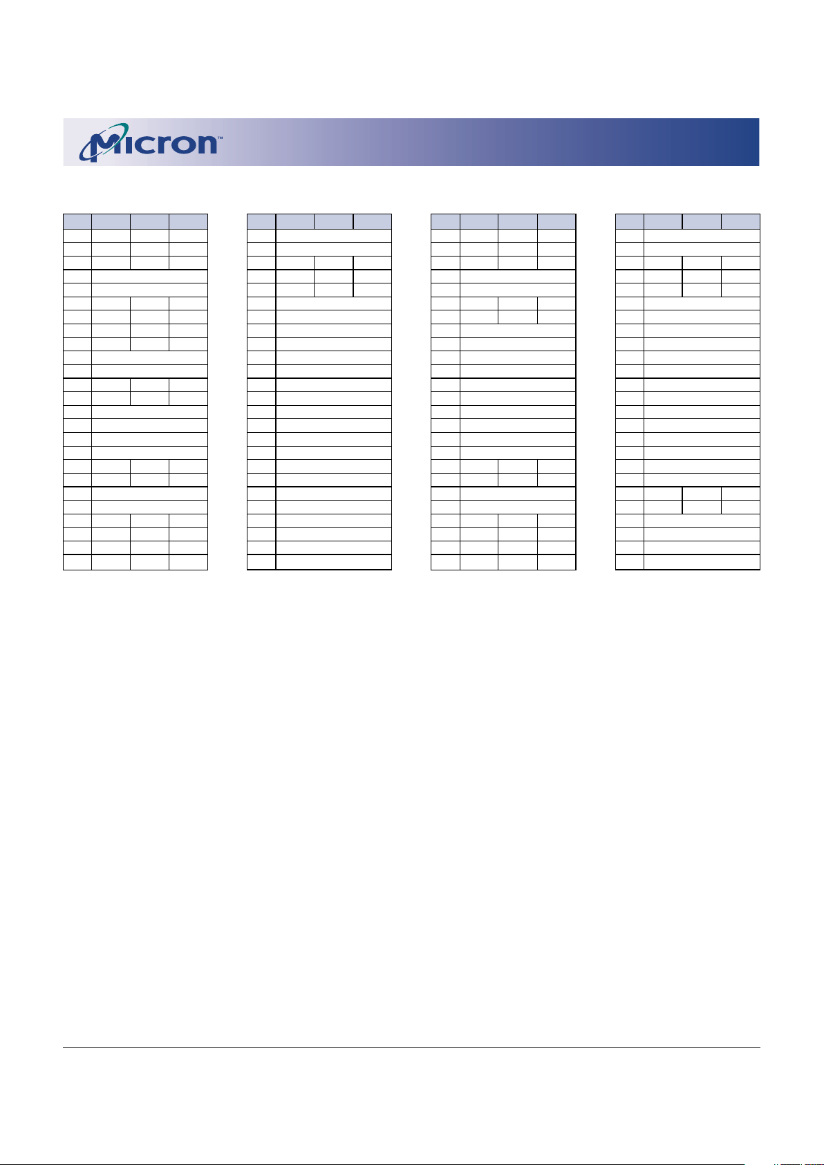
PIN # x18 x32 x36
51 NC NF DQPa
52 NC DQa DQa
53 NC DQa DQa
54 VDDQ
55 VSS
56 NC DQa DQa
57 NC DQa DQa
58 DQa
59 DQa
60 VSS
61 VDDQ
62 DQa
63 DQa
64 ZZ
65 VDD
66 VDD
1
67 VSS
68 DQa DQb DQb
69 DQa DQb DQb
70 VDDQ
71 VSS
72 DQa DQb DQb
73 DQa DQb DQb
74 DQa DQb DQb
75 NC DQb DQb
PIN # x18 x32 x36
76 VSS
77 VDDQ
78 NC DQb DQb
79 NC DQb DQb
80 SA NF DQPb
81 SA
82 SA
83 SA
84 NF
2
85 ADV/LD#
86 OE# (G#)
87 CKE#
88 R/W#
89 CLK
90 VSS
91 VDD
92 CE2#
93 BWa#
94 BWb#
95 NC BWc# BWc#
96 NC BWd# BWd#
97 CE2
98 CE#
99 SA
100 SA
PIN # x18 x32 x36
TQFP PIN ASSIGNMENT TABLE
26 VSS
27 VDDQ
28 NC DQd DQd
29 NC DQd DQd
30 NC NF DQPd
31 MODE (LBO#)
32 SA
33 SA
34 SA
35 SA
36 SA1
37 SA0
38 DNU
39 DNU
40 VSS
41 VDD
42 DNU
43 DNU
44 SA
45 SA
46 SA
47 SA
48 SA
49 SA
50 SA
PIN # x18 x32 x36
1NCNFDQPc
2NCDQc DQc
3NCDQc DQc
4VDDQ
5VSS
6NCDQc DQc
7NCDQc DQc
8 DQb DQc DQc
9 DQb DQc DQc
10 VSS
11 VDDQ
12 DQb DQc DQc
13 DQb DQc DQc
14 VDD
15 VDD
16 VDD
1
17 VSS
18 DQb DQd DQd
19 DQb DQd DQd
20 VDDQ
21 VSS
22 DQb DQd DQd
23 DQb DQd DQd
24 DQb DQd DQd
25 NC DQd DQd
NOTE: 1. Pins 16 and 66 do not have to be connected directly to V
DD if the input voltage is ≥ VIH.
2. Pin 84 is reserved for expansion to 18Mb device.
5
8Mb: 512K x 18, 256K x 32/36 Pipelined ZBT SRAM Micron Technology, Inc., reserves the right to change products or specifications without notice.
MT55L512L18P_C.p65 – Rev. 2/02 ©2002, Micron Technology, Inc.
8Mb: 512K x 18, 256K x 32/36
PIPELINED ZBT SRAM
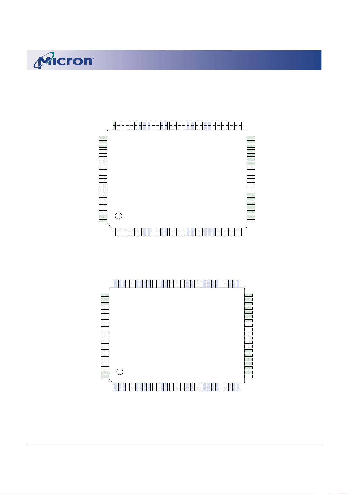
PIN ASSIGNMENT (TOP VIEW)
100-PIN TQFP
SA
SA
SA
NF
2
ADV/LD#
OE# (G#)
CKE#
R/W#
CLK
V
SS
V
DD
CE2#
BWa#
BWb#
NC
NC
CE2
CE#
SA
SA
81
82
83
84
85
86
87
88
89
90
91
92
93
94
95
96
97
98
99
100
50
49
48
47
46
45
44
43
42
41
40
39
38
37
36
35
34
33
32
31
80 79 78 77 76 75 74 73 72 71 70 69 68 67 66 65 64 63 62 61 60 59 58 57 56 55 54 53 52 51
1 2 3 4 5 6 7 8 9 10 11 12 13 14 15 16 17 18 19 20 21 22 23 24 25 26 27 28 29 30
SANCNC
V
DD
Q
V
SS
NC
DQa
DQa
DQa
VSSV
DD
Q
DQa
DQa
V
SSVDD
1
VDDZZ
DQa
DQa
V
DD
Q
V
SS
DQa
DQaNCNC
VSSV
DD
Q
NCNCNC
SA
SA
SA
SA
SA
SA
SA
DNU
DNU
V
DD
V
SS
DNU
DNU
SA0
SA1
SA
SA
SA
SA
MODE
(LBO#)
NCNCNC
V
DD
Q
V
SS
NC
NC
DQb
DQb
V
SS
V
DD
Q
DQb
DQb
V
DDVDD
V
DD
1
V
SS
DQb
DQb
V
DD
Q
V
SS
DQb
DQb
DQb
NC
V
SS
V
DD
Q
NCNCNC
x18
SA
SA
SA
NF
2
ADV/LD#
OE# (G#)
CKE#
R/W#
CLK
V
SS
V
DD
CE2#
BWa#
BWb#
BWc#
BWd#
CE2
CE#
SA
SA
81
82
83
84
85
86
87
88
89
90
91
92
93
94
95
96
97
98
99
100
50
49
48
47
46
45
44
43
42
41
40
39
38
37
36
35
34
33
32
31
80 79 78 77 76 75 74 73 72 71 70 69 68 67 66 65 64 63 62 61 60 59 58 57 56 55 54 53 52 51
1 2 3 4 5 6 7 8 9 10 11 12 13 14 15 16 17 18 19 20 21 22 23 24 25 26 27 28 29 30
NF/DQPb3DQb
DQb
V
DD
Q
V
SS
DQb
DQb
DQb
DQb
VSSV
DD
Q
DQb
DQb
V
SSVDD
1
VDDZZ
DQa
DQa
V
DD
Q
V
SS
DQa
DQa
DQa
DQa
VSSV
DD
Q
DQa
DQa
NF/DQPa
3
SA
SA
SA
SA
SA
SA
SA
DNU
DNU
V
DD
V
SS
DNU
DNU
SA0
SA1
SA
SA
SA
SA
MODE
(LBO#)
NF/DQPc
3
DQc
DQc
V
DD
Q
V
SS
DQc
DQc
DQc
DQc
V
SS
V
DD
Q
DQc
DQc
V
DDVDD
V
DD
1
V
SS
DQd
DQd
V
DD
Q
V
SS
DQd
DQd
DQd
DQd
V
SS
V
DD
Q
DQd
DQd
NF/DQPd
3
x32/x36
NOTE: 1. Pins 16 and 66 do not have to be connected directly to VDD if the input voltage is ≥ VIH.
2. Pin 84 is reserved for expansion to 18Mb device.
3. NF for x32 version, DQPx for x36 version.
6
8Mb: 512K x 18, 256K x 32/36 Pipelined ZBT SRAM Micron Technology, Inc., reserves the right to change products or specifications without notice.
MT55L512L18P_C.p65 – Rev. 2/02 ©2002, Micron Technology, Inc.
8Mb: 512K x 18, 256K x 32/36
PIPELINED ZBT SRAM
TQFP PIN DESCRIPTIONS
x18 x32/x36 SYMBOL TYPE DESCRIPTION
37 37 SA0 Input Synchronous Address Inputs: These inputs are registered
36 36 SA1 and must meet the setup and hold times around the rising
32-35, 44-50, 32-35, 44-50, SA edge of CLK. Pin 84 is reserved as an address bit for
80-83, 99, 100 81-83, 99, 100 higher-density 18Mb ZBT SRAMs. SA0 and SA1 are the
two least significant bits (LSB) of the address field and
set the internal burst counter if burst is desired.
93 93 BWa# Input Synchronous Byte Write Enables: These active LOW inputs
94 94 BWb# allow individual bytes to be written when a WRITE cycle is
– 95 BWc# active and must meet the setup and hold times around the
– 96 BWd# rising edge of CLK. BYTE WRITEs need to be asserted on
the same cycle as the address. BWs are associated with
addresses and apply to subsequent data. BWa# controls
DQa pins; BWb# controls DQb pins; BWc# controls DQc
pins; BWd# controls DQd pins.
89 89 CLK Input Clock: This signal registers the address, data, chip enables,
byte write enables, and burst control inputs on its rising
edge. All synchronous inputs must meet setup and hold
times around the clock’s rising edge.
98 98 CE# Input Synchronous Chip Enable: This active LOW input is used to
enable the device and is sampled only when a new
external address is loaded (ADV/LD# is LOW).
92 92 CE2# Input Synchronous Chip Enable: This active LOW input is used to
enable the device and is sampled only when a new
external address is loaded (ADV/LD# is LOW). This
input can be used for memory depth expansion.
97 97 CE2 Input Synchronous Chip Enable: This active HIGH input is used to
enable the device and is sampled only when a new
external address is loaded (ADV/LD# is LOW). This
input can be used for memory depth expansion.
86 86 OE# Input Output Enable: This active LOW, asynchronous input
(G#) enables the data I/O output drivers. G# is the JEDEC-
standard term for OE#.
85 85 ADV/LD# Input Synchronous Address Advance/Load: When HIGH, this
input is used to advance the internal burst counter,
controlling burst access after the external address is
loaded. When ADV/LD# is HIGH, R/W# is ignored. A LOW
on ADV/LD# clocks a new address at the CLK rising edge.
87 87 CKE# Input Synchronous Clock Enable: This active LOW input permits
CLK to propagate throughout the device. When CKE# is
HIGH, the device ignores the CLK input and effectively
internally extends the previous CLK cycle. This input must
meet setup and hold times around the rising edge of CLK.
64 64 ZZ Input Snooze Enable: This active HIGH, asynchronous input
causes the device to enter a low-power standby mode in
which all data in the memory array is retained. When ZZ is
active, all other inputs are ignored.
(continued on next page)

7
8Mb: 512K x 18, 256K x 32/36 Pipelined ZBT SRAM Micron Technology, Inc., reserves the right to change products or specifications without notice.
MT55L512L18P_C.p65 – Rev. 2/02 ©2002, Micron Technology, Inc.
8Mb: 512K x 18, 256K x 32/36
PIPELINED ZBT SRAM
TQFP PIN DESCRIPTIONS (CONTINUED)
x18 x32/x36 SYMBOL TYPE DESCRIPTION
88 88 R/W# Input Read/Write: This input determines the cycle type when
ADV/LD# is LOW and is the only means for determining
READs and WRITEs. READ cycles may not be converted into
WRITEs (and vice versa) other than by loading a new
address. A LOW on this pin permits BYTE WRITE operations
and must meet the setup and hold times around the rising
edge of CLK. Full bus-width WRITEs occur if all byte write
enables are LOW.
31 31 MODE Input Mode: This input selects the burst sequence. A LOW on
(LBO#) this pin selects linear burst. NC or HIGH on this pin selects
interleaved burst. Do not alter input state while device is
operating. LBO# is the JEDEC-standard term for MODE.
(a) 58, 59, 62, 63, (a) 52, 53, 56-59, DQa Input/ SRAM Data I/Os: Byte “a” is associated with DQa pins;
68, 69, 72-74 62, 63 Output Byte “b” is associated with DQb pins; Byte “c” is
(b) 8, 9, 12, 13, (b) 68, 69, 72-75, DQb associated with DQc pins; Byte “d” is associated with
18, 19, 22-24 78, 79 DQd pins. Input data must meet setup and hold times
(c) 2, 3, 6-9, DQc around the rising edge of CLK.
12, 13
(d) 18, 19, 22-25, DQd
28, 29
n/a 51 NF/DQPa NF/ No Function/Data Bits: On the x32 version, these pins are
80 NF/DQPb I/O No Function (NF) and can be left floating or connected to
1 NF/DQPc GND to minimize thermal impedance. On the x36 version,
30 NF/DQPd these bits are DQPs.
14, 15, 16, 41, 65, 14, 15, 16, 41, 65, V
DD
Supply Power Supply: See DC Electrical Characteristics and
66, 91 66, 91 Operating Conditions for range.
4, 11, 20, 27, 4, 11, 20, 27, VDDQ Supply Isolated Output Buffer Supply: See DC Electrical
54, 61, 70, 77 54, 61, 70, 77 Characteristics and Operating Conditions for range.
5, 10, 17, 21, 5, 10, 17, 21, V
SS
Supply Ground: GND.
26, 40, 55, 60, 26, 40, 55, 60,
67, 71, 76, 90 67, 71, 76, 90
1-3, 6, 7, 25, n/a NC – No Connect: These pins can be left floating or connected
28-30, 51-53, 56, to GND to minimize thermal impedance.
57, 75, 78, 79,
95, 96
38, 39, 42, 43 38, 39, 42, 43 DNU – Do Not Use: These signals may either be unconnected or
wired to GND to minimize thermal impedance.
84 84 NF – No Function: This pin is internally connected to the die and
will have the capacitance of an input pin. It is allowable to
leave this pin unconnected or driven by signals. Pin 84 is
reserved as an address pin for the 18Mb ZBT SRAM.
8
8Mb: 512K x 18, 256K x 32/36 Pipelined ZBT SRAM Micron Technology, Inc., reserves the right to change products or specifications without notice.
MT55L512L18P_C.p65 – Rev. 2/02 ©2002, Micron Technology, Inc.
8Mb: 512K x 18, 256K x 32/36
PIPELINED ZBT SRAM
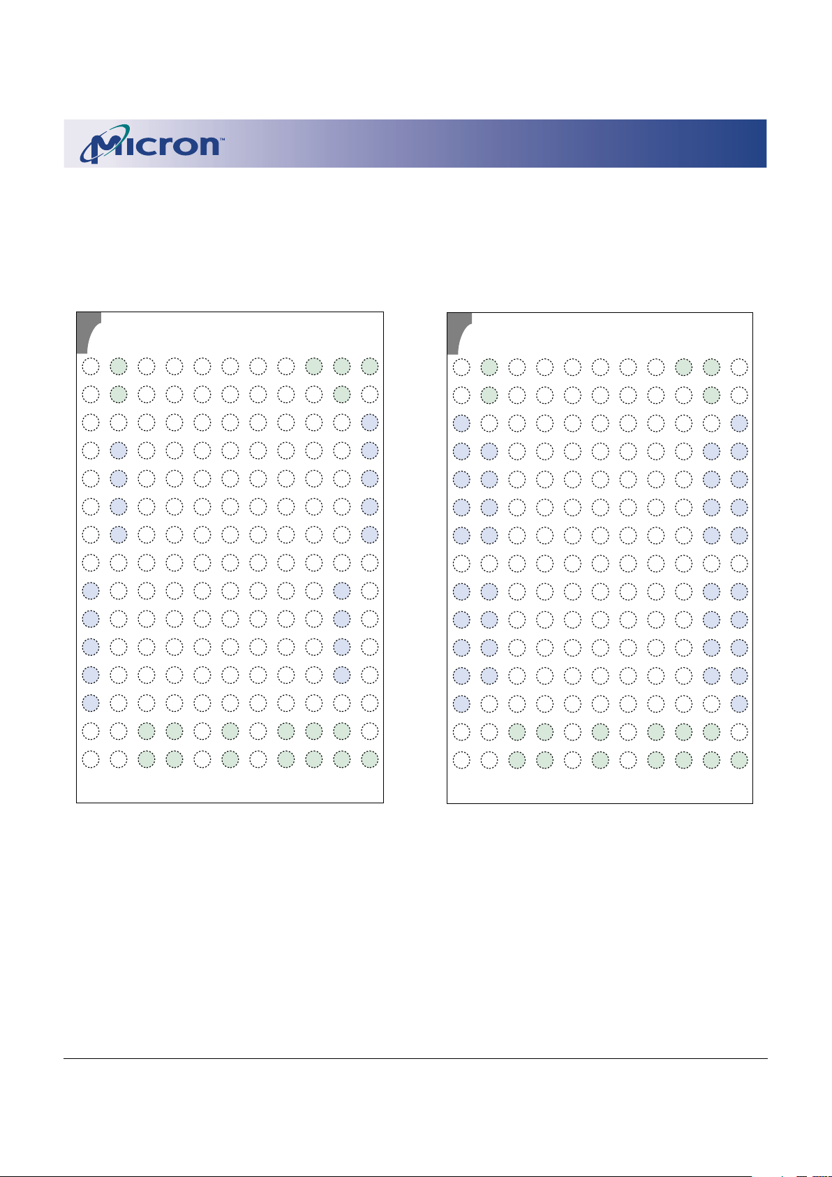
PIN LAYOUT (TOP VIEW)
165-PIN FBGA
A
B
C
D
E
F
G
H
J
K
L
M
N
P
R
A
B
C
D
E
F
G
H
J
K
L
M
N
P
R
2
CE#
CE2
V
DD
Q
V
DD
Q
V
DD
Q
V
DD
Q
V
DD
Q
NC
V
DD
Q
V
DD
Q
V
DD
Q
V
DD
Q
V
DD
Q
SA
SA
SA
SA
NC
DQb
DQb
DQb
DQb
V
DD
NC
NC
NC
NC
NC
NC
NC
NC
NC
NC
NC
NC
NC
NC
V
DD
DQb
DQb
DQb
DQb
NF/DQPb
NC
MODE
(LBO#)
BWb#
NC
V
SS
V
DD
V
DD
V
DD
V
DD
V
DD
V
DD
V
DD
V
DD
V
DD
V
SS
SA
SA
NC
BWa#
V
SS
V
SS
V
SS
V
SS
V
SS
V
SS
V
SS
V
SS
V
SS
V
SS
NC
DNU
DNU
CE2#
CLK
V
SS
V
SS
V
SS
V
SS
V
SS
V
SS
V
SS
V
SS
V
SS
V
SS
NC
SA1
SA0
CKE#
R/W#
V
SS
V
SS
V
SS
V
SS
V
SS
V
SS
V
SS
V
SS
V
SS
V
SS
V
DD
DNU
DNU
ADV/L D#
OE# (G#)
V
SS
V
DD
V
DD
V
DD
V
DD
V
DD
V
DD
V
DD
V
DD
V
DD
V
SS
SA
SA
SA
NC
V
DD
Q
V
DD
Q
V
DD
Q
V
DD
Q
V
DD
Q
NC
V
DD
Q
V
DD
Q
V
DD
Q
V
DD
Q
V
DD
Q
SA
SA
SA
SA
NC
NC
NC
NC
NC
NC
DQa
DQa
DQa
DQa
NC
SA
SA
SA
NC
NF/DQPa
DQa
DQa
DQa
DQa
ZZ
NC
NC
NC
NC
NC
NC
SA
TOP VIEW
3456789
10 11
1
A
B
C
D
E
F
G
H
J
K
L
M
N
P
R
A
B
C
D
E
F
G
H
J
K
L
M
N
P
R
2
CE#
CE2
V
DD
Q
V
DD
Q
V
DD
Q
V
DD
Q
V
DD
Q
NC
V
DD
Q
V
DD
Q
V
DD
Q
V
DD
Q
V
DD
Q
SA
SA
SA
SA
NC
DQc
DQc
DQc
DQc
V
DD
DQd
DQd
DQd
DQd
NC
NC
NC
NC
NC
NF/DQPc
DQc
DQc
DQc
DQc
V
DD
DQd
DQd
DQd
DQd
NF/DQPd
NC
MODE
(LBO#)
BWc#
BWd#
V
SS
V
DD
V
DD
V
DD
V
DD
V
DD
V
DD
V
DD
V
DD
V
DD
V
SS
SA
SA
BWb#
BWa#
V
SS
V
SS
V
SS
V
SS
V
SS
V
SS
V
SS
V
SS
V
SS
V
SS
NC
DNU
DNU
CE2#
CLK
V
SS
V
SS
V
SS
V
SS
V
SS
V
SS
V
SS
V
SS
V
SS
V
SS
NC
SA1
SA0
CKE#
R/W#
V
SS
V
SS
V
SS
V
SS
V
SS
V
SS
V
SS
V
SS
V
SS
V
SS
V
DD
DNU
DNU
ADV/LD#
OE# (G#)
V
SS
V
DD
V
DD
V
DD
V
DD
V
DD
V
DD
V
DD
V
DD
V
DD
V
SS
SA
SA
SA
NC
V
DD
Q
V
DD
Q
V
DD
Q
V
DD
Q
V
DD
Q
NC
V
DD
Q
V
DD
Q
V
DD
Q
V
DD
Q
V
DD
Q
SA
SA
SA
SA
NC
DQb
DQb
DQb
DQb
NC
DQa
DQa
DQa
DQa
NC
SA
SA
NC
NC
NF/DQPb
DQb
DQb
DQb
DQb
ZZ
DQa
DQa
DQa
DQa
NF/DQPa
NC
SA
TOP VIEW
3456789
10 11
1
X18
X32/X36
*No Function (NF) is used on the x32 version. Parity (DQPx) is used on the x36 version.
NOTE: Pin 9B reserved for address pin expansion; 18Mb.
 Loading...